Philips LX9000R Service Manual
Dvd+rw receiver
Hide thumbs
Also See for LX9000R:
- Manual (77 pages) ,
- Quick use manual (6 pages) ,
- Specification sheet (2 pages)
Table of Contents
Advertisement
DVD+RW Receiver
For servicing the DVD+RW Basic Engine we refer to
Service Manual 3122 785 12473
DVD+RW Basic Engine VAE8015, VAE8020
Only designated workshops can perform these repairs!
TABLE OF CONTENTS
Technical specification..........................................................2
Locartion of printed circuit boards.........................................4
Warnings & Safety ................................................................5
Brief Operating Instructions ..................................................6
Dismantling Instructions......................................................15
Service hints .......................................................................24
Diagnostic Software............................................................25
Block Diagrams...................................................................59
Exploded Views ..................................................................64
Control board ......................................................................65
Key board left......................................................................67
Key board left 2...................................................................68
A/V Front connectors ..........................................................68
Key board right ...................................................................69
Power Supply primary.........................................................71
Power Supply secondary ....................................................72
Auxiliary board ....................................................................75
©
Copyright 2003 Philips Consumer Electronics B.V. Eindhoven, The Netherlands
All rights reserved. No part of this publication may be reproduced, stored in a retrieval
system or transmitted, in any form or by any means, electronic, mechanical, photocopying,
or otherwise without the prior permission of Philips.
Published by MS 0329 Service Audio
Version 1.0
Printed in The Netherlands
Subject to modification
ASP (Audio Signal Processing) board ................................77
MDM (Multi-channel Decvoding Module) board .................82
Amplifier board....................................................................85
Loudspeaker Socket board.................................................90
A/V board............................................................................91
µP Sub board (CECO) ........................................................99
DVIO board.......................................................................103
Digital board......................................................................112
Alignments ........................................................................129
Circuit- and IC descriptions...............................................132
Abbreviations A/V-, Digital-, DVIO board..........................211
Abbreviations set related ..................................................217
Spare parts list..................................................................220
LX9000R
/22/25/29
CLASS 1
©
3103 785 25200
Advertisement
Table of Contents

Related Manuals for Philips LX9000R


Summary of Contents for Philips LX9000R
-
Page 1: Table Of Contents
LASER PRODUCT © Copyright 2003 Philips Consumer Electronics B.V. Eindhoven, The Netherlands All rights reserved. No part of this publication may be reproduced, stored in a retrieval system or transmitted, in any form or by any means, electronic, mechanical, photocopying, or otherwise without the prior permission of Philips. -
Page 2: Technical Specification
Frequency response at SCART 1 (L+R) output :100 Hz - 12 kHz / 0± 3dB Pin Signals: S/N according to DIN 45405, 7, 1967 and PHILIPS standard test Audio R 1.8V RMS pattern video signal :FM: ≥ 50dB Audio R AM ≥... - Page 3 Technical specification LX9000R EN 3 Video - YC (Hosiden) Power Amplifier Input voltage Y :1Vpp ± 3dB Power stage protection :temperature and short circuit Input impedance Y :75 W Output power Input voltage C :burst 300 mVpp ± 3 dB...
- Page 4 EN 4 LX9000R Location of printed boards LOCATION OF PRINTED BOARDS Location PCBs LX9000R, 100703 figure 1...
-
Page 5: Safety Information
Safety Information LX9000R EN 5 © ñ WARNING WAARSCHUWING All ICs and many other semiconductors are susceptible to Alle IC´s en vele andere halfgeleiders zijn gevoelig voor electrostatic discharges (ESD). Careless handling during electrostatische ontladingen (ESD). repair can reduce life drastically. -
Page 6: Brief Operating Instructions
The following excerpt of the Owner´s Manual serves as a very short introduction to the set. The complete Owners Manual can be downloaded in several languages from the Internet site of Philips Customer Care Center: www.p4c.philips.com Controls and connections 3456 &... -
Page 7: Controls And Connections
Brief Operating Instructions LX9000R EN 7 Controls and connections FRONT LEFT 4 Ω RADIO MAINS FRONT RIGHT 4 Ω TV ANTENNA EXT 2 CENT. 4 Ω LINE IN 1 LINE IN 2 LINE OUT DIGITAL OUT AUX I/0 LEFT 8 Ω... -
Page 8: Remote Control
É É Using the remote control With this remote control you can control the DVD recorder system as well as other Philips appliances such as a Philips TV,VCR or CD player. MUTE To control a Philips appliance, briefly press the... -
Page 9: Remote Control Keys
EN 9 Remote Control Remote control keys / – TV VOL switches the DVD recorder system and a Philips appliance skips to the beginning of the current or previous on or to standby chapter/title/track of the inserted disc, searches backwards,... -
Page 10: General Information
EN 10 LX9000R Brief Operating Instructions Quick use guide LX9000R General information Supplied accessories 1 2 batteries for the remote control, type AA This Quick use guide gives a rough overview and helps to quickly start with basic steps. Please read the supplied 2 1 remote control user´s manual for detailed information. -
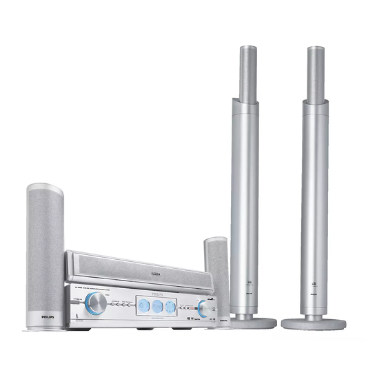
Page 11: Positioning The Speakers
Brief Operating Instructions LX9000R EN 11 Quick use guide LX9000R Assembling the speakers Subwoofers and front speakers Rear speakers to place the rear speakers on a shelf or on the floor to hang the rear speakers on the wall Positioning the speakers Connecting the speakers Connect the speakers using the supplied speaker cables. -
Page 12: Initial Installation
EN 12 LX9000R Brief Operating Instructions Quick use guide LX9000R FM ANTENNA ANTENNA IN EXT IN AM ANTENNA RADIO MAINS TV ANTENNA EXT 2 LINE IN 1 LINE IN 2 LINE OUT DIGITAL OUT AUX I/0 EXT 1 TV OUT... - Page 13 Brief Operating Instructions LX9000R EN 13 Quick use guide LX9000R The menu Subtitle Language appears. Press OK. CONTINUE WITH SPECIAL AUDIO SETTINGS is Press 3 or 4 to select the language in which subtitles scrolled on the DVD recorder system.
-
Page 14: Selecting A Source
EN 14 LX9000R Brief Operating Instructions Quick use guide LX9000R Discs for playback and recording Playback Press OPEN/CLOSE / on the set to open the drawer and – DVD+R can be recorded once and played insert a disc (printed side up) in the tray. -
Page 15: Dismantling Instructions
Dismantling Instructions LX9000R EN 15 DISMANTLING INSTRUCTIONS Dismantling the Top Cover Manual opening of the tray • Remove 9 screws as shown in picture 1. In case the loader is defect or cannot be opened electrically, proceed • Raise top cover at the rear and pull it backwards. - Page 16 EN 16 LX9000R Dismantling Instructions Removal of Air guide plate Dismantling the MDM Board • Remove 5 screws as shown in picture 6. • Release catches as shown in picture 8. • Remove cables from the guidings • Lift MDM Board on the outer side and move it left to •...
- Page 17 Dismantling Instructions LX9000R EN 17 Dismantling the ASP Board Dismantling the Amplifier Board • Dismantle MDM Board (as described before) first. • Dismantle MDM Board and ASP Board (as described before) first. • Release catches as shown in picture 8.
- Page 18 EN 18 LX9000R Dismantling Instructions Dismantling the Power secondary Board • Dismantle MDM- and ASP Board (as described before) first. • Unplug headphone cable from ASP Board and put it out from the catches on the Power secondary support frame.
- Page 19 Dismantling Instructions LX9000R EN 19 Dismantling the Front panel assembly The front panel assy consists of 2 cabinet parts, the ornamental aluminium front and the plastic front cabinet where the printed circuit boards and other technical parts are mounted. Dependent on the location which is wanted to be accessed the front panel assy can be detached either as complete assy or separated in aluminium front and plastic front.
- Page 20 EN 20 LX9000R Dismantling Instructions Dismantling the Plastic Front cabinet • Loosen 8 screws as shown in picture 23 and 24. • Plug Firewire cable from DVIO Board off 1 and release all cables as shown in picture 29 to give them a proper free length for moving front assy out.
- Page 21 Dismantling Instructions LX9000R EN 21 Dismantling Knobs of the Rotary Encoders Dismantling the Display • Dismantle ornamental Aluminium Front as described before. • Dismantle ornamental Aluminium Front as described before. • Turn the knob to a position as shown in picture 35.
- Page 22 EN 22 LX9000R Dismantling Instructions Dismantling the DVD Basic Engine Dismantling the Digital Board • Dismantle Top Cover and Air guide plate as described before. • Dismantle Top Cover and Air guide plate as described before. • Loosen 4 screws as shown in picture 40.
- Page 23 Dismantling Instructions LX9000R EN 23 picture 45 picture 46 picture 47 Analog Board picture 48...
-
Page 24: Service Hints
EN 24 LX9000R Service hints SERVICE TOOLS TORX T10 screwdriver with shaftlength 150mm..4822 395 50423 Sub chassis 8 test disc CD........7104 099 28362 TORX screwdriver set SBC 163......4822 295 50145 MPTD printed test disc CVP02.18A.......7104 099 91691 MPTD printed test disc CVP02.18C ......7104 099 97941 Audio signal disc SBC 429 ........4822 397 30184... -
Page 25: Diagnostic Software
To toggle Video Mode To toggle Modulator Channel Virgin Mode (interlace/progressive scan) (channel 3/4) hold hold STANDBY button hold STOP button depressed RECORD button depressed depressed while plugging mainscord in. while plugging mainscord in. while plugging mainscord in. servtest LX9000R sh 1, 210703... - Page 26 PLAY button STOP button S or T button pressed? pressed? pressed? Switch speed of set fan to next/previous step. Back to main menu. Display shows FAN SPD X for 2s. x= 1, 2, 3, 4 servtest LX9000R sh 2, 040503...
- Page 27 Switch intensity of the Switch on LEDs in following Back to main menu. backlight diodes to next step. sequence: (toggles backlight intensity Standby, Instant Record, to half / off / full intensity) Record, off servtest LX9000R sh 3, 060503...
- Page 28 The correct tuner version is defined by the version detection resistor 3444 mounted on Service Testprogram. the Front - Control board. 3444 mounted = USA version without RDS. The stored preset frequencies serve as provision for other tuner modules only. servtest LX9000R sh 4, 100503...
- Page 29 Optical Input. EEPROM SRAM error error error e.g. 001 means DSP error Display shows 101 means DSP plus EEPROM error MDM error? OPT ER Display shows PLAY button pressed? Back to main menu. servtest LX9000R sh 5, 140603...
- Page 30 (Headhone and Line out Loudspeakers) AMP 1 Line in 1 AMP 2 Line in 2 AMP 3 Ext. 1 AMP 4 Ext. 2 AMP 5 Line in 1 AMP 6 Line in 2 table 4 servtest LX9000R sh 6, 100503...
- Page 31 Diagnostic Software DVD LX9000R EN 31 5. Diagnostic Software DVD Due to the complexity of the DVD recorder, the time to find a 5.1.2 Contents defect in the recorder can become long. To reduce this time, the recorder has been equipped with Diagnostic and Service software (DS).
- Page 32 EN 32 LX9000R Diagnostic Software DVD Counter Nucleus Name Description LoopAudioUserDealer This nucleus tests the components on the audio signal path The host decoder - The analogue board - The audio encoder - The VSM Attention: the rear cinch audio out has to be connected to the front cinch audio in.
- Page 33 (script) To start the DVD Player test hold Open/Close & PLAY buttons depressed while plugging mainscord in. Press 7x STOP to skip general set tests not applicable for LX9000R DIGITAL BOARD & A/V BOARD TEST BASIC ENGINE TEST Figure 5-2...
- Page 34 EN 34 LX9000R Diagnostic Software DVD DIGITAL BOARD & FRONTPANEL ANALOG BOARD BASIC ENGINE TEST TEST TEST press <PLAY> to execute press <PLAY> to execute press < STOP > to skip press <NEXT > to skip press <PLAY> to execute press <...
- Page 35 Diagnostic Software DVD LX9000R EN 35 5.2.3 Error Log Group number Group name Analogue board (DVDR only) Explanation: DVIO (DVDR only) The application errors will be logged in the NVRAM. The Loop nuclei (DVDR only) maximum number of error bytes that will be visible is 19. The...
- Page 36 EN 36 LX9000R Diagnostic Software DVD Command Overview [xx yy] Nuclei We provide an overview of the nuclei and their numbers. This Number overview is preliminary and subject to modifications. Audio Encoder I2C SAA7118 select input Host Decoder [01] Empress Version...
- Page 37 Diagnostic Software DVD LX9000R EN 37 [xx yy] Nuclei [xx yy] Nuclei Number Number Radial Off Store external presets Tray In Get slash version Tray Out AFC Reference Voltage Tuner Write Read Get EPG Version Write Read Endless Loop Get operating hours in Tuner Mode...
- Page 38 EN 38 LX9000R Diagnostic Software DVD The paths that are available for video routing and their description (Nafta region): Example PATH ID DESCRIPTION DD:> 712 01 Input signal is from FRONT AUDIO IN and will 71200: Video routing on the Analogue Board OK.
- Page 39 Diagnostic Software DVD LX9000R EN 39 Menu Structure AVENC Menu The following menu structure is given after starting up the DVD 1.Empress -> recorder in menu mode. The symbol -> indicates that the 2.Video Input Processors -> current menu choice will invoke the display of a submenu.
- Page 40 EN 40 LX9000R Diagnostic Software DVD 2.S2B Pass-through 3.User/Dealer Video Loop VBI 3.S2B Echo 4.Focus On System Loops Menu 5.Focus Off 1.System Video Loop 6.Version 2.System Video Loop VBI 7.Self Test 3.System Audio Loop SCART(EURO) 8.Get Self Test Result 4.System Audio Loop CINCH (NAFTA) 9.Basic Engine Test...
- Page 41 Diagnostic Software DVD LX9000R EN 41 Error Nr Error String Error Nr Error String 10901 "Error muting audio" 20202 "SAA7118 VIP access time-out" 11000 "" 20203 "No acknowledge from SAA7118 VIP" 11001 "Error demuting audio" 20204 "No data received from SAA7118 VIP"...
- Page 42 EN 42 LX9000R Diagnostic Software DVD Error Nr Error String Error Nr Error String 20700 "" 30205 " VSM SDRAM Bank2 Memory addressbus test goes wrong." 20701 "Error audio encoder I2C cannot reset DSP through I2C" 30206 " VSM SDRAM Bank2 Physical memory device test goes wrong."...
- Page 43 Diagnostic Software DVD LX9000R EN 43 Error Nr Error String Error Nr Error String 50204 "Execution of the command on the analogue board 50904 "The user skipped the FP-horizontal segments failed." test." 50205 "The frontpanel could not be accessed by the ana- 50905 "The user returned an unknown confirmation: con-...
- Page 44 EN 44 LX9000R Diagnostic Software DVD Error Nr Error String Error Nr Error String 52005 "The user returned an unknown confirmation: con- 60902 "Parity error from Basic Engine to Serial" firmation" 60903 "Communication time-out error" 52200 "" 60904 "Unexpected response from Basic Engine"...
- Page 45 Diagnostic Software DVD LX9000R EN 45 Error Nr Error String Error Nr Error String 62101 "Basic Engine returned error number 63103 "Communication time-out error" 0xerrornumber" 63104 "Unexpected response from Basic Engine" 62102 "Parity error from Basic Engine to Serial" 63200 ""...
- Page 46 EN 46 LX9000R Diagnostic Software DVD Error Nr Error String Error Nr Error String 64118 "The VSM Sector processor initialisation failed" 71201 "Routing the video on the Analogue Board fails." 64119 "The VSM sector processor DMA initialisation 71202 "Invalid input."...
- Page 47 Diagnostic Software DVD LX9000R EN 47 Error Nr Error String Error Nr Error String 73203 "Communication with Analogue Board fails" 80316 "VSM UART frame error occurred receiving from DVIO board" 80000 "The DVIO module is present in the system." 80317 "VSM UART parity error occurred receiving from...
- Page 48 EN 48 LX9000R Diagnostic Software DVD Error Nr Error String Error Nr Error String 80517 "VSM UART parity error occurred receiving from 80713 "We tried to receive an Acknowledge for DVIO board" DVIO_MAX_RETRIES_ACK times!" 80518 "The confirmation/indication from the DVIO module 80714 "VSM UART error timeout transmitting command"...
- Page 49 Diagnostic Software DVD LX9000R EN 49 Error Nr Error String Error Nr Error String 90229 "The video encoder did not switch from IDLE to 90507 "No CC data received" STOP mode." 90508 "Closed Caption data overrun" 90300 "" 90509 "Closed Caption data does not match"...
- Page 50 EN 50 LX9000R Diagnostic Software DVD Error Nr Error String Error Nr Error String 90801 "Error routing the audio back to the digital board." 90925 "The audio frame has an illegal bitrate-index" 90802 "Error cannot initialise I2C" 90926 "The audio frame has an illegal sampling rate"...
- Page 51 Diagnostic Software DVD LX9000R EN 51 DVIO 1.8 Error Codes Error Code Description Hardware 0x00 DVIOC_ERR_DDS_OK No Error 0x06 DVIOC_ERR_DDS_UNKNOWN Unknown Error(including UART communication error) 0x11 DVIOC_ERR_DDS_TNF_1 Link chip incorrect responding µPD72893, Link 0x12 DVIOC_ERR_DDS_TNF_2 No link register access or link reset failed µPD72893, Link...
- Page 52 EN 52 LX9000R Diagnostic Software DVD 5.5.1 Nucleus 900: Digital Audio Loop 5.5.2 Nucleus 901: Audio User Dealer Loop This nucleus tests the audio path through the digital board This Nucleus is only possible in NAFTA sets. A PCM audio sine of 12kHz is generated in the Host Decoder for a while and sent to the analogue board.
- Page 53 Diagnostic Software DVD LX9000R EN 53 5.5.4 Nucleus 903: Digital Video VBI Loop Nucleus for testing the components on the video VBI signal NUCLEUS 902: DIGITAL VIDEO LOOP path: • The VIP • The VSM • The Host Decoder This is done by using the internal test signal source (digital...
- Page 54 EN 54 LX9000R Diagnostic Software DVD 5.5.5 Nucleus 904: System Video Loop 5.5.6 Nucleus 905: System Video VBI Loop Nucleus for testing the components on the video signal system This nucleus tests the components on the video signal path: path: •...
- Page 55 Diagnostic Software DVD LX9000R EN 55 5.5.7 Nucleus 906: Video User Dealer Loop 5.5.8 Nucleus 907: Video VBI User Dealer Loop Nucleus for testing the components on the video signal system This nucleus tests the components on the video VBI signal...
- Page 56 EN 56 LX9000R Diagnostic Software DVD 5.5.9 Nucleus 908: System Audio Loop Scart (Europe) 5.5.10 Nucleus 909: System Audio Loop CINCH (Nafta) Nucleus for testing the components on the audio signal path: Nucleus for testing the components on the audio signal path: •...
- Page 57 Diagnostic Software DVD LX9000R EN 57 ing to the parameter. There it will be looped back externally by means of the proper cable. The correct Routing path has to be selected by a parameter: Analog board Selectable Internal call to...
- Page 58 EN 58 LX9000R Diagnostic Software DVD...
- Page 59 2, 1208 Power sec. board 1986 IPFAIL 13P PH/SAN 170mm 8109 STBY 8P PH/OP 360mm ANALOG AUDIO Block diagram 1 LX9000R, 030703 VIDEO AUDIO I2S 1960 1947 1900 8003 22P FFC 1.00 /BD 110mm to sheet 2, 1602 Dig. board 8005 10P FFC 1.00 /AD 152mm...
- Page 60 1, 1900 A/V board 1000 30P FFC 1.00 splitted from sheet 1, 1986 uP sub- board AD 100mm from sheet 1, 1947 A/V board 8030 8P PH/EH 280mm from sheet 1, 1960 A/V board to 1501 DVIO board Block diagram 2 LX9000R, 230703...
-
Page 61: Block Diagrams
FRONT PROCESSOR REC-MODE SOURCE VOLUME A: DC, 200mV/Div A: DC , 200mV/Div 2V / div AC 10us / div 2V / div AC 200ns / div 2V / div AC 50ns / div 10us/Div 10us/Div Block diagram DVD+RW part LX9000R, 230703... -
Page 62: Digital Board
WSFI Follow Me RSA2 FBIN 8SC2 STBY EEPROM Power Video Audio (M24C16) Supply VSA1 (STV6618) (HEF IC'S) ( for EUROPE VSA2 only) ASC1S For EUROPE only AKILL Front µP Display TMP87CH74F IPOR_DC Blockdiagram Control lines and bus systems LX9000R, 120603... - Page 63 1207 1203 Pl 3x10 267 (not for /37) 1203 1211 M3x6 1201 Pl 3x10 1209 cable tie M3x6 M3x8 washer 1202 5201 1204 Pl 3x10 M3x6 M3x10 cable tie Pl 3x10 Pl 3x6 M3x6 5201 M3x6 EV set LX9000R, 200703...
-
Page 64: Exploded Views
CONNECTOR I-LINK 1002 1001 Pl 3x10 Pl 3x10 1001 Pl 3x10 M2x4 Pl 1,4x4 Pl 3x10 foil adhesive 1001 Pl 2x10 Pl 3x10 always order all 3 parts together felt foil adhesive 6001 foil adhesive foil adhesive EV front LX9000R, 200703... -
Page 65: Circuit Diagrams And Pwb Layouts
RDS only 2) for AV2 DVD module only to Key LEFT 1422 to Key LEFT 1420 ...V DC voltages measured with to ASP 1600 to ASP 1601 display closed (no movement) .../...V on/off (* means "floating, not defined") LX9000R CONTROL, 130603... - Page 66 3466 E11 3482 D7 3498 D9 3515 B4 3531 C8 3547 E3 4402 B3 7411 B10 CONTROL BOARD/ copperside view control board LX9000R, 280603 1401 B1 1403 A6 1405 E8 1407 E6 1409 E7 2401 A7 2410 E4 2417 E4...
-
Page 67: Control Board
FRONT/CONTROL from Key RIGHT 1415 1403 ...V DC voltages measured with display closed (no movement) .../...V on/off (* means "floating, not defined") LX9000R key left, 110703 2451 A2 3548 A2 3552 A1 3555 A1 3558 A1 3562 A1 3566 A2... -
Page 68: Key Board Left2
NEXT STOP PLAY 1445 A3 1446 A1 A/V FRONT CONNECTORS/ componentside view 1447 A1 key bord left 2 LX9000R, 100703 KEY BOARD left 2/ copperside view 2480 A2 2481 A3 A/V FRONT CONNECTORS/ copperside view 2482 A1 2483 A3 3580 A2... -
Page 69: Key Board Right
2436 100n 2437 100n GNDK1 GNDK1 ...V DC voltages measured with to Key LEFT 1421 display closed (no movement) from Front CONTROL 1407 .../...V on/off ( a * means "floating, not defined") * for provision only LX9000R Key Right, 130603... - Page 70 CONTROL BOARD KEY BORD LEFT RECORD HEADPHONE OPEN/CLOSE SURROUND INSTANT RECORD IR EYE VOLUME ASP BOARD key right LX9000R, 010703 0400 B4 1412 B1 1414 A2 1416 B4 1418 B3 5430 B4 5432 B4 7401 B2 9431 A2 9433 A3...
-
Page 71: Power Supply Primary
9285 C2 6289 9286 A4 3281 1N4148 BZX79-B8V2 6290 3282 1N4148 7281 6293 BC337-40 35,6V 32,3V Voltage 1N4003 doubler 3285 32,9V ...V DC voltages measured with display closed (no movement) .../...V Standby/Stop mode LX9000R Power Primary, 030703 power primary LX9000R, 030703... -
Page 72: Power Supply Secondary
3224 10,6V 6226 K7 +12V_M ...V DC voltages measured in 6227 F15 all voltages measured in service mode / fan level 1 STOP mode. GND_A 6230 E16 6231 E16 GND_A 230V mains supply 6232 E15 power supply secondary LX9000R, 030703... - Page 73 3267 A7 3273 D3 6213 A8 6222 C5 6230 C7 7209 A8 7217 B5 7224 A7 POWER SUPPLY secondary/ copperside view power secondary LX9000R, 240603 1200 D1 1203 A6 1206 A2 1209 B5 1212 A6 2200 B2 2203 A6 2206 D4...
- Page 74 2218 C3 2221 B6 2224 B2 3242 D8 3256 C7 6211 C8 7200 B2 7203 B8 7206 C2 7220 A2 POWER SUPPLY secondary/ componentside view AMPLIFIER ASP BOARD 1623 ASP BOARD 1622 DIGITAL BOARD 1900 TRANSFORMER power secondary LX9000R, 010703...
-
Page 75: Auxiliary Board
HP_A 7901 A5 100p 1902 9901 E5 F900 A2 DIGITAL OUT F901 A2 coax F902 A2 EH-B F903 C2 YKC21-3416 F904 B2 F905 C2 F906 C2 F907 C2 ... provisional F908 D2 F909 D2 Auxiliary board LX9000R, 070703 F910 D2... -
Page 76: Mdm (Multi-Channel Decvoding Module) Board
3909 A1 3910 B1 3911 B3 3912 A1 3913 B2 3914 B2 3916 A2 3917 A2 A/V BOARD 1950 A/V BOARD 1953 ASP BOARD 1610 3918 B2 (blue) (black) 3919 B2 auxiliary LX9000R, 030703 3920 A3 3921 A2 3922 B2... - Page 77 SET_FAN_CTRL WU (provisional) 0,6V FE-BT-VK-N +12V_AM GND_D RELAY_CTRL 4,4V 3,3V +3V3 +12V_AM F669 PWR_DOWN dipmate GND_M NTC_Trafo 1,9V GND_D GND_M NTC_Supply 1,1V FE-BT-VK-N 3,3V +3V3 PH-B ...V DC voltages * ... provisional measured in Stop mode ASP board LX9000R, 010703...
- Page 78 3570 2506 GND_A 2547 3512 2541 DOWNMIX_L 1601 470n MUTE_ALL 3513 4504 1603 GND_A 2507 GND_A 3514 DOWNMIX_R GND_A GND_A GND_A 3515 GND_D GND_A GND_A GND_A ...V DC voltages * ... provisional measured in Stop mode ASP board LX9000R, 030703...
- Page 79 3621 B12 F686 3622 B8 3643 5,9V S_REF 3623 F12 3624 H11 3627 A11 3628 G11 ...V DC voltages measured in Stop mode * ... provisional 3629 B11 3630 C7 GND_A GND_A ASP board LX9000R, 020703 3631 C7 3632 C9...
- Page 80 This assembly drawing shows a summary of all possible versions. This assembly drawing shows a summary of all possible versions. 3640 B1 ASP board LX9000R, 020703 ASP board LX9000R, 020703 For components used in a specific version see schematic diagram respectively partslist.
- Page 81 This assembly drawing shows a summary of all possible versions. 2670 C3 3564 B3 3650 C5 7500 B5 For components used in a specific version see schematic diagram respectively partslist. ASP board LX9000R, 020703 2671 C3 3565 B3 3651 C5 7501 A4...
- Page 82 MULTI-CHANNEL DECODING MODULE Display shows Replace MDM LIN error? module MDM 2000 derivation for LX9000R SPDIF - Sony Philips Digital Inter Face Replace MDM Can sound be heard on ALL *Audio Signals Test Disc 1 = SBC429 module Channels ?
- Page 83 AK4527 7716 2-ch DAC Front Left l out 7715 Front Right Analog In (R) r in r out 7714 Center AK4324 c out Analog In (L) Subwoofer 6-ch ADC l in subw out 1802 1803 block diagram MDM2000 LX9000R, 250603...
- Page 84 7701 7713 4527 Coax 2 2702 1802 1803 1701 Coax 1 Copper side view 7710 Optical 2 6801 Optical 1 6800 7716 7703 7717 7711 1800 Coax 7715 1801 Coax 2 Coax 1 1803 1802 assembly drawing MDM2000 LX9000R, 140603...
- Page 85 Circuit Diagrams and PWB Layouts LX9000R EN 85 6-channel class-D amplifier Basic operation of a class-D amplifier Basically, the output stage of a class-D amplifier outputs a continuous square wave swinging between positive and negative power supplies with a fixed frequency (“clock” frequency) far beyond the audible range. The duty cycle of this square wave is modulated with the audio signal.
- Page 86 Circuit Diagrams and PWB Layouts LX9000R EN 86 MECHANICAL EXPLODED VIEW Block diagram and operation SINGLE ENDED 6 x 75W BRIDGE 3 x 100W TDA8920 TDA8920 output 1 output 1 input 1 input 1 output 2 input 2 TDA8920 TDA8920...
-
Page 87: Amplifier Board
DC voltages measured in Stop mode 3204 H11 F139 B12 3205 H10 F140 C2 with no audio output. 3206 H6 F141 F3 3207 F8 F142 F2 Vss Vss 6x75W amplifier LX9000R, 300603 3208 F6 F143 K3 3209 I8 3300 J10... - Page 88 Circuit Diagrams and PWB Layouts LX9000R EN 88 1301 G1 3208 G2 3209 A6 1302 G1 1303 F1 3307 G6 AMPLIFIER BOARD / componentside view 1304 D1 3308 G2 1305 F1 3309 G6 1306 D3 3400 F1 1307 D2 3401 G1...
- Page 89 Circuit Diagrams and PWB Layouts LX9000R EN 89 2114 F122 B6 2115 F123 H5 2122 F124 C7 2126 F125 H5 AMPLIFIER BOARD / copperside view 2131 F126 D7 2136 F127 C7 2214 F128 D6 2215 F129 E6 2222 F130 D6...
-
Page 90: Loudspeaker Socket Board
9932 A2 9933 A1 GND L 9934 A2 9935 A5 9936 A5 9937 B3 CLICKFIT GND R LS socket 1922 LS socket board LX9000R, 240603 DIPMATE 1928 Front L/R GND C 9930 9931 9932 2954 1922 B3 SUR L LS SOCKET BOARD/ copperside view... -
Page 91: A/V Board
1703 G3956M K3953M G3956M 1704 TPS 5,5 MHz TPS 5,5 MHz 1706 TPS 6,0 MHz 330R 270R 3731 270R 4700 4701 7710 TDA9817 TDA9817 TDA9818 SFS_TS for MSTD only ...V DC voltages measured in Stop mode A/V board LX9000R, 090703... - Page 92 Board 6415 B11 1987 1980 1988 1984 1601 from/to CECO OSCILLOGRAMS ..V MEASURED IN STOP MODE ..V MEASURED IN RECORD MODE A/V board LX9000R, 080703 I465 I461 I462 I463 A_CVBS I405 D_CVBS F4712 F4714 F4716 F4718 F4720 D_B F4722...
- Page 93 IOV F501 E2 7509 7511 F502 F2 2536 LOGIC BC817-25W(COL) BC817-25W(COL) F504 D2 SOURCE ASC1S IASC1M I501 C1 100n I502 C1 AIN2 I503 B1 I504 D1 I505 B2 AxDAC ...V DC voltages measured in Stop mode A/V board LX9000R, 080703...
- Page 94 I630 E2 0,2V 1600 I610 I611 I631 E2 HC-49/U 18M432 5601 I612 5602 I613 ...V DC voltages measured in Stop mode ...V DC voltages measured in Stop mode A/V board LX9000R, 060703 1945-4 for provision only A/V board LX9000R, 070703...
- Page 95 24 XTI 8 PAGES ...V DC voltages measured in Stop mode OSCILLATOR MEMORY FREQUENCY 4,7V 2937 2,4V 23 XTO A/V board LX9000R, 060703 BLAN SYNTHETIZER I995 TIME BASE I996 25 VSSO 1951 B1 2581 A1 2583 B2 3584 A2 3586 A1...
- Page 96 IOV 3048 C2 I030 I028 4004 3041 3049 F6 ARADC 3050 F7 from IOA 2029 3051 F8 3052 A9 3053 C8 5NSTBY A: DC, 500mV/Div ...V DC voltages measured in Stop mode 3054 C9 A/V board LX9000R, 080703 500us/Div...
- Page 97 DIGITAL BOARD 1602 ASP BOARD 1613 ASP BOARD 1612 This assembly drawing shows a summary of all possible versions. Analog board LX9000R, 090703 For components used in a specific version see schematic diagram respectively partslist. TEST POINTS F 010 F4712 B5...
- Page 98 I517 F4720 I014 I502 I723 This assembly drawing shows a summary of all possible versions. A/V board LX9000R EU, 090703 For components used in a specific version see schematic diagram respectively partslist. TEST POINTS F 010 F4712 B3 F4716 B3...
- Page 99 Circuit Diagrams and PWB Layouts LX9000R EN 99 uP Sub Board: Central Controller (CECO) 0606 B15 2801 B8 2810 B3 2819 A5 2828 H13 3801 A8 3810 E10 3819 G15 3828 F13 3837 B4 3846 A4 3856 F3 3866 A2...
- Page 100 Circuit Diagrams and PWB Layouts LX9000R EN 100 uP Sub Board: Fan Control (FACO) 1301 B4 3915 B3 3922 C1 3929 A4 4902 D3 7902-3 C4 7908 B1 F905 A1 I904 C2 1901 A4 3916 D1 3923 E1 3930 A4...
- Page 101 Circuit Diagrams and PWB Layouts LX9000R EN 101 uP Sub Board: (top view) F843 I818 F8008 TR 06012_001 040203...
- Page 102 Circuit Diagrams and PWB Layouts LX9000R EN 102 uP Sub Board: (bottom view) 1301 A1 2824 C1 3822 A2 3856 C1 3886 C1 6801 A1 2801 C2 2825 B1 3823 A2 3862 A1 3888 C1 6902 A2 2802 C2 2827 C1...
-
Page 103: Dvio Board
Circuit Diagrams and PWB Layouts LX9000R EN 103 1400 F3 1901 B1 2400 F8 3V3_D 3V3_A 2401 C2 DVIO BOARD 2402 C2 2403 E1 2404 E1 2405 E2 1394 INTERFACE 3V3_A 2406 E2 2407 E2 7400 2408 E2 UPD72852 2412 F4... - Page 104 Circuit Diagrams and PWB Layouts LX9000R EN 104 1902 B14 3558 H4 1905 A6 3559 I7 2431 D11 3560 I7 3561 I7 2432 D12 2433 D12 3562 F2 DVIO BOARD 2434 D12 3563 H2 2435 D12 3564 E4 3V3_LINK DV_STATUS...
- Page 105 Circuit Diagrams and PWB Layouts LX9000R EN 105 1800 C6 F837 C2 1903 E13 F838 C2 1904 G12 F839 E2 2801 B6 DVIO BOARD 2802 C6 2803 E13 2804 E13 uP- Part 2805 C2 3V3_uP 3V3_uP 3V3_uP 2806 C5 3V3_uP...
- Page 106 Circuit Diagrams and PWB Layouts LX9000R EN 106 0003 I4 F542 G14 0004 I5 F543 G14 0005 I5 F544 G13 DVIO BOARD 0006 I6 F545 G11 0007 I7 F547 G9 1500 C7 F548 G13 Interface + DAC 1501 H14 F549 H7...
- Page 107 Circuit Diagrams and PWB Layouts LX9000R EN 107 DVIO BOARD 2600 B4 2601 C5 CLOCK 2602 D3 2603 D5 2604 E3 2605 E2 F603 3V3_LINK 2606 F8 3V3_LINK 3V3_AC 3V3_AC 3V3_AC 3V3_AC 3V3_AC 2616 2607 A8 5603 5601 2608 B7...
- Page 108 Circuit Diagrams and PWB Layouts LX9000R EN 108 DVIO BOARD/ top view...
- Page 109 Circuit Diagrams and PWB Layouts LX9000R EN 109 DVIO BOARD/ top view...
- Page 110 Circuit Diagrams and PWB Layouts LX9000R EN 110 DVIO BOARD/ top view...
- Page 111 Circuit Diagrams and PWB Layouts LX9000R EN 111 TEST POINTS OVERVIEW DVIO BOARD...
-
Page 112: Digital Board 1.5
Circuit Diagrams and PWB Layouts LX9000R EN 112 1100 C1 2104 A5 2110 A5 2116 A6 2122 B14 2128 B3 2135 G14 2141 G2 2147 D1 2153 H15 3103 D11 3109 F2 3115 E3 3121 H12 3127 G2 3133 E2... - Page 113 Circuit Diagrams and PWB Layouts LX9000R EN 113 1200 A11 I201 C6 2200 C5 I202 E13 2201 C11 I203 C6 F265 2202 A3 I204 C6 DIGITAL BOARD 1.5 2203 I2 I205 C6 GNDD connector VDD_CORE 2204 B4 I206 C6 2205 B13...
- Page 114 Circuit Diagrams and PWB Layouts LX9000R EN 114 2300 A14 2301 A14 DIGITAL BOARD 1.5 2302 A14 2303 A13 2304 B8 AV Decoder Memory 2305 B6 2306 B6 2307 B9 2308 A13 SDRAM Interface 2309 A13 2310 A13 2311 A11...
- Page 115 Circuit Diagrams and PWB Layouts LX9000R EN 115 2404 B10 2405 B11 2406 B11 2407 B11 D_EMPRESS(15:0) 2408 B11 DIGITAL BOARD 1.5 2409 B11 2410 B11 2412 I13 Video Encoder, Empress 2413 I13 2414 I12 2415 I12 2416 I12 2417 I12...
- Page 116 Circuit Diagrams and PWB Layouts LX9000R EN 116 1500 H4 2504 E2 2509 E2 2514 A5 2519 B3 2524 B7 2529 B7 2534 A6 2539 A7 2544 C11 3502 C3 3507 F4 4500 C2 5503 B3 5508 C5 7501-B B2...
- Page 117 Circuit Diagrams and PWB Layouts LX9000R EN 117 DIGITAL BOARD 1.5 1600 H15 Analog Board Cons. Video In / Output 1601 D15 1602 C15 AUDIO ENCODER 1603 E2 VIP ANALOG VIDEO INPUT 1604 C14 DATA STREAM BUS I664 2600 E6...
- Page 118 Circuit Diagrams and PWB Layouts LX9000R EN 118 2700 B9 I708 E11 2701 B8 I709 A2 DIGITAL BOARD 1.5 2702 B9 I710 B6 2703 B9 I711 A4 2704 B8 I712 A3 VSM, Buffer Memory and Bit Engine Interface 2705 B8...
- Page 119 Circuit Diagrams and PWB Layouts LX9000R EN 119 1800 D15 2806 B3 2812 B3 2818 C7 2824 C14 2832 E12 3800 G4 3806 B8 3812 D14 3818 E14 3824 F14 5801 B12 5807 E12 7802 B14 I803 F6 I810 E13...
- Page 120 Circuit Diagrams and PWB Layouts LX9000R EN 120 1900 DIGITAL BOARD 1.5 1900 A14 1901-1 G14 1901-2 F14 Power, Clock and Reset Audio Clock 1901-3 G14 I931 5900 1901-4 H14 I905 BLM31 +3V3 1901-5 F14 100MHZ OPTION 1901-6 H14 I900...
- Page 121 Circuit Diagrams and PWB Layouts LX9000R EN 121 DIGITAL BOARD 1.5 / top view Part 2 TR 06014b_001 Part 1 TR 06014a_001 TR 06014_001 120203...
- Page 122 Circuit Diagrams and PWB Layouts LX9000R EN 122 DIGITAL BOARD 1.5 / top view TR 06014a_001 180203...
- Page 123 Circuit Diagrams and PWB Layouts LX9000R EN 123 DIGITAL BOARD 1.5 / top view TR 06014b_001 120203...
- Page 124 Circuit Diagrams and PWB Layouts LX9000R EN 124 DIGITAL BOARD 1.5 / bottom view Part 1 TR 06015a_001 Part 2 TR 06015b_001 TR 06015_001 180203...
- Page 125 Circuit Diagrams and PWB Layouts LX9000R EN 125 DIGITAL BOARD 1.5 / bottom view TR 06015a_001 250203...
- Page 126 Circuit Diagrams and PWB Layouts LX9000R EN 126 DIGITAL BOARD 1.5 / bottom view TR 06015b_001 180203...
- Page 127 Circuit Diagrams and PWB Layouts LX9000R EN 127 for Mapping text see next page Test points overview Digital Board 1.5 Resetn_BE Resetn_VE +3V3 Resetn +3V3 +3V3 +12V +3V3 +3V3 +3V3 Sysclk_Empress EMI_PROCCLK Sysclk_ProgScan AE_DATAO ACC_ACLK_OSC Sysclk_VSM_5508 +3V3 VSYNC VE_DSn HSYNC...
- Page 128 Circuit Diagrams and PWB Layouts LX9000R EN 128 Layout Digital Board (Mapping Testlands ) F214 A3 I175 A3 I300 A2 I610 A5 I720 B3 I880 C3 F247 A2 I176 A3 I301 A2 I611 B5 I721 B2 I881 C3 F248 A2...
-
Page 129: Alignments
Alignments LX9000R EN 129 8. Alignments Alignment Instructions Analog Board Test equipment: 2 HF - AGC adjustment [3724]: 1. Dual-trace oscilloscope Service tasks after replacement of IC 7710: Voltage range : 0.001 ~ 50 V/div Frequency : DC ~ 50 MHz Purpose: Set amplifier control. - Page 130 EN 130 LX9000R Alignments No background is visible on the TV screen. The analogue Reprogramming Procedure of NVM on the board is ready to accept the appropriate slash version Microprocessor Sub PCB Rework Procedure IEEE Unique Number The NVM, item 7808, on the Microprocessor Sub board contains the following factory settings: 1.
- Page 131 Alignments LX9000R EN 131 We have to translate the decimal number to the next 5 hexadecimal numbers: Example: 130156 (decimal) = 1FC6C (hex) 5. Program new digital board via nucleus 410 Therefore we use the 10 hexadecimal numbers we calculated above: example: DD:>...
- Page 132 EN 132 LX9000R Circuit-, IC descriptions and list of abbreviations 9. Circuit-, IC descriptions and list of abbreviations Front Boards It works with a 3V3 supply and a system clock of 24,576MHz [1801]. The 3V3-supply is made out of the “5VSTBY” by the circuit 9.1.1...
- Page 133 Circuit-, IC descriptions and list of abbreviations LX9000R EN 133 9.2.6 Fan Control IF demodulator The signal from the tuner and IF-selection circuit is processed by the demodulator IC TDA 9818/9817 [7710]. The signal To avoid unwanted temperatures inside the set (especially the “PSS”...
- Page 134 EN 134 LX9000R Circuit-, IC descriptions and list of abbreviations 9.3.3 Audio routing TR 01055_001 170502...
- Page 135 Circuit-, IC descriptions and list of abbreviations LX9000R EN 135 The processing of audio is always done in stereo (e.g. separate “DIGITAL IN”). The capacitors [2256] and [2266] perform an left- and right-channel) and the complete switching is realized AC-coupling between connector- and set-ground. The second by using HEF4052, which is a dual four-to-one multiplexer.
- Page 136 EN 136 LX9000R Circuit-, IC descriptions and list of abbreviations (“D_IKLL”-line) or the “IPFAIL”-signal from power-supply-unit (in this case it’s the combination of “A_KILL” and “IPFAIL”). In addition to that the DAC [7001] and the cinch outputs can be killed (muted) in case of “digital silence” by the circuit around [7008], [7009] and [7010], when no audio data are available (e.g.
- Page 137 Circuit-, IC descriptions and list of abbreviations LX9000R EN 137 9.3.5 Video-routing Figure 9-1...
- Page 138 EN 138 LX9000R Circuit-, IC descriptions and list of abbreviations The Video-I/O-switching is basically realized by the matrix 9.3.7 Analog Follow-Me switch STV6618 [7408], which is controlled via I C-bus by the CC. All used outputs excluding pin 21 (Y/CVBS-REC) have a 6 This circuit compares the video signal from the internal dB-amplification and a 75 Ohms driver-stage inside.
- Page 139 Circuit-, IC descriptions and list of abbreviations LX9000R EN 139 9.4.2 Audio routing TR 01057_001 170502 Figure 9-2...
- Page 140 EN 140 LX9000R Circuit-, IC descriptions and list of abbreviations The sound processing is always done in stereo (that means in parallel. To avoid plops and any other audible noise on the separate left- and right-channel). output there is a mute-stage implemented [7509], [7511] for each channel.
- Page 141 Circuit-, IC descriptions and list of abbreviations LX9000R EN 141 9.4.4 Video-routing Figure 9-3...
- Page 142 EN 142 LX9000R Circuit-, IC descriptions and list of abbreviations IC7500 (VIP) encodes the analog video to digital video and The Video-I/O-switching is basically realized by the matrix processes the digital video to a digital video stream (CCIR656 switch STV6618 [7408], which is controlled via I C-bus by the format).
- Page 143 Circuit-, IC descriptions and list of abbreviations LX9000R EN 143 9.5.6 On/Off The digital board is not powered in standby mode. Control signal ION, coming from the analog board, will enable the PSU and power the digital board. • ION = High: the digital board is in powered down standby mode •...
- Page 144 EN 144 LX9000R Circuit-, IC descriptions and list of abbreviations Block Diagram Digital Board TR 01059_001 170502 Figure 9-4...
- Page 145 Circuit-, IC descriptions and list of abbreviations LX9000R EN 145 9.5.10 Progressive Scan Description DIVIO Module ADC (analog PCB) Description The progressive scan part is integrated in the Digital Board and built around the SAGE Fli2200 de-interlacer / line doubler...
- Page 146 EN 146 LX9000R Circuit-, IC descriptions and list of abbreviations 9.6.2 Block Diagram Block Diagram DVIO1.8 Figure 9-7...
- Page 147 Circuit-, IC descriptions and list of abbreviations LX9000R EN 147 9.6.3 Functional Description the DV stream, that is not decoded into audio or video, can be sent to the digital board using pin TXD of the serial interface. This data includes time stamp and some more.
- Page 148 EN 148 LX9000R Circuit-, IC descriptions and list of abbreviations Figure 9-8 9.7.2 Loop trough For the PIP (Picture in Picture) feature, the D_CVBS video signal from the Digital board is used. This signal is fed to Pin 10 of IC7201. For scanning the EPG data, the A_YCVBS signal For ’Loop Trough’...
- Page 149 Circuit-, IC descriptions and list of abbreviations LX9000R EN 149 EPG Europe Board and two Flash memories (items U8 and U9) with the firmware and EPG data, belong also to the periphery of the ASIC. A resistor and capacitor (items R1 and C6) generate the reset 9.8.1...
- Page 150 EN 150 LX9000R Circuit-, IC descriptions and list of abbreviations 9.10 IC Descriptions 9.10.1 Display Board IC 7103 TMP87CH74F Figure 9-10...
- Page 151 Circuit-, IC descriptions and list of abbreviations LX9000R EN 151 Figure 9-11...
- Page 152 EN 152 LX9000R Circuit-, IC descriptions and list of abbreviations Figure 9-12...
-
Page 153: Pin Description
Circuit-, IC descriptions and list of abbreviations LX9000R EN 153 9.10.2 IC’s Analog Board IC7408 STV6618 GENERAL OVERVIEW Pin Description Pin No. Symbol Description Y/CVBSIN_TUN Y/CVBS Input from Tuner DIGOUT3 Digital Output Pin 3 GND1 Ground Supply 1 for Video Inputs... - Page 154 EN 154 LX9000R Circuit-, IC descriptions and list of abbreviations Pin No. Symbol Description +5 V Digital Power Supply I²C Bus Clock I²C Bus Data GNDD Digital Ground Supply CIN_TV Chroma Input from TV (SCART1 or external Cinch) Y/CVBSIN_TV Y/CVBS Input from TV (SCART1 or external Cinch)
- Page 155 Circuit-, IC descriptions and list of abbreviations LX9000R EN 155 STV6618 GENERAL OVERVIEW Figure 3: STV6618 Block Diagram DIGOUT6 DIGOUT5 DIGOUT4 DIGOUT3 DIGOUT2 DIGOUT1 C_GATE STMicroelectronics Confidential 6/25...
- Page 156 EN 156 LX9000R Circuit-, IC descriptions and list of abbreviations IC7411...
- Page 157 Circuit-, IC descriptions and list of abbreviations LX9000R EN 157 IC7313 Philips Semiconductors Preliminary specification GreenChipII SMPS control IC TEA1507 BLOCK DIAGRAM andbook, full pagewidth 2000 Dec 05...
- Page 158 EN 158 LX9000R Circuit-, IC descriptions and list of abbreviations IC7404: AD1582 FUNCTIONAL BLOCK DIAGRAM DIGITAL CLOCK CONTROL DATA SUPPLY INPUT VOLUME MUTE VOLTAGE AUTO-CLOCK SERIAL CONTROL AD1852 INTERFACE REFERENCE DIVIDE CIRCUIT 16-/18-/20-/24-BIT MULTIBIT SIGMA- ATTEN/ DIGITAL DELTA MODULATOR MUTE...
- Page 159 Circuit-, IC descriptions and list of abbreviations LX9000R EN 159 AD1852 PIN FUNCTION DESCRIPTIONS Input/Output Pin Name Description DGND Digital Ground. MCLK Master Clock Input. Connect to an external clock source at either 256 F , 384 F 512 F...
- Page 160 · Glueless interface to Motorola s DSP56362 used as MPEG Audio Encoder. · Glueless interface to Philips HDR65 as part of Basic Engine interface including the Sector Processor as also included in the STi5505. · Audio Clock Control providing PLL loop and clock lock detection.
- Page 161 Circuit-, IC descriptions and list of abbreviations LX9000R EN 161...
- Page 162 EN 162 LX9000R Circuit-, IC descriptions and list of abbreviations...
- Page 163 Circuit-, IC descriptions and list of abbreviations LX9000R EN 163...
- Page 164 EN 164 LX9000R Circuit-, IC descriptions and list of abbreviations IC7403: SAA6752H (EMPRESS) MPEG-2 video and MPEG-audio/AC-3 audio SAA6752HS encoder with multiplexer FEATURES Video input and preprocessing • Digital YUV input according to “ITU-R BT.656” (8 bits at 27 MHz) and “ITU-R BT.601”...
- Page 165 4.7 Gbyte storage capacity. For General these systems the SAA6752HS is critical, with its superior Philips Semiconductors' second generation real time noise filtering and motion estimation, in enabling high MPEG-2 encoder, the SAA6752HS, is a highly integrated quality at low bit rates.
- Page 166 EN 166 LX9000R Circuit-, IC descriptions and list of abbreviations MPEG-2 video and MPEG-audio/AC-3 audio SAA6752HS encoder with multiplexer 2.2.2 2.2.3 VCR (DVHS) BASED TIME SHIFT RECORDING IGITAL RECORDING Hard Disc Drive (HDD) based time-shift systems enable A DVHS player records streams based on MPEG Personalized TV (PTV) functionality, providing consumers Transport Streams (TS) packed in logical tape tracks.
- Page 167 Circuit-, IC descriptions and list of abbreviations LX9000R EN 167 MPEG-2 video and MPEG-audio/AC-3 audio SAA6752HS encoder with multiplexer BLOCK DIAGRAM 2001 Aug 01...
- Page 168 EN 168 LX9000R Circuit-, IC descriptions and list of abbreviations MPEG-2 video and MPEG-audio/AC-3 audio SAA6752HS encoder with multiplexer PINNING SYMBOL INPUT/OUTPUT DESCRIPTION (mA) − ground pad ground − SDATA1 input S-bus serial data input port 1 with internal pull-down resistor...
- Page 169 Circuit-, IC descriptions and list of abbreviations LX9000R EN 169 MPEG-2 video and MPEG-audio/AC-3 audio SAA6752HS encoder with multiplexer DESCRIPTION SYMBOL INPUT/OUTPUT (mA) PDO1 3-state output parallel stream data output bit 1 PDO2 3-state output parallel stream data output bit 2 −...
- Page 170 EN 170 LX9000R Circuit-, IC descriptions and list of abbreviations MPEG-2 video and MPEG-audio/AC-3 audio SAA6752HS encoder with multiplexer DESCRIPTION SYMBOL INPUT/OUTPUT (mA) − ground core ground SSCO − ground core and substrate ground SSCO − supply core supply voltage (2.5 V) DDCO −...
- Page 171 Circuit-, IC descriptions and list of abbreviations LX9000R EN 171 MPEG-2 video and MPEG-audio/AC-3 audio SAA6752HS encoder with multiplexer DESCRIPTION SYMBOL INPUT/OUTPUT (mA) − ground core ground SSCO − ground core and substrate ground SSCO − supply core supply voltage (2.5 V) DDCO −...
- Page 172 EN 172 LX9000R Circuit-, IC descriptions and list of abbreviations MPEG-2 video and MPEG-audio/AC-3 audio SAA6752HS encoder with multiplexer DESCRIPTION SYMBOL INPUT/OUTPUT (mA) SD_DQ21 input/output reserved (do not connect) SD_DQ25 input/output reserved (do not connect) − supply pad ring supply voltage (3.3 V)
- Page 173 Circuit-, IC descriptions and list of abbreviations LX9000R EN 173 MPEG-2 video and MPEG-audio/AC-3 audio SAA6752HS encoder with multiplexer DESCRIPTION SYMBOL INPUT/OUTPUT (mA) − input reserved (recommended connect to pin V ); UART clear to send input; external static memory select input (active LOW);...
- Page 174 EN 174 LX9000R Circuit-, IC descriptions and list of abbreviations MPEG-2 video and MPEG-audio/AC-3 audio SAA6752HS encoder with multiplexer SYMBOL INPUT/OUTPUT DESCRIPTION (mA) SM_D4 input/output reserved (do not connect), static memory data input/output bit 4 with internal pull-down resistor −...
- Page 175 Circuit-, IC descriptions and list of abbreviations LX9000R EN 175 IC7700:FLI2200 FLI2200 Description Features The FLI2200 is a single chip implementation of Faroudja Motion-adaptive cross-color suppression removes Laboratories’ award winning deinterlacing and post- artifacts produced by improper Y/C separation in low-...
- Page 176 EN 176 LX9000R Circuit-, IC descriptions and list of abbreviations Simplified Block Diagram Ext. Syncs Ext. Syncs Sync Sync Sync Sync PLL/Clock PLL/Clock Generator Generator PIXCLK PIXCLK Generator Generator Deinterlacer Core with DCDi™, Deinterlacer Core with DCDi™, YUV/ YUV/ RGB /YUV/...
- Page 177 Circuit-, IC descriptions and list of abbreviations LX9000R EN 177 Pin # Name Description Control Signals (contd.) NOMEM No Memory Mode control input. This pin controls the operation of the FLI2200 as follows: When this pin is set low the device is used with external field memories and operates in the full set of deinterlacing modes, i.e., motion adaptive video deinterlacing and full frame film source...
- Page 178 EN 178 LX9000R Circuit-, IC descriptions and list of abbreviations Pin Connections and Functions Pin # Name Description Power Supply Connections (not shown on Block diagram) See list Ground connections. Connect to the digital ground plane. Pins: 2, 17, 34, 55, 64, 74, 85,...
- Page 179 Circuit-, IC descriptions and list of abbreviations LX9000R EN 179 Pin # Name Description Output Signals 65-72 G/YOUT Green or luminance output bus. In the RGB mode this output is the Green signal and in the 75-76 YCbCr mode it is the Y signal. The mode is set by the OFORMAT pins.
- Page 180 EN 180 LX9000R Circuit-, IC descriptions and list of abbreviations Pin # Name Description SDRAM Interface Signals 125-131 ADDR SDRAM Address bus. This signal bus is used to address the external SDRAM(s) used for 10-0 133-136 field memories. It should be connected to the A bus of the memory chip(s).
- Page 181 Circuit-, IC descriptions and list of abbreviations LX9000R EN 181 9.10.4 IC’s Divio 1.8 IC7400: uPD72852...
- Page 182 EN 182 LX9000R Circuit-, IC descriptions and list of abbreviations...
- Page 183 Circuit-, IC descriptions and list of abbreviations LX9000R EN 183...
- Page 184 EN 184 LX9000R Circuit-, IC descriptions and list of abbreviations...
- Page 185 Circuit-, IC descriptions and list of abbreviations LX9000R EN 185 IC7431: uPD72893...
- Page 186 EN 186 LX9000R Circuit-, IC descriptions and list of abbreviations...
- Page 187 Circuit-, IC descriptions and list of abbreviations LX9000R EN 187...
- Page 188 EN 188 LX9000R Circuit-, IC descriptions and list of abbreviations...
- Page 189 Circuit-, IC descriptions and list of abbreviations LX9000R EN 189...
- Page 190 EN 190 LX9000R Circuit-, IC descriptions and list of abbreviations...
- Page 191 Circuit-, IC descriptions and list of abbreviations LX9000R EN 191...
- Page 192 EN 192 LX9000R Circuit-, IC descriptions and list of abbreviations...
- Page 193 Circuit-, IC descriptions and list of abbreviations LX9000R EN 193...
- Page 194 EN 194 LX9000R Circuit-, IC descriptions and list of abbreviations...
- Page 195 Circuit-, IC descriptions and list of abbreviations LX9000R EN 195...
- Page 196 EN 196 LX9000R Circuit-, IC descriptions and list of abbreviations...
- Page 197 Circuit-, IC descriptions and list of abbreviations LX9000R EN 197...
- Page 198 EN 198 LX9000R Circuit-, IC descriptions and list of abbreviations IC7802: uPD78F0988A...
- Page 199 Circuit-, IC descriptions and list of abbreviations LX9000R EN 199...
- Page 200 EN 200 LX9000R Circuit-, IC descriptions and list of abbreviations...
- Page 201 Circuit-, IC descriptions and list of abbreviations LX9000R EN 201...
- Page 202 EN 202 LX9000R Circuit-, IC descriptions and list of abbreviations...
- Page 203 Circuit-, IC descriptions and list of abbreviations LX9000R EN 203...
- Page 204 EN 204 LX9000R Circuit-, IC descriptions and list of abbreviations...
- Page 205 Circuit-, IC descriptions and list of abbreviations LX9000R EN 205 IC7605: BU2288FV...
- Page 206 EN 206 LX9000R Circuit-, IC descriptions and list of abbreviations...
- Page 207 Circuit-, IC descriptions and list of abbreviations LX9000R EN 207 IC7604: BA7082F...
- Page 208 EN 208 LX9000R Circuit-, IC descriptions and list of abbreviations...
- Page 209 Circuit-, IC descriptions and list of abbreviations LX9000R EN 209...
- Page 210 EN 210 LX9000R Circuit-, IC descriptions and list of abbreviations...
- Page 211 Circuit-, IC descriptions and list of abbreviations LX9000R EN 211 9.11 List of Abbreviations DVCC1 Power Supply Pin DVCC2 Analog Board Power Supply Pin DVCC3 +5VSTBY Power Supply Pin Permanent Supply 5V DVSS1 8SC2 GND Pin Pin8 Scart2 (only for Europe)
- Page 212 EN 212 LX9000R Circuit-, IC descriptions and list of abbreviations SDASW ACC_ACLK_OSC Switched I²C-Bus Audio Clock PLL output sync with incoming video for record SFS_TS ACC_ACLK_PLL SAW Filter Select Trap Select Audio Clock PLL output for play back STBY ACLK_EMP...
- Page 213 Circuit-, IC descriptions and list of abbreviations LX9000R EN 213 Basic Engine sector/abs time sync External Memory Interface SDRAM column address BE_TXD strobe(Host Decoder) Basic Engine S2B transmitted data EMI_CE1N BE_V4 External Memory Interface VSM Lower bank enable Basic Engine versatile input pin...
- Page 214 EN 214 LX9000R Circuit-, IC descriptions and list of abbreviations Progressive Scan digital video bus V_IN R_IN_VIP Video V input Video Red input to Video Input Processor V_IN_VIP R_OUT Video V input to Video Input Processor Video Red output from Host Decoder...
- Page 215 Circuit-, IC descriptions and list of abbreviations LX9000R EN 215 Video Input Processor interrupt 3V3_DLY VIP_RTS1 +3V3 Power supply for IC7500 Video Input Processor ready to send 3V3_LINK VIP_VS +3V3 Power supply for Link+Codec IC7431 Video Input Processor vertical synchronisation...
- Page 216 EN 216 LX9000R Circuit-, IC descriptions and list of abbreviations MCAS SDRAM column address strobe signal MCLK SDRAM clock signal MD(0:15)SDRAM data lines of Link+Codec IC7431 MRAS SDRAM row-address strobe signal SDRAM write enable signal PCM1 Audio Serial Data Output of Link+Codec IC7431 PCM1_NEW "MSB justified"...
- Page 217 Circuit-, IC descriptions and list of abbreviations LX9000R EN 217 Abbreviations and acronyms set related Name Direction Description 7206 → - 12V_A - 12V supply derived from - A supply 7208 → - 5V - 5V supply switched by +12V_M supply 7205 →...
- Page 218 IPOR_DC Control line, Inverse Power On Reset Display Controller, sent by CECO. Low level=reset. 7415 serves as level shift from 3,3V- to 5V logic. Not used by LX9000R front software. Key board right → Front µP Key1 Control line, key input line 1 Key board left 2 (via Key board left) →...
- Page 219 STBY_CTRL Control line, switches from active to passive standby mode. High level=passive standby. 7414 serves as level shift from 3,3V- to 5V logic. Not used by LX9000R front software. Front µP → _300__Power Amplifier board) SUR_ON Control line, switches Surround amplifier on. High level=on 3422 →...
-
Page 220: Spare Parts List
EN 220 LX9000R Spare Parts List ACCESSORIES 339-1 339-2 340-2 340-1 339-4 339-3 339-5... - Page 221 9965 000 07586 MAINS CORD, GB 3103 308 92610 AUDIO CABLE STEREO CINCH 1.5m 4822 320 50377 TV ANTENNA CABLE 3103 308 55271 REMOTE CONTROL, LX9000R 4822 320 50377 TV ANTENNA CABLE 2422 549 45386 AM FRAME ANTENNA 339-1 9965 000 19779...
- Page 222 EN 222 LX9000R Spare Parts List CONTROL BOARD RESISTORS ––––––––––––––––––––––––––––––––––––––––––––––––––––– 3424 © 4822 051 30103 10kΩ 0,06W MISCELLANEOUS 3425 © 4822 051 30471 470Ω 0,06W ––––––––––––––––––––––––––––––––––––––––––––––––––––– 3426 © 4822 051 30471 470Ω 0,06W 1401 2422 025 15564 FFC-CONNECTOR, 21P, TOP ENTRY 3427 ©...
- Page 223 Spare Parts List LX9000R EN 223 RESISTORS COILS ––––––––––––––––––––––––––––––––––––––––––––––––––––– ––––––––––––––––––––––––––––––––––––––––––––––––––––– 3490 © 4822 051 30103 10kΩ 0,06W 1408 4822 242 11033 RESONATOR 4,332MHz 3491 © 4822 051 30103 10kΩ 0,06W 1409 5322 242 73686 CERAMIC RESONATOR, 12MHZ 3492 © 4822 051 30102 1kΩ...
- Page 224 EN 224 LX9000R Spare Parts List FRONT BOARDS RESISTORS ––––––––––––––––––––––––––––––––––––––––––––––––––––– Key board left, Key board left 2, Key board right, 3533 © 4822 051 30103 10kΩ 0,06W A/V Front connectors, Position detection switch 3548 © 4822 051 30472 4,7kΩ 0,06W Display 3549 ©...
- Page 225 Spare Parts List LX9000R EN 225 DIODES RESISTORS ––––––––––––––––––––––––––––––––––––––––––––––––––––– ––––––––––––––––––––––––––––––––––––––––––––––––––––– 6483 © 9322 146 61685 DF3A6.8FU 2926 © 5322 126 11583 10nF 6484 © 9322 146 61685 DF3A6.8FU 2927 © 5322 126 11583 10nF 2950 © 4822 126 12105 33nF TRANSISTORS 2951 ©...
- Page 226 EN 226 LX9000R Spare Parts List DIODES RESISTORS ––––––––––––––––––––––––––––––––––––––––––––––––––––– ––––––––––––––––––––––––––––––––––––––––––––––––––––– 6289 4822 130 30621 1N4148 2240 © 2020 552 96683 220nF 6290 4822 130 30621 1N4148 2241 © 2020 552 96683 220nF 6291 4822 130 34382 BZX79-B8V2 2242 © 2020 552 96683...
- Page 227 Spare Parts List LX9000R EN 227 RESISTORS INTEGRATED CIRCUITS ––––––––––––––––––––––––––––––––––––––––––––––––––––– ––––––––––––––––––––––––––––––––––––––––––––––––––––– 3270 © 4822 051 30102 1kΩ 0,06W 7200 9322 189 78682 LD1086V120 3271 © 4822 051 30103 10kΩ 0,06W 7201 4822 209 13061 L4940V5 3272 © 4822 051 30682 6,8kΩ...
- Page 228 EN 228 LX9000R Spare Parts List CAPACITORS CAPACITORS ––––––––––––––––––––––––––––––––––––––––––––––––––––– ––––––––––––––––––––––––––––––––––––––––––––––––––––– 2561 © 5322 126 11578 2665 © 4822 126 13193 4,7nF 2562 © 4822 126 11785 47pF 2667 4822 124 81286 47µF 2563 4822 124 23432 100µF 2668 © 3198 016 31020 2564 ©...
- Page 229 Spare Parts List LX9000R EN 229 RESISTORS RESISTORS ––––––––––––––––––––––––––––––––––––––––––––––––––––– ––––––––––––––––––––––––––––––––––––––––––––––––––––– 3551 © 4822 051 30102 1kΩ 0,06W 3617 © 4822 051 30102 1kΩ 0,06W 3552 © 4822 051 30221 220Ω 0,06W 3618 © 4822 051 30682 6,8kΩ 0,06W 3553 © 4822 051 30472 4,7kΩ...
- Page 230 EN 230 LX9000R Spare Parts List RESISTORS MDM BOARD ––––––––––––––––––––––––––––––––––––––––––––––––––––– 3694 © 4822 051 30103 10kΩ 0,06W MISCELLANEOUS 3695 © 4822 051 30471 470Ω 0,06W ––––––––––––––––––––––––––––––––––––––––––––––––––––– 3696 © 4822 051 30471 470Ω 0,06W 1201 3103 308 55111 MDM BOARD PRE-ASSY 3697 ©...
- Page 231 Spare Parts List LX9000R EN 231 CAPACITORS CAPACITORS ––––––––––––––––––––––––––––––––––––––––––––––––––––– ––––––––––––––––––––––––––––––––––––––––––––––––––––– 2216 4822 121 51252 470nF 2423 © 2238 586 59812 100nF 2217 © 2222 581 15654 220nF10%50V 2425 © 5322 126 11578 2220 © 4822 126 13188 15nF 2600 © 2238 586 59812 100nF 2222 ©...
- Page 232 EN 232 LX9000R Spare Parts List RESISTORS A/V BOARD /22S (EU) ––––––––––––––––––––––––––––––––––––––––––––––––––––– 3607 © 4822 051 30102 1kΩ 0,06W MISCELLANEOUS 3608 © 4822 051 30105 1MΩ 0,06W ––––––––––––––––––––––––––––––––––––––––––––––––––––– 3609 © 4822 117 13632 100kΩ 0,06W 1001 2422 086 10919 FUSE 125mA 65V MP13 3610 ©...
- Page 233 Spare Parts List LX9000R EN 233 CAPACITORS CAPACITORS ––––––––––––––––––––––––––––––––––––––––––––––––––––– ––––––––––––––––––––––––––––––––––––––––––––––––––––– 2436 © 3198 017 41050 1µF 2627 4822 124 22652 2,2µF 2437 © 3198 017 41050 1µF 2713 © 4822 124 11946 22µF 2438 © 3198 017 41050 1µF 2719 © 4822 126 13883 220pF 2439 ©...
- Page 234 EN 234 LX9000R Spare Parts List CAPACITORS RESISTORS ––––––––––––––––––––––––––––––––––––––––––––––––––––– ––––––––––––––––––––––––––––––––––––––––––––––––––––– 2947 © 3198 017 41050 1µF 3406 © 4822 117 12891 220kΩ 0,06W 3404 © 4822 051 30759 75Ω 0,06W 3407 © 4822 051 30332 3,3kΩ 0,06W 3411 © 4822 051 30759 75Ω...
- Page 235 Spare Parts List LX9000R EN 235 RESISTORS RESISTORS ––––––––––––––––––––––––––––––––––––––––––––––––––––– ––––––––––––––––––––––––––––––––––––––––––––––––––––– 3507 © 4822 117 13632 100kΩ 0,06W 3737 © 4822 051 30222 2,2kΩ 0,06W 3508 © 4822 051 30102 1kΩ 0,06W 3738 © 4822 051 30682 6,8kΩ 0,06W 3509 4822 050 11002 1kΩ...
- Page 236 EN 236 LX9000R Spare Parts List RESISTORS RESISTORS ––––––––––––––––––––––––––––––––––––––––––––––––––––– ––––––––––––––––––––––––––––––––––––––––––––––––––––– 3855 © 4822 051 30471 470Ω 0,06W 4003 © 4822 051 30008 CHIP JUMPER 0603 3856 © 4822 051 30103 10kΩ 0,06W 4004 © 4822 051 30008 CHIP JUMPER 0603 3857 ©...
- Page 237 Spare Parts List LX9000R EN 237 COILS TRANSISTORS ––––––––––––––––––––––––––––––––––––––––––––––––––––– ––––––––––––––––––––––––––––––––––––––––––––––––––––– 5705 4822 157 11139 6,8µH 7409 © 3198 010 42310 BC847BW 5709 4822 157 11139 6,8µH 7412 © 4822 130 61553 PDTC124EU 5710 2422 549 44162 COIL VARIABLE 7421 © 3198 010 42310...
- Page 238 EN 238 LX9000R Spare Parts List A/V BOARD /25S (GB) CAPACITORS ––––––––––––––––––––––––––––––––––––––––––––––––––––– 2428 4822 124 11947 10µF MISCELLANEOUS 2433 © 3198 017 34730 47nF ––––––––––––––––––––––––––––––––––––––––––––––––––––– 2434 4822 124 80483 47µF 6,3V 1001 2422 086 10919 FUSE 125mA 65V MP13 1705...
- Page 239 Spare Parts List LX9000R EN 239 CAPACITORS CAPACITORS ––––––––––––––––––––––––––––––––––––––––––––––––––––– ––––––––––––––––––––––––––––––––––––––––––––––––––––– 2620 © 3198 016 33380 3,3pF 2946 © 3198 017 41050 1µF 2621 © 3198 016 33380 3,3pF 2947 © 3198 017 41050 1µF 2623 © 2238 586 59812 100nF 3404 ©...
- Page 240 EN 240 LX9000R Spare Parts List RESISTORS RESISTORS ––––––––––––––––––––––––––––––––––––––––––––––––––––– ––––––––––––––––––––––––––––––––––––––––––––––––––––– 3405 © 4822 051 30223 22kΩ 0,06W 3506 © 4822 117 13632 100kΩ 0,06W 3406 © 4822 117 12891 220kΩ 0,06W 3507 © 4822 117 13632 100kΩ 0,06W 3407 © 4822 051 30332 3,3kΩ...
- Page 241 Spare Parts List LX9000R EN 241 RESISTORS RESISTORS ––––––––––––––––––––––––––––––––––––––––––––––––––––– ––––––––––––––––––––––––––––––––––––––––––––––––––––– 3804 © 4822 051 30103 10kΩ 0,06W 3872 © 4822 051 30103 10kΩ 0,06W 3805 © 4822 051 30101 100Ω 0,06W 3873 © 4822 051 30472 4,7kΩ 0,06W 3806 © 4822 051 30223 22kΩ...
- Page 242 EN 242 LX9000R Spare Parts List RESISTORS DIODES ––––––––––––––––––––––––––––––––––––––––––––––––––––– ––––––––––––––––––––––––––––––––––––––––––––––––––––– 4422 © 4822 051 30008 CHIP JUMPER 0603 6314 © 9322 129 39685 BZM55-C8V2 4423 © 4822 051 30008 CHIP JUMPER 0603 6320 © 4822 130 11397 BAS316 4424 © 4822 051 30008 CHIP JUMPER 0603 6401 ©...
- Page 243 Spare Parts List LX9000R EN 243 TRANSISTORS sub µP BOARD ––––––––––––––––––––––––––––––––––––––––––––––––––––– 7933 © 3198 010 42310 BC847BW MISCELLANEOUS ––––––––––––––––––––––––––––––––––––––––––––––––––––– INTEGRATED CIRCUITS 1986 2422 025 16677 FFC-CONNECTOR, 10P, SIDE ENTRY ––––––––––––––––––––––––––––––––––––––––––––––––––––– 1703 4822 242 81436 OFWK3953M CAPACITORS 7001 © 9352 668 47118 UDA1334BTS/N2 –––––––––––––––––––––––––––––––––––––––––––––––––––––...
- Page 244 EN 244 LX9000R Spare Parts List RESISTORS RESISTORS ––––––––––––––––––––––––––––––––––––––––––––––––––––– ––––––––––––––––––––––––––––––––––––––––––––––––––––– 3827 © 4822 051 30102 1kΩ 0,06W 3925 © 4822 117 12706 10kΩ 0,06W 3828 © 4822 051 30103 10kΩ 0,06W 3927 © 4822 051 30333 33kΩ 0,06W 3829 © 4822 051 30103 10kΩ...
- Page 245 Spare Parts List LX9000R EN 245 DVIO BOARD CAPACITORS ––––––––––––––––––––––––––––––––––––––––––––––––––––– 2524 © 5322 126 11583 10nF MISCELLANEOUS 2525 © 4822 124 80151 47µF ––––––––––––––––––––––––––––––––––––––––––––––––––––– 2526 © 2238 586 59812 100nF 1500 2422 025 17084 BOARD-BOARD CONNECT. 60P, TOP 2527 © 2238 586 59812...
- Page 246 EN 246 LX9000R Spare Parts List RESISTORS RESISTORS ––––––––––––––––––––––––––––––––––––––––––––––––––––– ––––––––––––––––––––––––––––––––––––––––––––––––––––– 3423 © 4822 117 12139 22Ω 0,06W 3489 © 4822 051 30103 10kΩ 0,06W 3424 © 4822 117 12139 22Ω 0,06W 3490 © 4822 051 30103 10kΩ 0,06W 3425 © 4822 051 30103 10kΩ...
- Page 247 Spare Parts List LX9000R EN 247 RESISTORS COILS ––––––––––––––––––––––––––––––––––––––––––––––––––––– ––––––––––––––––––––––––––––––––––––––––––––––––––––– 3602 © 4822 051 30103 10kΩ 0,06W 1400 2422 543 01115 RESONATOR 24M576 CX-11F 3603 © 4822 117 12917 1Ω 0,06W 1800 © 2422 543 89022 RESONATOR 6M CX-5F 3605 © 2120 358 90533 POTMETER 22kΩ...
- Page 248 EN 248 LX9000R Spare Parts List DIGITAL BOARD CAPACITORS ––––––––––––––––––––––––––––––––––––––––––––––––––––– 2212 © 2238 586 59812 100nF MISCELLANEOUS 2213 © 2238 586 59812 100nF ––––––––––––––––––––––––––––––––––––––––––––––––––––– 2214 © 2238 586 59812 100nF 1100 2422 025 17018 FFC-CONNECTOR, 15P, TOP ENTRY 2215 © 2238 586 59812...
- Page 249 Spare Parts List LX9000R EN 249 CAPACITORS CAPACITORS ––––––––––––––––––––––––––––––––––––––––––––––––––––– ––––––––––––––––––––––––––––––––––––––––––––––––––––– 2433 © 2238 586 59812 100nF 2605 © 2238 586 59812 100nF 2434 © 2238 586 59812 100nF 2606 © 4822 126 11785 47pF 2435 © 2238 586 59812 100nF 2607 ©...
- Page 250 EN 250 LX9000R Spare Parts List RESISTORS RESISTORS ––––––––––––––––––––––––––––––––––––––––––––––––––––– ––––––––––––––––––––––––––––––––––––––––––––––––––––– 3118 © 4822 117 12139 22Ω 0,06W 3245 © 4822 051 30103 10kΩ 0,06W 3119 © 4822 051 30222 2,2kΩ 0,06W 3300 © 4822 051 30479 47Ω 0,06W 3120 © 4822 051 30153 15kΩ...
- Page 251 Spare Parts List LX9000R EN 251 RESISTORS COILS ––––––––––––––––––––––––––––––––––––––––––––––––––––– ––––––––––––––––––––––––––––––––––––––––––––––––––––– 3902 © 4822 051 30472 4,7kΩ 0,06W 5507 © 4822 157 11499 BLM11P600SPT 3902 © 4822 117 12925 47kΩ 0,06W 5508 © 4822 157 11499 BLM11P600SPT 3903 © 4822 051 30472 4,7kΩ...