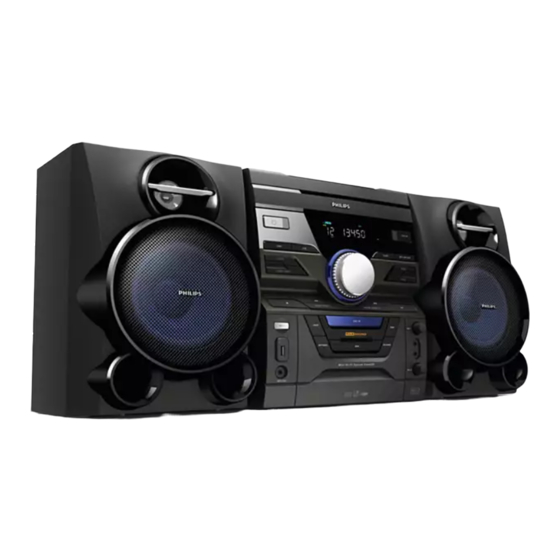
Philips FWM653 Service Manual
400w subwoofer mini hi-fi system
Hide thumbs
Also See for FWM653:
- Service manual (28 pages) ,
- User manual (24 pages) ,
- Quick start manual (2 pages)
Advertisement
Quick Links
Download this manual
See also:
User Manual
400W Subwoofer Mini Hi-Fi System
CONTENTS
Technical specification ..................................................................1-2
Version variation ...........................................................................1-2
Service measurement setup..........................................................1-3
Service aids .................................................................................1-4
Instructions on CD playability ................................................2-1..2-2
Block diagram ................................................................................3-1
Wiring diagram ..............................................................................4-1
Disassembly diagram............ ................................................5-1..5-2
Tuner board
Circuit diagram .........................................................................6-1
Layout diagram .........................................................................6-2
Main board
Circuit diagram .........................................................................7-1
Layout diagram ..................................................................7-2..7-3
Front board
Circuit diagram .........................................................................8-1
Layout diagram ..................................................................8-2..8-3
©
Copyright 2010 Philips Consumer Electronics B.V. Eindhoven, The Netherlands
All rights reserved. No part of this publication may be reproduced, stored in a retrieval
system or transmitted, in any form or by any means, electronic, mechanical, photocopying,
or otherwise without the prior permission of Philips.
Published by LX 1024 Service Audio
Version 1.0
Subject to modification
AMP Board
Circuit diagram. ........................................................................9-1
Layout diagram ..................................................................9-2..9-3
CD board
Circuit diagram .......................................................................10-1
Layout diagram ..............................................................10-2..10-3
MCU Board
Circuit diagram. ...................................................................... 11-1
Layout diagram .............................................................. 11-2..11-3
Exploded view diagram ...............................................................12-1
FWM653
-/55/77/BK
3141 785 35320
Advertisement

Related Manuals for Philips FWM653


Summary of Contents for Philips FWM653
- Page 1 Layout diagram ..............8-2..8-3 © Copyright 2010 Philips Consumer Electronics B.V. Eindhoven, The Netherlands All rights reserved. No part of this publication may be reproduced, stored in a retrieval system or transmitted, in any form or by any means, electronic, mechanical, photocopying, or otherwise without the prior permission of Philips.
-
Page 2: Technical Specification
• Speaker Width: 209 mm Connectivity Power • Audio Connections: RCA Aux in, 3.5mm stereo • Power supply: 100-240VAC, 50/60Hz • VERSION VARIATION Type /Versions: FWM653 Service policy Board in used: MAIN BOARD TUNER BOARD AMP BOARD FRONT BOARD CD BOARD... - Page 3 MEASUREMENT SETUP Tuner FM Bandpass LF Voltmeter 250Hz-15kHz e.g. PM2534 e.g. 7122 707 48001 RF Generator e.g. PM5326 S/N and distortion meter e.g. Sound Technology ST1700B Use a bandpass filter to eliminate hum (50Hz, 100Hz) and disturbance from the pilottone (19kHz, 38kHz). Tuner AM (MW,LW) Bandpass LF Voltmeter...
-
Page 4: Service Aids
SERVICE AIDS WARNING All ICs and many other semi-conductors are susceptible to electrostatic discharges (ESD). Careless handling during repair can reduce life drastically. When repairing, make sure that you are connected with the same potential as the mass of the set via a wrist wrap with resistance. Keep components and tools also at this potential. - Page 5 2 - 1 INSTRUCTIONS ON CD PLAYABILITY Customer complaint "CD related problem" Set remains closed! check playability playability ok ? For flap loaders (= access to CD drive possible) "fast" lens cleaning cleaning method is recommended check playability playability ok ? Play a CD for at least 10 minutes check playability...
- Page 6 2 - 2 INSTRUCTIONS ON CD PLAYABILITY PLAYABILITY CHECK LIQUID LENS CLEANING Before touching the lens it is advised to clean the surface of the lens by blowing clean air over it. For sets which are compatible with CD-RW discs This to avoid that little particles make scratches on use CD-RW Printed Audio Disc ....7104 099 96611 the lens.
-
Page 7: Block Diagram
BLOCK DIAGRAM TUNER SI4730 OR 3CDC ET8862Q& SENSOR TUENR PART PACK 3CD LOADER RC5/RC6 CODE 3CDC MOTOR DRIVER DRIVER IC BA5826 TDA7073A PICK UP 8M SERIAL CONTROL DATA MOTOR FALSH CD SERVO EN25T80 BU9543 BX8804 16M SDRAM CD PCM 128pin QFP BCK,LRCK, DATE USB/SD... -
Page 8: Wiring Diagram
WIRING DIAGRAM USB BOARD 2P/200MMCN551 TO 3CDC CON1 OPEN/CLOSE CD BOARD 4P/220MM CW104 TO CN904 5P/200MM(AA) CN504 TO CON2 3CD LOADER 6P/200MM CN505 TO CD MOTOR MCU BOARD PICK UP 28P/80MM(AA) CW101 TO CON589 MOTOR 16P/170MM(AA) CN501 TO CD RF 18P/130MM(AA)... - Page 11 CIRCUIT DIAGRAM - TUNER BOARD...
-
Page 12: Layout Diagram
LAYOUT DIAGRAM - TUNER BOARD... - Page 13 CIRCUIT DIAGRAM - MAIN BOARD...
- Page 14 PCB LAYOUT - MAIN BOARD TOP SIDE...
- Page 15 CIRCUIT DIAGRAM - MAIN BOARD BOTTOM SIDE...
- Page 16 CIRCUIT DIAGRAM - DISPLAY/KEY BOARD KEY1 C9065 4N7 C9013 R9023 10K 0.47/50V C9017 MIC-OUT R9026 SW901 C9009 470N 10U/16V SW911 R9007 SW921 VCC10V CN908 R9011 VR901 STOP C9014 R9025 DISPAY Q971 R9009 50K x2 100P C9007 BC857B 330K AGND L9005 L9001 SW902 SW912...
- Page 17 LAYOUT DIAGRAM - DISPLAY/KEY BOARD TOP SIDE...
- Page 18 LAYOUT DIAGRAM - DISPLAY/KEY BOARD BOTTOM SIDE...
- Page 19 CIRCUIT DIAGRAM - AMP BOARD...
- Page 20 LAYOUT DIAGRAM - AMP BOARD TOP SIDE...
- Page 21 LAYOUT DIAGRAM - AMP BOARD BOTTOM SIDE...
- Page 22 10-1 10-1 CIRCUIT DIAGRAM-CD BOARD...
- Page 23 10-2 10-2 LAYOUT DIAGRAM-CD BOARD TOP SIDE...
- Page 24 10-3 10-3 LAYOUT DIAGRAM-CD BOARD BOTTOM SIDE...
- Page 25 11-1 11-1 CIRCUIT DIAGRAM-MCU BOARD...
- Page 26 11-2 11-2 LAYOUT DIAGRAM-MCU BOARD TOP SIDE...
- Page 27 11-3 11-3 LAYOUT DIAGRAM-MCU BOARD BOTTOM SIDE...
- Page 28 12-1 12-1 SET EXPLODED VIEW...