Table of Contents
Advertisement
Quick Links
Advertisement
Table of Contents

Related Manuals for LG KG271


Summary of Contents for LG KG271
- Page 1 Service Manual KG271/KG276 Date: June, 2007 / Issue 1.0...
-
Page 2: Table Of Contents
Table Of Contents 1. INTRODUCTION .......5 4.13 Headphone Trouble ......75 4.14 Charging Trouble .........77 1.1 Purpose ..........5 4.15 FM Radio Trouble ........79 1.2 Regulatory Information......5 5. DOWNLOAD........82 2. PERFORMANCE.......7 5.1 Download Setup........82 2.1 H/W Features...........7 5.2 Download Process .........83 2.2 S/W Features ...........8 6. - Page 3 - 4 -...
-
Page 4: Introduction
1. INTRODUCTION 1. INTRODUCTION 1.1 Purpose This manual provides the information necessary to repair, description and download the features of this model. 1.2 Regulatory Information A. Security Toll fraud, the unauthorized use of telecommunications system by an unauthorized part (for example, persons other than your company’s employees, agents, subcontractors, or person working on your company’s behalf) can result in substantial additional charges for your telecommunications services. - Page 5 1. INTRODUCTION E. Notice of Radiated Emissions This model complies with rules regarding radiation and radio frequency emission as defined by local regulatory agencies. In accordance with these agencies, you may be required to provide information such as the following to the end user. F.
-
Page 6: Performance
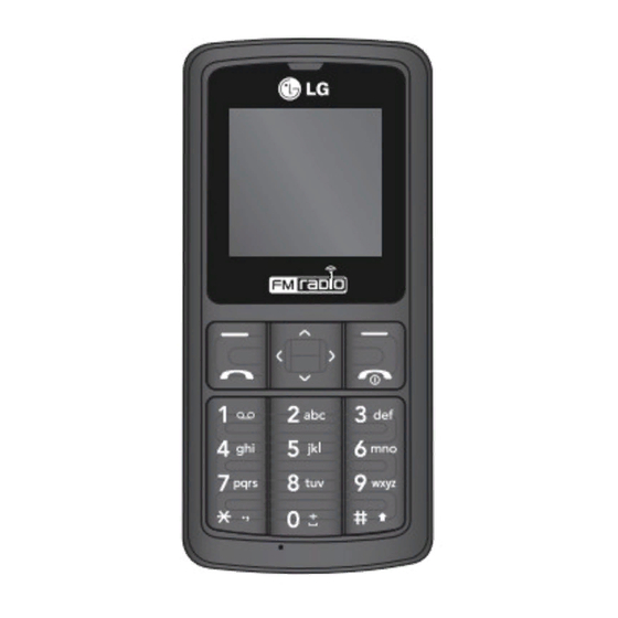
2. PERFORMANCE 2. PERFORMANCE 2.1 H/W Features Item Specifications Band GSM DUAL Band(900/1800) Type Bar type Dimension 98 * 45 * 12.9mm Weight Battery 750mAh Li-ion Talk Time Over 2hours @EGSM,TX Level : 5 Stand-by Time Over 200 hours @Paging period : 5 Under 4 hours when removed battery. -
Page 7: S/W Features
2. PERFORMANCE 2.2 S/W Features Function Detail Item Specification Etc. Operating System OS Data Circuit Packet Connectivity Infrared (IrDA) Bluetooth USB Mass storage RS232 Voice Function Voice Recording Voice Command Answering machine Memory User Memory Under 300KB Pictures (Still Image & Moving Image) MP3 (Music Contents) Java Contents... - Page 8 2. PERFORMANCE Function Detail Item Specification Etc. Display RSSI 6 level Battery Level 5 level Multi?Language Basic:English Max. 4 language of Latin 2 or 3 language of etc. Quick Access Mode PLMN/Service Indicator Dimming Clock Dual Clock Local Time / Selected Area Time Normal Features Last Dialed Number Last Received Number...
- Page 9 2. PERFORMANCE Function Detail Item Specification Etc. Network Automatic Network Selection Manual Network Selection Network Service Status DTMF DTMF Signaling DTMF Enable & Disable Audio Key Tone Volume 6 Level (Include Mute) Ring Tone Volume 6 Level (Include Mute) Ring Tone Pattern 10Type(fixed) Ring Type Silent Vibrator &...
- Page 10 2. PERFORMANCE Function Detail Item Specification Etc. Supp. Services Call Forwarding All Incoming Calls, No Reply On Busy, Not reachable Call Barring All Outgoing Calls, International Calls, Calls except to Home Country incoming Calls, All incoming Calls when roaming Conference Call up to 3 calls Plug?In Type 3 V only...
- Page 11 2. PERFORMANCE Function Detail Item Specification Etc. Sound contents Ringtones Karaoke Stutter Sound Flip tone Button tone Others Miscellaneous Development & Test Facility Function Field Test Facility Display Software Version IMEI Text Input Language Selectable Auto Language Predictive word input Scheduler Schedule 20 input (20 character)
- Page 12 2. PERFORMANCE Function Detail Item Specification Etc. Handset Restore Factory Setting Read Software Version Battery Charging Mode Security Emergency Call Handset Lock Security Code Delete all SIM Lock Key guard Real Time Clock 12/24 hour Calendar Automatic Leap Year Adjustment Time Zone Daylight saving Alarm Manager...
-
Page 13: Technical Brief
3. TECHNICAL BRIEF 3. TECHNICAL BRIEF 3.1 Digital Main Processor(PMB7880) Figure. 3-1 PMB7880 FUNCTIONAL BLOCK DIAGRAM - 14 -... - Page 14 3. TECHNICAL BRIEF 3.1.1 Overview of E-GOLDvoice The E-GOLDvoice is a GSM baseband modem including RF transceiver covering the low bands GSM850 /GSM900 and high bands GSM1800 / GSM1900 bands. E-GOLDvoice is Dual Band, therefore, it supports by default a low / high pair of bands at the same time: 1.
- Page 15 3. TECHNICAL BRIEF 3.1.2 Features ] Baseband • High performance fixed-point TEAKlite DSP • C166S high performance microcontroller • There are several Interfaces: - I2S interface for DAI connections (for Tape Approval) - High Speed SSC Interface for connection of external peripherals - SIM Interface - Keypad Interface (6x4 or 5x5 keys) - EBU for external RAM/FLASH connection...
- Page 16 3. TECHNICAL BRIEF ] Mixed Signal and Power Management Unit • DC/DC boost for voltages up to 15V for driving White or Blue LEDs • 8-Ohm loud speaker driver (250/350mW) • 16-Ohm earpiece driver • 32-Ohm headset driver • 4 measurement interfaces (PA temperature, battery voltage, battery temperature,and ambient temperature) •...
- Page 17 3. TECHNICAL BRIEF 3.1.3 GSM System Description The E-GOLDvoice is suited for mobile stations operating in the GSM850/900/1800/1900 bands. In the receiver path the antenna input signal is converted to the baseband, filtered, and then amplified to target level by the RF transceiver chipset. Two A-to-D converters generate two 6.5 Mbit/s data streams.
- Page 18 3. TECHNICAL BRIEF 3.1.4 PMU Details The E-GOLDvoice includes battery charger support (various sensor connections for temperature, battery technology, voltage, etc.) and a ringer buffer. E-GOLDvoice avoids the need for an external power management component because its internal power management unit contains: •...
-
Page 19: Power Management
3. TECHNICAL BRIEF 3.1.12 C166 Debug Concept The debugging of the C166 uses the OCDS and the Cerberus. 3.1.13 TEAKLite Debug Concept TEAKlite debugging uses the OCEM and the SEIB. 3.1.14 Power Management The E-GOLDvoice provides the power management unit (PMU) for the complete mobile phone application. - Page 20 3. TECHNICAL BRIEF The security features use the following mechanism: • Boot ROM flow: - Controls the boot transition to external flash - Controls the flash update • Flash tied to the individual chip via an ID using e-fuses, that is, each E-GOLDvoice chip has its own fused ID.
-
Page 21: Power Amplifier Module (Sky77318)
3. TECHNICAL BRIEF 3.2 Power Amplifier Module (SKY77318) Figure. 3-2 SKY77318 FUNCTIONAL BLOCK DIAGRAM The SKY77318 Power Amplifier Module (PAM) is designed in a low profile (1.2 mm), compact form factor for quad-band cellular handsets comprising GSM850/900, DCS1800, and PCS1900 operation. The PAM also supports Class 12 General Packet Radio Service (GPRS) multi-slot operation. - Page 22 3. TECHNICAL BRIEF RF input and output ports of the SKY77318 are internally matched to a 50 Ω load to reduce the number of external components for a quad-band design. Extremely low leakage current (2.5 µA, typical) of the dual PA module maximizes handset standby time. The SKY77318 also contains bandselect switching circuitry to select GSM (logic 0) or DCS/PCS (logic 1) as determined from the Band Select (BS) signal.
-
Page 23: 26 Mhz Clock (Dcxo)
3. TECHNICAL BRIEF 3.3 26 MHz Clock (DCXO) Figure. 3-3 E-GoldVoice DCXO Overview DCXO (Digitally Controlled Crystal Oscillator) and VCTCXO (Voltage Controlled Temperature Compensated Crystal Oscillator) are two different techniques used To maintain the mobile’s reference oscillator’s accuracy over time. The reference oscillator’s accuracy over time will vary due to initial crystal frequency offset, temperature drift and aging. -
Page 24: Rtc(32.768Khz Crystal)
3. TECHNICAL BRIEF 3.4 RTC(32.768KHz Crystal) 32.768KHZ CRYSTAL X100 32KIN 32KOUT MC-146_12_5PF 32.768KHz Figure. 3-4 E-Gold Voice RTC Interface The integrated Real Time Clock (RTC) is able to provide programmable alarm functions and external interrupts. Due to its extreme low power consumption the RTC can be supplied from a small backup battery. -
Page 25: Lcd Interface(3-Wire Spi Interface)
3. TECHNICAL BRIEF 3.5 LCD Interface(3-wire SPI interface) 2V8_VIO CN200 MTPD MTPG R205 LCD_RESET R206 R207 SSC0_CLK R208 SSC0_MTSR MLED MLED1 MLED2 C211 C212 C213 C214 C208 C209 C210 LCD_ID R210 C221 100K IMSA-9671S-13Y902 (ENQY0013801) Figure 3-5-1. LCD Interface VBAT CHARGE PUMP U200 AAT3157ITP-T1... - Page 26 3. TECHNICAL BRIEF Signals Description This signal enable to access to the driver IC of LCD. SSC0_MTSR This signal transfer serial data to driver IC. SSC0_CLK This signal transfer serial clock to driver IC. LCD_RESET This signal makes driver IC to HW default status. MLED This signal provide power to white LEDs.
-
Page 27: Sim Card Interface
3. TECHNICAL BRIEF 3.6 SIM Card Interface 2V85_VSIM 2V85_VSIM 2V85_VSIM J300 SIM_RST SIM_DATA SIM_CLK GND2 GND1 C310 C311 C312 0.1u Figure 3-6. SIM CARD Interface The EGoldVoice provides SIM Interface Module. The AD6527 checks status Periodically During established call mode whether SIM card is inserted or not, but it doesn't check during deep sleep mode. -
Page 28: Keypad Interface
3. TECHNICAL BRIEF 3.7 KEYPAD Interface 2V0_VRTC KEY MATRIX SW200 END_KEY LEFT SW201 SW202 SW203 SW204 SW205 MENU R201 KEY_OUT1 C205 SW206 SW207 SW208 SW209 SW210 R203 KEY_OUT2 C206 SW211 SW212 SW213 SW214 SW215 RIGHT SEND R204 KEY_OUT3 C207 SW216 SW217 SW218 SW219... -
Page 29: Battery Charging Block Interface
3. TECHNICAL BRIEF 3.8 Battery Charging Block Interface CHARGING IC 2V8_VIO VCHARGE VBAT VCHARGE R118 U101 R119 1.8K CHARGE_DETECT VBAT C125 R120 _FAULT VSEN_TEMP (10V,K,X5R) R121 CHG_STATUS _STATUS IREF R122 CHG_EN_TEST C126 TIME V2P8 (10V,K,X5R) R123 CHG_EN C127 PGND 0.015u C128 R124 R125... -
Page 30: Rf Interface
3. TECHNICAL BRIEF 3.9 RF Interface FL400 LMSP2PAA-575TEMP GSM1800_1900TX GSM1800_1900RX VC_GSM850_900TX VC_GSM1800_1900TX C417 C418 GND1 GSM850_900TX GND2 GSM850_900RX GND3 Figure 3-9-1. ASM interface C419 GSM_RXN L403 18nH 5 10 O2_2 C420 GSM_RXP O2_1 O1_2 C421 DCS_RXN O1_1 FL401 B9308 L404 PART_NO SFSB0001401 5.1nH IN CASE OF GSM850/PCS1900... - Page 31 3. TECHNICAL BRIEF VBAT VBAT R404 R405 DCS_PCS_OUT L402 C402 C403 C404 C405 C406 C407 C408 0.01u 0.01u (2012) C409 (50V,J,NP0) (16V,K,X7R) DCS_PCS_OUT DCS_PCS_IN R406 R407 U400 EGSM_OUT EGSM_IN GSM_OUT SKY77318 C411 C412 RSVD_GND ENABLE TXON_PA R409 R408 P_GND C413 C414 R410 C416...
-
Page 32: Audio Interface
3. TECHNICAL BRIEF 3.10 Audio Interface VMIC LOUD2 SPK_N LOUD1 SPK_P VMIC MICP2 AUXIP C124 MICN2 AUXIN 1000p MICP1 VINNORP MICN1 VINNORN EPPA1 EPPA1 EPP1 REC_P EPN1 REC_N Figure 3-10-1 Audio interface The audio front-end of E-GOLDvoice offers the digital and analog circuit blocks for both receive and transmit audio operation and ringing. - Page 33 3. TECHNICAL BRIEF The interface to the processor cores consists of a direct physical connection to the TEAKlite DSP bus and a set of firmware commands to handle communication between the C166S and the audio front- end which serves as the interface peripheral for audio algorithms running on the DSP or the controller. The audio front-end Generates interrupts on certain occasions, for example, when exchange of data is requested.
- Page 34 3. TECHNICAL BRIEF RECEIVER CN100 L100 22nH REC_P L101 22nH C100 11*07*3T receiver REC_N (SURY0013001) C102 C103 Figure 3-10-2 Main Receiver interface SPEAKER SPEAKER AMPLIFIER R102 VBAT R103 C116 CN101 U100 NCP2890AFCT2G L103 27nH R104 C117 0.1u SPK_N OUTB L104 27nH OUTA R105...
- Page 35 3. TECHNICAL BRIEF VMIC MAIN_MIC R300 R301 C303 C304 2.2K R304 C306 0.1u VINNORP OB4-15L42-C33L 100ohm C308 C307 0.1u R307 C309 0.1u MIC300 VINNORN 100ohm R309 2.2K Figure 3-10-4 Main Microphone interface VMIC C317 R318 AUXIN EAR_MIC 2.2K 0.1u C318 C319 I/O CONNECTOR C320...
-
Page 36: Key Led Interface
3. TECHNICAL BRIEF 3.11 Key LED Interface VBAT KEY BACKLIGHT (10V,K,X5R) (10V,K,X5R) R222 2SC5585 KEY_BACKLIGHT Q200 R223 Figure 3-11 Key LED interface This handset has 6 LEDs that illuminates blue color. Control signal is controlled by EGold-voice with PWM and handset has 3 methods, ON, OFF and Dimming. -
Page 37: Vibrator Interface
3. TECHNICAL BRIEF 3.12 Vibrator Interface VIBRATOR VBAT VBAT C302 (50V,J,NP0) CN300 C305 R305 (1608) R306 Q300 VIBRATOR 2SC5585 Figure 3-12 Vibrator interface This handset has vibrator operation. Control signal is controlled by EGold-voice with PWM. - 38 -... -
Page 38: Memory Interface
3. TECHNICAL BRIEF 3.13 Memory Interface VBAT 2V8_VMEM_S (NOT MOUNTED) U300 BH28FB1WHFV STBY BGND VOUT MEMORY C300 C301 U301 S71GL032A40BAW0F ADD01 DATA00 ADD02 DATA01 ADD03 DATA02 ADD04 DATA03 ADD05 DATA04 ADD06 DATA05 ADD07 DATA06 ADD08 DATA07 ADD09 DATA08 ADD10 DATA09 ADD11 DATA10 DQ10... -
Page 39: Power Block Interface
3. TECHNICAL BRIEF 3.14 Power Block Interface 3V2_VBUF VRF1 (1608) 2V0_VRTC C111 R100 6.8K BAT100 C113 L102 18nH VBAT C115 (1608) 2.2u (16V,K,X5R) REXT Figure 3-14-1 Power Block interface The E-GOLDvoice integrated power management unit (PMU) supports direct connection to battery (DCB). - Page 40 3. TECHNICAL BRIEF Name Output Voltage(V) Output Current (mA) Comment LRTC Used for the real time and digital PMU supply 1.2/1.5 Used for the core supplies (MCU and DSP via switch) 1.8/2.85 Used for the I/O pad supply and, for example, the display LRFXO Used for the crystal oscillator supply LMEM...
-
Page 41: Fm Radio Interface
3. TECHNICAL BRIEF 3.15 FM Radio Interface - 42 -... -
Page 42: Headphone Amplifier
3. TECHNICAL BRIEF 3.15.1 FM Tunner The Si4702 patented digital low-IF architecture reduces external components and eliminates the need for factory adjustments. The receive (RX) section integrates a low noise amplifier (LNA) supporting the worldwide FM broadcast band (76 to 108 MHz). An automatic gain control (AGC) circuit controls the gain of the LNA to optimize sensitivity and rejection of strong interferers. -
Page 43: Trouble Shooting
4. TROUBLE SHOOTING 4. TROUBLE SHOOTING 4.1 RF Trouble SW400 FL400 FL401 U400 U102 X101 REFERENCE PART Description U400 PAM (Power Amp. Module) X101 DCXO (26MHz) FL400 ASM (Antenna Switch Module) SW400 Mobile Switch FL401 RX SAW Filter - 44 -... - Page 44 4. TROUBLE SHOOTING RF Trouble TEST POINT Antenna Matching component Antenna.Contact Point SW400 TP400 TP401 TP402 TP403 TP404 TP405 CIRCUIT DIAGRAM R400 R401 C400 Antenna Matching component L401 22nH SW400 RF500 Mobile SW Coupling Capacitor C410 - 45 -...
- Page 45 4. TROUBLE SHOOTING CHECKING FLOW START Check Antenna PAD& Change Antenna Intenna Contact Check Resolder component Matching component Check Change SW400 Mobile SW Download Calibration Change PCB - 46 -...
- Page 46 4. TROUBLE SHOOTING RX Trouble TEST POINT CHECKING FLOW START Setup Test Equipment Cell Power :-74d Bm SW400 GSM850 CH190 PCS CH660 FL400 Check point. DCXO(X101) FL401 U400 Check point mobile SW & ASM & SAW Filter(SW400,F L400,FL401) U102 X101 Re-Download S/W &...
- Page 47 4. TROUBLE SHOOTING RX Trouble (1) Checking VCTCXO Circuit TEST POINT CHECKING FLOW Is the waveform of Pin3 similar to Replace DCXO(X101) X101 Waveform? SW400 FL400 DCXO Circuit is OK. See next page to check PLL Circuit. FL401 U400 U102 X101 CIRCUIT Waveform...
- Page 48 4. TROUBLE SHOOTING RX Trouble TEST POINT CHECKING FLOW Check Pin 1, 2 of SW400 with RF Cable Replace SW400 Signal is Mobile SW OK ? (SW400) FL400 Pin 6 Pin 4 Check Pin 4,6 of Replace ASM FL400 ? FL401 (FL400) U400...
-
Page 49: Tx Trouble
4. TROUBLE SHOOTING 4.2 TX Trouble TEST POINT CHECKING FLOW Setup Test Equipment Cell Power : - 74dBm GSM850 CH190 PCS CH661 Check point SW400 DCXO(X101) Check point FL400 ULC2(U102)Outp ut Signal FL401 U400 Check point PAM(U400) Control Signal Check ASM &... - Page 50 4. TROUBLE SHOOTING TX Trouble TEST POINT CIRCUIT VBAT VBAT R404 R405 DCS_PCS_OUT U400 L402 C402 C403 C404 C405 C406 C407 C408 0.01u 0.01u (2012) C409 LB RF Input (50V,J,NP0) (16V,K,X7R) DCS_PCS_OUT DCS_PCS_IN R406 R407 U400 EGSM_OUT EGSM_IN GSM_OUT SKY77318 C411 C412 RSVD_GND...
- Page 51 4. TROUBLE SHOOTING TX Trouble TEST POINT CIRCUIT TP400 TP401 TP402 TP403 TP404 TP405 R400 R401 C400 SW400 L401 22nH FL400 SW400 FL401 RF500 U400 C410 U102 X101 FL400 LMSP2PAA-575TEMP GSM1800_1900TX GSM1800_1900RX VC_GSM850_900TX VC_GSM1800_1900TX C417 C418 GND1 GSM850_900TX GND2 GSM850_900RX GND3 Mode GSM900 TX...
- Page 52 4. TROUBLE SHOOTING RX Trouble TEST POINT CHECKING FLOW Check Pin 1, 2 of SW400 with RF Cable Replace Mobile Signal is SW400 SW (SW400) OK ? FL400 Pin 1 Pin 7 Check Pin 1,2 Pin 2 FL401 U400 Pin 3 Control Check ULC2 Signal is...
-
Page 53: Power On Trouble
4. TROUBLE SHOOTING 4.3 Power On Trouble TEST POINT Check Points C107 -Battery Voltage( Need to over 3.35V) -Power-On Key detection (PWRON signal) C111 C101 -Outputs of LDOs from EGV VOLTAGE PART C109 C110 V_BUF 3.2V C101 V_MEM 2.8V C109 C106 V_IO 2.8V... - Page 54 4. TROUBLE SHOOTING Power On Trouble CHECKING FLOW START Check Battery Voltage Charge or Change Battery > 3.35V Push power-on key Check the contact of power key And check the level change Or dome-switch of PWRKEY Check the voltage of Replace U102 The LDO outputs at U102 VOLTAGE...
-
Page 55: Sim Card Trouble
4. TROUBLE SHOOTING 4.4. SIM Card Trouble TEST POINT R302/C310 J300.PIN1 C331/C332 CIRCUIT DIAGRAM 2V85_VSIM 2V85_VSIM 2V85_VSIM J300 SIM_RST SIM_DATA SIM_CLK GND2 GND1 C310 C311 C312 0.1u - 56 -... - Page 56 4. TROUBLE SHOOTING Checking Flow START Does the SIM cards Change the SIM Card. Our phone supports 3V ? supports only 3V SIM card. Check soldering Resolder J300 or R302/C310/ status of J300 and other component Other component C311/C312 J300.PIN1 = 2.85V Check J300.PIN1 Change board Re-download SW...
-
Page 57: Vibrator Trouble
4. TROUBLE SHOOTING 4.5. Vibrator Trouble TEST POINT Q300.PIN3 R306 R308 R305 CIRCUIT DIAGRAM VBAT VBAT C302 (50V,J,NP0) CN300 C305 R305 (1608) R306 Q300 VIBRATOR 2SC5585 - 58 -... - Page 58 4. TROUBLE SHOOTING Checking Flow START Enter the engineering mode, and set vibrator on. R306=2.8V Check Voltage Level of Change PCB R308=0.7V R306/R308 Q300.PIN3=0V Check Voltage Level of Change Q300 R305=0V Q300.PIN3 and R305 Replace Vibrator - 59 -...
-
Page 59: Keypad Trouble
4. TROUBLE SHOOTING 4.6. Keypad Trouble TEST POINT R215 R214 R201 R211 R212 R203 R209 R213 R204 CIRCUIT DIAGRAM 2V0_VRTC KEY MATRIX SW200 END_KEY LEFT SW201 SW202 SW203 SW204 SW205 MENU R201 KEY_OUT1 C205 SW206 SW207 SW208 SW209 SW210 R203 KEY_OUT2 C206 SW211... - Page 60 4. TROUBLE SHOOTING Checking Flow START Check Metal Doom Change Metal Doom R201/R203/R204 R209/R211/R212 Check soldering status Resolder component R213/R214/R215 Of component Change PCB - 61 -...
-
Page 61: Rtc Trouble
4. TROUBLE SHOOTING 4.7 RTC Trouble CIRCUIT Check Points - 32.768KHz is right clock - The power of RTC is right. SWITCH_ON PWRON OSC32K 32KOUT F32K 32KIN CLKOUT CHG_STATUS X100 R100 32KIN 6.8K BAT100 32KOUT MC-146_12_5PF 32.768KHz - 62 -... - Page 62 4. TROUBLE SHOOTING CHECKING FLOW START Is the frequency Replace X100 and try again. about 32Khz? Is VRTC Replace BAT100 about 2.0V? RTC will work properly - 63 -...
-
Page 63: Key Backlight Trouble
4. TROUBLE SHOOTING 4.8. Key backlight Trouble TEST POINT D203 D200 Q200.PIN3 R204 D20 4 D201 R203 Q200.PIN2 D205 D202 CIRCUIT DIAGRAM VBAT KEY BACKLIGHT (10V,K,X5R) (10V,K,X5R) R222 2SC5585 KEY_BACKLIGHT Q200 R223 - 64 -... - Page 64 4. TROUBLE SHOOTING Checking Flow START Check Voltage Level Change PCB R222=2.8V Of R222 Replace component Check Voltage Level Check component R222=0.7V Of R222 and Q200.PIN2 R222 and Q200 Check LED Replace component LD200~LD205 component R216~R221 Change PCB - 65 -...
-
Page 65: Lcd Trouble
4. TROUBLE SHOOTING 4.9. LCD Trouble TEST POINT CN200 R207 R205 R206 R208 C221 CIRCUIT DIAGRAM 2V8_VIO CN200 MTPD MTPG R205 LCD_RESET R206 R207 SSC0_CLK R208 SSC0_MTSR MLED MLED1 MLED2 C211 C212 C213 C214 C208 C209 C210 LCD_ID R210 C221 100K IMSA-9671S-13Y902 (ENQY0013801) - Page 66 4. TROUBLE SHOOTING Checking Flow START Change PCB Backlight is OK? Check Operation Change LCD After LCD changes C221=2.8V Check Control Replace component Signal and Power Control Signal= Or change PCB Including soldering status Refer to next page Check soldering Replace CN200 status of CN200 Change PCB...
- Page 67 4. TROUBLE SHOOTING WAVEFORM SS0_SCK LCD_CS ]SS0_MTSR pattern is out randomly when clock is fluctiatied. , clock frequency is 13MHz and LCD_RESET is High(2.8V). - 68 -...
-
Page 68: Microphone Trouble
4. TROUBLE SHOOTING 4.10. Microphone Trouble TEST POINT Microphone component R300 MIC.P CIRCUIT DIAGRAM VMIC MAIN_MIC R300 R301 C303 C304 2.2K R304 C306 0.1u VINNORP OB4-15L42-C33L 100ohm C308 C307 0.1u R307 C309 0.1u MIC300 VINNORN 100ohm R309 2.2K - 69 -... - Page 69 4. TROUBLE SHOOTING Checking Flow Make a call R300.VMIC=2.5V Check voltage level Replace PCB of R300 Re-solder or Check component replace the Component status around MIC Re-solder or Check status of MIC replace Microphone Check the voltage Level Change Microphone of MIC_P MIC_P= about 1.2~1.5V DC with a few tens mV...
-
Page 70: Receiver Trouble
4. TROUBLE SHOOTING 4.11. Receiver Trouble TEST POINT L101 L100 C103 C102 REC.N REC.P CIRCUIT DIAGRAM RECEIVER CN100 L100 22nH REC_P L101 22nH C100 11*07*3T receiver REC_N (SURY0013001) C102 C103 - 71 -... - Page 71 4. TROUBLE SHOOTING Checking Flow Press any Key Check L100/L101 Re-solder or Check component C102/103 replace the Component status L100&L101 bias will Re-solder or Check L100 & Fluctiate signal above replace the Component L101 1.2V replace Receiver Check Receiver Replace PCB - 72 -...
-
Page 72: Speaker Trouble
4. TROUBLE SHOOTING 4.12 Speaker Trouble TEST POINT Check Points L103 - Speaker spring contact - Audio amp soldering L104 CN101íS 1PIN CN101íS 2PIN C120 CN200 AMP IC C117 R111 C118 CIRCUIT SPEAKER SPEAKER AMPLIFIER R102 VBAT R103 C116 CN101 U100 NCP2890AFCT2G L103... - Page 73 4. TROUBLE SHOOTING Checking Flow Start Check Check the voltage level The battery of U100 = Vbat? Check Check the Signal, U102 C117,C118 Check the Level of Check U100.C3 = Low ? U102 Re-solder Check the Signal, L102,L103 L102,L103 Re-Assemble Check the Contact or Re-place Of CN101...
-
Page 74: Headphone Trouble
4. TROUBLE SHOOTING 4.13 Headphone Trouble TEST POINT Check Points C321 -18pin IO connector CN301 C322 -Passive Parts slodering Status FB300 FB302 FB301 CIRCUIT DIAGRAM VMIC C317 R318 AUXIN EAR_MIC 2.2K 0.1u C318 C319 I/O CONNECTOR C320 0.1u AUXIP FM_ANT VBAT L300 CN301... - Page 75 4. TROUBLE SHOOTING CHECKING FLOW START Does the audio profile of the phone Re-solder CN301 or Change Check the voltage Level change to the another Ear- Mic set and Try again CN301.8 = Low? earphone mode? Replace U100 or Change Board Earphone Go to MIC Trouble section...
-
Page 76: Charging Trouble
4. TROUBLE SHOOTING 4.14 Charging Trouble TEST POINT R124 Charger Check Points U101 -Connection of TA (check TA voltage 5.2V) -Charging Current Path component voltage drop C126 VCHARGE VBAT =5.2V -Battery voltage C125 -Charging IC CN301 CIRCUIT CHARGING IC 2V8_VIO VCHARGE VBAT VCHARGE... - Page 77 4. TROUBLE SHOOTING Checking Flow START Resolder the CN300 I/O Connector(CN301) Pin 12,13 : VCHARGE Is well-soldered ? The TA is out of order Is The Voltage of C126 Change the TA 5.2V ? Replace the The Voltage of C128 U101 Is 2.8V Check the voltage of R124...
-
Page 78: Fm Radio Trouble
4. TROUBLE SHOOTING 4.15. FM Radio Trouble TEST POINT R332 R338/R337/R336 U304.P 1 U304.P4 R327 R331 U302 U303 R329/R330 C332/C333 - 79 -... - Page 79 4. TROUBLE SHOOTING CIRCUIT DIAGRAM - 80 -...
- Page 80 4. TROUBLE SHOOTING Checking Flow Connector Headset and Turn on Radio and tuned channel U304.PIN1 = High Check LDO Change U304 U304.PIN4=2.8V Power Check R336/R337/338 Change PCB Control Signal Check I2C signal and 32K clock Check Audio Output Change U302 R329/R330 Of Transceiver C332/C333...
-
Page 81: Download
5. DOWNLOAD 5. DOWNLOAD 5.1 Download Setup Configure system like figure 5-1. Figure 9-1. Download Setup - 82 -... -
Page 82: Download Process
5. DOWNLOAD 5.2 Download Process 5.2.1. Download step[1] : Start or Stop download : Selected configuration DLL file : File name donwloading → Exit(X) : End program File(F) Setting(S) → Configuration : configuration download condition DLL, SW files and etc. About(H) →... - Page 83 5. DOWNLOAD 5.2.2. Download step[2] : Select a appropriated DLL file - You must select KG270_xxxxxx.DLL file. : Select configuration file You must select cmd.m0 file : Select download speed You must 460800. System supports maximum 460800bps. : Select port select start and end port be operated - 84 -...
- Page 84 5. DOWNLOAD 5.2.3. Download step[3] : Select files downloaded KG270 have 4 files, *.eep, *.fls, *.dffs and *.cust. But You must not select *.eep file. - 85 -...
- Page 85 5. DOWNLOAD 5.2.4. Download step[4] : Start download and stop download next step. If configuration is finished, then push start button and then button is changed to STOP. Turn on power of multi download and connector phones. If download is started, then push start button else program will download repeatedly. - 86 -...
- Page 86 5. DOWNLOAD 5.2.5. Download step[5] : This region appears donwload status. If download is finished, PASS or FAIL.message is showed. - 87 -...
-
Page 87: Block Diagram
6. BLOCK DIAGRAM 6. BLOCK DIAGRAM - 88 -... -
Page 88: Circuit Diagram
Date Sign & Name Sheet/ VBAT VBAT Sheets GB3_RADIO 11/16 MODEL SANG-YOEN.LEE Designer SPFY0144601 2006 VBAT1 VBAT2 GND1 GND2 Checked DRAWING NAME Approved DRAWING VER-1.1 LG Electronics Inc. Iss. Notice No. Date Name LG(42)-A-5505-10:01 LG Electronics Inc. - 89 -... - Page 89 R222 2SC5585 KEY_BACKLIGHT Section Date Sign & Name Sheet/ Q200 GB3_RADIO Sheets R223 MODEL 11/16 HYUN-OK.LEE Designer 2006 Checked DRAWING AUDIO,LCD,KEY NAME Approved DRAWING Iss. Notice No. Date Name REV-1.1 LG Electronics Inc. LGIC(42)-A-5505-10:01 LG Electronics Inc. - 90 -...
- Page 90 MODEL SANG-YEON.LEE C341 C342 HEADSET_RADIO_SEL Designer SPFY0144601 2006 RADIO_DETECT R345 (10V,K,X5R) 100K RADIO Checked 2006 NO RADIO 2.7K DRAWING RADIO,MEMORY,AUDIO,I/O NAME Approved 2006 DRAWING VER-1.1 LG Electronics Inc. Iss. Notice No. Date Name LG(42)-A-5505-10:01 LG Electronics Inc. - 91 -...
- Page 91 C422 DCS_RXP CHANGE THIS DUAL SAW FILTER TO PART_NO SFSB0001301 Section Date Sign & Name Sheet/Sheets GB3_RADIO MODEL 11/16 Designer KEE-OUN.PARK 2006 Checked DRAWING 2006 NAME Approved 2006 DRAWING VER-1.1 LG Electronics Inc. LGIC(42)-A-5505-10:01 LG Electronics Inc. - 92 -...
-
Page 92: Pcb Layout
8. PCB LAYOUT - 93 -... - Page 93 8. PCB LAYOUT - 94 -...
-
Page 94: Engineering Mode
9. ENGINEERING MODE 9. ENGINEERING MODE 9.1 About Engineering Mode Engineering mode is designed to allow a service man/engineer to view and test the basic functions provided by a handset. 9.2 Access Codes The key sequence for switching the engineering mode on is 2945#*#. Pressing END will switch back to non-engineering mode operation. - Page 95 9. ENGINEERING MODE BB TEST 1. Backlight 1. Backlight On 2. Backlight Off 3. Backlight Value 2. LCD 1. LCD Color 1. Red 2. Green 3. Blue 2. Contrast 4. Black 5. White 6. Auto LCD 3. Battery Info 1. Vibrator On 4.
-
Page 96: Bb Test
9. ENGINEERING MODE 9.4.1 BB Test 9.4.1.1 Backlight ➀ backlight on : LCD backlight is off. ➁ backlight off : LCD backlight is on. ➂ backlight value : LCD backlight brightness is controlled by 20% from 100 to 0. 9.4.1.2 LCD ➀... - Page 97 9. ENGINEERING MODE Model Version 9.4.2 Model Version This menu displays the Model software version. Eng Mode 1. Serving Cell 2. Neighbour Cells 3. Reset Information - 98 -...
-
Page 98: Eng Mode
9. ENGINEERING MODE 9.4.3 Eng Mode 9.4.3.1 Serving Cell This Menu dispays the the informations of Serving Cell environment. For example, ARFCN, RF Level etc. ARFCN : Absolut Radio Frequency Channel Number (Frequency Number) of Serving Cell while Idle mode RxLev : RX level of Serving Cell while Idle mode C1 : C1 Value of Serving Cell, This value will be used to decide cell reselection. - Page 99 9. ENGINEERING MODE 9.4.3.2 Neighbour Cells This menu displays the informations of Neighbour Cells. ARFCN : Absolut Radio Frequency Channel Number (Frequency Number) of Neighbour Cell RxLev : Rx Level of Neighbour Cell C1 : C1 Value of Neighbour Cell, This value will be used to decide cell reselection. C2 : C2 Value of Neighbour Cell, This value will be used to decide cell reselection.
-
Page 100: Call Timer
9. ENGINEERING MODE Call Timer 9.4.4 Call Timer This menu displays the time of all calls, including the received calls. Factory Reset 9.4.5 Factory Reset This menu is to format data block in the flash memory and this procedure set up the default value in data block. - Page 101 9. ENGINEERING MODE MF TEST 1. All auto Test 2. Backlight 3. Audio 4. Vibrator 5. LCD 6. Key Pad 7. Mic Speaker 8. FM radio * function is not supported - 102 -...
-
Page 102: Mf Test
9. ENGINEERING MODE 9.4.6 MF TEST This manufacturing mode is designed to do the baseband test automatically. Selecting this menu will process the test automatically, and phone displays the previous menu after completing the test. 9.4.6.1 All auto Test LCD, Backlight, Vibrator, Buzzer, Key Pad 9.4.6.2 Backlight LCD Backlight is on for about 1.5 seconds at the same time, then off. -
Page 103: Calibration
10. CALIBRATION 10. CALIBRATION 10.1 Test Equipment Setup 4.000V 0.0000A 10.2 Calibration Steps 10.2.1 Tune on the phone 10.2.2 Execute “HK_28.exe” - 104 -... - Page 104 10. CALIBRATION 10.2.3 Click “SETTING” Memu KG278 10.2.4 Setup “Ezlooks” menu such as the following fugure - 105 -...
- Page 105 10. CALIBRATION 10.2.5 Setup “Line System” menu such as the following fugure KG278 Adjust the number of times. 10.2.6 Setup Logic operation such as the following figure KG278 Operation Mode 1. By-Pass: not control by GPIB 2. Normal : control by GPIB Setup UART Port PWR : Power Supply CELL :Call-Test Equipment...
- Page 106 10. CALIBRATION 10.2.7 Select “MODEL” 10.2.8 Click “START” for RF calibration KG278 10.2.9 RF Calibration finish - 107 -...
- Page 107 10. CALIBRATION 10.2.10 Calibration data will be saved to the following folder - 108 -...
-
Page 108: Stand Alone Test
11. STAND ALONE TEST 11. STAND ALONE TEST 11.1 Test Program Setting 11.1.1 Set COM Port 11.1.2 Check PC Baud rate(115200) 11.1.3 Confirm EEPROM & Delta file prefix name 11.1.4 Click “V24AT#ON” and then “Update Info” for communicating Phone and Test Program Not Connected - 109 -... - Page 109 11. STAND ALONE TEST Connected 11.1.5 For the purpose of the Standalone Test, Change the Phone to “ptest mode” and then Click the “Reset” bar. 11.1.6 Select “Non signaling” in the Quick Bar menu. Then Standalone Test setup is finished. Change "ptest mode"...
-
Page 110: Tx Test
11. STAND ALONE TEST 11.2 Tx Test 11.2.1 Click “Non signaling mode” bar and then confirm “OK” test in the command line 11.2.2 Put the number of TX Channel in the ARFCN 11.2.3 Select “TX” in the RF mode menu and “PCL” in the PA Level menu 11.2.4 Finally, Click “Write All”... -
Page 111: Rx Test
11. STAND ALONE TEST 11.3 RX Test 11.3.1 Put the number of RX Channel in the ARFCN 11.3.2 Select “RX” in the RF mode menu 11.3.3 Finally, Click “Write All” bar and try the efficiency test of Phone - 112 -... -
Page 112: Exploded View & Replacement Part List
12. EXPLODED VIEW & REPLACEMENT PART LIST 12.1 EXPLODED VIEW - 113 -... - Page 113 - 114 -...
-
Page 114: Replacement Parts
COMPLEX, (empty), , , , , Color GMEY00 SCREW MACHINE,BIND GMEY0002001 1.4 mm,3 mm,MSWR3(BK) ,B ,+ ,HEAD t=0.6, HEAD d2.7 Without MBJA00 BUTTON,DIAL MBJA0024302 KG271 PAKBK Color MCCF00 CAP,MOBILE SWITCH MCCF0042301 MOLD, Urethane Rubber S185A, , , , , Black Without MLAK00 LABEL,MODEL... - Page 115 12. EXPLODED VIEW & REPLACEMENT PART LIST Location Level Description Part Number Specification Color Remark Without SC100 CAN,SHIELD MCBA0016401 PRESS, NS, 0.2, , , , Color - 116 -...
-
Page 116: Main Component
12. EXPLODED VIEW & REPLACEMENT PART LIST <Main component> Note: This Chapter is used for reference, Part order is ordered by SBOM standard on GCSC Location Level Description Part Number Specification Color Remark SJMY00 VIBRATOR,MOTOR SJMY0007903 3 V,0.85 A,4*8 ,Height 5.8T Cylinder ,; ,3V , , ,11000 , , , , VIBRATOR,MOTOR SJMY0007904 3 V,.1 A,4*8 ,height 5.8mm ,;... - Page 117 12. EXPLODED VIEW & REPLACEMENT PART LIST Location Level Description Part Number Specification Color Remark C122 CAP,CERAMIC,CHIP ECCH0000182 0.1 uF,10V ,K ,X5R ,HD ,1005 ,R/TP C123 CAP,CERAMIC,CHIP ECCH0000182 0.1 uF,10V ,K ,X5R ,HD ,1005 ,R/TP C124 CAP,CERAMIC,CHIP ECCH0000143 1 nF,50V,K,X7R,HD,1005,R/TP C125 CAP,CHIP,MAKER ECZH0001215...
- Page 118 12. EXPLODED VIEW & REPLACEMENT PART LIST Location Level Description Part Number Specification Color Remark C312 CAP,CERAMIC,CHIP ECCH0000115 22 pF,50V,J,NP0,TC,1005,R/TP C313 CAP,CERAMIC,CHIP ECCH0000120 39 pF,50V,J,NP0,TC,1005,R/TP C314 CAP,CERAMIC,CHIP ECCH0000120 39 pF,50V,J,NP0,TC,1005,R/TP C315 CAP,CERAMIC,CHIP ECCH0000182 0.1 uF,10V ,K ,X5R ,HD ,1005 ,R/TP C316 CAP,CERAMIC,CHIP ECCH0000182...
- Page 119 12. EXPLODED VIEW & REPLACEMENT PART LIST Location Level Description Part Number Specification Color Remark C405 CAP,CHIP,MAKER ECZH0000830 33 pF,50V ,J ,NP0 ,TC ,1005 ,R/TP C406 CAP,CERAMIC,CHIP ECCH0000113 18 pF,50V,J,NP0,TC,1005,R/TP C407 CAP,CHIP,MAKER ECZH0000826 27 pF,50V ,J ,NP0 ,TC ,1005 ,R/TP C408 CAP,CERAMIC,CHIP ECCH0000155...
- Page 120 12. EXPLODED VIEW & REPLACEMENT PART LIST Location Level Description Part Number Specification Color Remark R100 RES,CHIP,MAKER ERHZ0000506 6800 ohm,1/16W ,J ,1005 ,R/TP R101 RES,CHIP,MAKER ERHZ0000244 22 Kohm,1/16W ,F ,1005 ,R/TP R102 RES,CHIP ERHY0000278 82K ohm,1/16W,J,1005,R/TP R104 RES,CHIP,MAKER ERHZ0000438 20 Kohm,1/16W ,J ,1005 ,R/TP R105 RES,CHIP,MAKER ERHZ0000438...
- Page 121 12. EXPLODED VIEW & REPLACEMENT PART LIST Location Level Description Part Number Specification Color Remark R308 RES,CHIP,MAKER ERHZ0000406 100 Kohm,1/16W ,J ,1005 ,R/TP R309 RES,CHIP,MAKER ERHZ0000443 2200 ohm,1/16W ,J ,1005 ,R/TP R310 RES,CHIP,MAKER ERHZ0000401 0 ohm,1/16W ,J ,1005 ,R/TP R312 RES,CHIP,MAKER ERHZ0000406 100 Kohm,1/16W ,J ,1005 ,R/TP...
- Page 122 12. EXPLODED VIEW & REPLACEMENT PART LIST Location Level Description Part Number Specification Color Remark R403 RES,CHIP,MAKER ERHZ0000401 0 ohm,1/16W ,J ,1005 ,R/TP R404 RES,CHIP,MAKER ERHZ0000401 0 ohm,1/16W ,J ,1005 ,R/TP R405 RES,CHIP,MAKER ERHZ0000401 0 ohm,1/16W ,J ,1005 ,R/TP R406 RES,CHIP,MAKER ERHZ0000401 0 ohm,1/16W ,J ,1005 ,R/TP...
- Page 123 12. EXPLODED VIEW & REPLACEMENT PART LIST Location Level Description Part Number Specification Color Remark R203 RES,CHIP,MAKER ERHZ0000505 680 ohm,1/16W ,J ,1005 ,R/TP R204 RES,CHIP,MAKER ERHZ0000505 680 ohm,1/16W ,J ,1005 ,R/TP R209 RES,CHIP,MAKER ERHZ0000505 680 ohm,1/16W ,J ,1005 ,R/TP R211 RES,CHIP,MAKER ERHZ0000505 680 ohm,1/16W ,J ,1005 ,R/TP...
-
Page 124: Accessory
12. EXPLODED VIEW & REPLACEMENT PART LIST 12.3 Accessory Note: This Chapter is used for reference, Part order is ordered by SBOM standard on GCSC Location Remark Level Description Part Number Specification Color 3.7 V,750 mAh,1 CELL,PRISMATIC ,WLT, BATT, Europe SBPL00 BATTERY PACK,LI-ION SBPL0089503... - Page 125 Note...
- Page 126 Note...