Sony CDX-R3300 Service Manual
Fm/am compact disc player
Hide thumbs
Also See for CDX-R3300:
- Operating instructions manual (134 pages) ,
- Installation/connections (4 pages) ,
- Installation and connections (4 pages)
Table of Contents
Advertisement
CDX-R3300/R3300S
SERVICE MANUAL
Ver 1.0 2003. 12
• The tuner and CD sections have no adjustments.
AUDIO POWER SPECIFICATIONS
POWER OUTPUT AND TOTAL HARMONIC DISTORTION
23.2 watts per channel minimum continuous average power into
4 ohms, 4 channels driven from 20 Hz to 20 kHz with no more
than 5% total harmonic distortion.
CD player section
Signal-to-noise ratio
120 dB
Frequency response
10 – 20,000 Hz
Wow and flutter
Below measurable limit
Tuner section
FM
Tuning range
US, Canadian Model:
87.5 – 107.9 MHz
E model:
FM tuning interval:
50 kHz/200 kHz
switchable
87.5 – 108 MHz (at 50 kHz step)
87.5 – 107.9 MHz (at 200 kHz step)
Antenna terminal
External antenna connector
Intermediate frequency 10.7 MHz/450 kHz
Usable sensitivity
9 dBf
Selectivity
75 dB at 400 kHz
Signal-to-noise ratio
67 dB (stereo),
69 dB (mono)
Harmonic distortion at 1 kHz
0.5% (stereo),
0.3% (mono)
Separation
35 dB at 1 kHz
Frequency response
30 – 15,000 Hz
Sony Corporation
9-961-431-01
2003L04-1
e Vehicle Company
© 2003. 12
Published by Sony Engineering Corporation
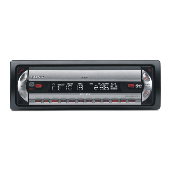
Photo: CDX-R3300
Model Name Using Similar Mechanism
CD Drive Mechanism Type
Optical Pick-up Name
SPECIFICATIONS
AM
Tuning range
Antenna terminal
Intermediate frequency 10.7 MHz/450 kHz
Sensitivity
Power amplifier section
Outputs
Speaker impedance
Maximum power output 52 W × 4 (at 4 ohms)
General
Outputs
Inputs
Tone controls
FM/AM COMPACT DISC PLAYER
US Model
Canadian Model
E Model
CDX-R3300/R3300S
NEW
MG-611MA-186//K
KSS1000E
US, Canadian Model:
530 – 1,710 kHz
E Model:
AM tuning interval:
9 kHz/10 kHz switchable
531 – 1,602 kHz (at 9 kHz step)
530 – 1,710 kHz (at 10 kHz step)
External antenna connector
30 µV
Speaker outputs
(sure seal connectors)
4 – 8 ohms
Audio outputs terminal (rear/sub switchable)
Power antenna relay control terminal
Power amplifier control terminal
Antenna input terminal
Remote controller input terminal (E Model)
Low: ±10 dB at 60 Hz (XPLOD)
Mid: ±10 dB at 1 kHz (XPLOD)
High: ±10 dB at 10 kHz (XPLOD)
– Continued on next page –
CDX-R3300
1
Advertisement
Table of Contents

Related Manuals for Sony CDX-R3300


Summary of Contents for Sony CDX-R3300
- Page 1 Mid: ±10 dB at 1 kHz (XPLOD) Frequency response 30 – 15,000 Hz High: ±10 dB at 10 kHz (XPLOD) – Continued on next page – FM/AM COMPACT DISC PLAYER Sony Corporation 9-961-431-01 2003L04-1 e Vehicle Company © 2003. 12 Published by Sony Engineering Corporation...
- Page 2 NE REMPLACER CES COMPOSANTS QUE PAR DES PIÈCES REPLACE THESE COMPONENTS WITH SONY PARTS WHOSE SONY DONT LES NUMÉROS SONT DONNÉS DANS CE MANUEL PART NUMBERS APPEAR AS SHOWN IN THIS MANUAL OR OU DANS LES SUPPLÉMENTS PUBLIÉS PAR SONY.
- Page 3 CDX-R3300/R3300S Notes on CD-Rs (recordable CDs)/CD-RWs (rewritable UNLEADED SOLDER CDs) Boards requiring use of unleaded solder are printed with the lead This unit can play the following discs: free mark (LF) indicating the solder contains no lead. (Caution: Some printed circuit boards may not come printed with the lead free mark due to their particular size.)
-
Page 4: Table Of Contents
CDX-R3300/R3300S TABLE OF CONTENTS 1. GENERAL Location of Controls (US, Canadian Model) ......5 Location of Controls (E Model) ..........5 Connections (US, Canadian Model) ........6 Connections (E Model) ............7 2. DISASSEMBLY 2-1. Sub Panel (1) Assy .............. 9 2-2. -
Page 5: General
CDX-R3300/R3300S SECTION 1 GENERAL This section is extracted from instruction manual. (US, Canadian Model) (E Model) -
Page 6: Connections (Us, Canadian Model)
CDX-R3300/R3300S Connections (US, Canadian Model) -
Page 7: Connections (E Model)
CDX-R3300/R3300S Connections (E Model) -
Page 8: Disassembly
CDX-R3300/R3300S SECTION 2 DISASSEMBLY Note : This set can be disassemble according to the following sequence. 2-1. SUB PANEL (1) ASSY (Page 9) 2-2. CD MECHANISM BLOCK (Page 9) 2-10. SERVO BOARD 2-3. MAIN BOARD 2-4. CHASSIS (T) SUB ASSY... -
Page 9: Sub Panel (1) Assy
CDX-R3300/R3300S Note : Follow the disassembly procedure in the numerical order given. 2-1. SUB PANEL (1) ASSY 3 two claws 2 two claws 1 two screws (+PTT 2.6 x 6) 4 sub panel (1) assy 2-2. CD MECHANISM BLOCK 7 bracket (CD) -
Page 10: Main Board
CDX-R3300/R3300S 2-3. MAIN BOARD 1 three screws (+BTT) 2 two screws (+PTT 2.6 x 8) 3 MAIN board 2-4. CHASSIS (T) SUB ASSY 4 claw 2 two screws (+P 1.7 x 2.2) 1 two screws (+P 1.7 x 2.2) 6 chassis (T) sub assy... -
Page 11: Roller Arm Assy
CDX-R3300/R3300S 2-5. ROLLER ARM ASSY 3 washer (1.1 – 2.5) 5 roller arm assy 4 worm wheel (RA) 2 spring (RAR) 1 spring (RAL) 2-6. CHASSIS (OP) ASSY qa chassis (OP) assy 0 compression spring (damper) lever (D) 4 washer... -
Page 12: Optical Pick-Up
CDX-R3300/R3300S 2-7. OPTICAL PICK-UP 2 chucking arm sub assy 5 claw 1 tension coil spring (CHKG) 7 optical pick-up 6 main shaft 4 rack (SL) 3 screw (+B 1.4 x 5) 2-8. SL MOTOR ASSY (M902) 1 screw (+P 1.4 x 1.8) -
Page 13: Le Motor Assy (M903)
CDX-R3300/R3300S 2-9. LE MOTOR ASSY (M903) 8 screw 0 woam (LEB) assy (+M 1.7 x 2.5) 9 bearing (LEB) 2 washer qa screw (+M 1.7 x 2.5) qf two toothed lock screws 3 gear (LE1) (+M 1.4 ) lever (D) -
Page 14: Diagrams
CDX-R3300/R3300S SECTION 3 DIAGRAMS 3-1. IC PIN DESCRIPTIONS • IC3 CXD3059AR (DIGITAL SERVO/DIGITAL SIGNAL PROCESSOR) (SERVO BOARD (1/2)) Pin No. Pin Name Pin Description MIRR Mirrer signal input/output DFCT Defect signal input/output Focus OK signal input/output — Ground pin LOCK Not used in this set. - Page 15 CDX-R3300/R3300S Pin No. Pin Name Pin Description CLTV VCO1 control voltage input FILO Filter signal output for master PLL FILI Filter signal input for master PLL Charge pump output for master PLL AVDD5 — Analog power supply pin DDVROUT DC/DC converter output...
- Page 16 CDX-R3300/R3300S Pin No. Pin Name Pin Description XLAT Latch signal input CLOK Serial data transfer clock signal input — Digital power supply pin for internal SENS SENS signal output SCLK Clock signal input for SENS serial data read out ATSK...
- Page 17 CDX-R3300/R3300S • IC801 MB90467PF-G-104-BNDE1 (SYSTEM CONTROL) (MAIN BOARD (2/2)) Pin No. Pin Name Pin Description Audio mute control signal output 2 to 4 — Not used in this set. (Open) BEEP Beep signal output to power amp IC VOL ATT...
- Page 18 CDX-R3300/R3300S Pin No. Pin Name Pin Description SYS RST System reset signal output TEL ATT TEL ATT signal output Not used in this set. (Open) ACC IN Accessory power supply detect signal input SIRCS Remote control signal (infrared rays) input RAM BU Not used in this set.
-
Page 19: Block Diagram -Cd Section
CDX-R3300/R3300S 3-2. BLOCK DIAGRAM — CD SECTION — • R-ch is omitted due to same as L-ch. • Siganal Path : CD PLAY DETECTOR MAIN RFACO 42 RFACI ASYO 45 ASYI AOUT1 CD-L SECTION (Page 20) AOUT2 R-CH RF AMP,DIGITAL SERVO,... -
Page 20: Block Diagram -Main Section
CDX-R3300/R3300S 3-3. BLOCK DIAGRAM — MAIN SECTION — ELECTRONIC VOLUME IC401 CD-L PJ401 9 C2 SECTION OUTS1 (Page 19) R-CH 8 C1 REAR OUTS2 R-CH AUDIO OUT R-CH POWER AMP MUTE TUX601 IC100 Q407 (TUNER UNIT) CNP901 PJ601 1 ANT... -
Page 21: Block Diagram -Display Section
CDX-R3300/R3300S 3-4. BLOCK DIAGRAM — DISPLAY SECTION — 3-5. CIRCUIT BOARDS LOCATION SYSTEM CONTROL LCD DRIVER SERVO board IC801 (3/3) IC501 SENSOR board KEYIN0 KEY MATRIX SPEAKER board S501-522 LCD501 LCD SO SEG3 KEYIN1 LCD SCK LIQUID SEG50 LCD CE... -
Page 22: Note For Printed Wiring Boards And Schematic Diagrams
CDX-R3300/R3300S 3-6. NOTE FOR PRINTED WIRING BOARDS AND SCHEMATIC DIAGRAMS 3-7. WAVEFORMS THIS NOTE IS COMMON FOR PRINTED WIRING — Servo Board — BOARDS AND SCHEMATIC DIAGRAMS. — Main Board — (MODE: CD PLAY) (In addition to this, the necessary note is printed in each block.) -
Page 23: Printed Wiring Boards -Cd Mechanism Section
CDX-R3300/R3300S 3-8. PRINTED WIRING BOARDS — CD MECHANISM SECTION — • Refer to page 21 for Circuit Boards Location. : Uses unleaded solder. R107 R139 R116 C110 R109 C109 R102 C115 R111 R144 R122 R128 R127 R143 R141 R119 R117... -
Page 24: Schematic Diagram -Cd Mechanism Section (1/2)
CDX-R3300/R3300S 3-9. SCHEMATIC DIAGRAM — CD MECHANISM SECTION (1/2) — • Refer to page 22 for Waveforms. TP59 TP60 TP57 TP61 TP180 TP181 TP129 TP72 TP123 TP128 TP139 TP53 TP56 TP140 TP55 TP167 TP54 TP48 TP49 TP71 TP175 TP47 R114... -
Page 25: Schematic Diagram -Cd Mechanism Section (2/2)
CDX-R3300/R3300S • Refer to page 22 for Waveforms. 3-10. SCHEMATIC DIAGRAM — CD MECHANISM SECTION (2/2) — • Refer to page 31 for IC Block Diagram. (Page 24) R136 R146 R117 TP70 IC B/D TP11 TP12 R140 TP19 TP20 TP17... -
Page 26: Schematic Diagram -Main Section (1/2)
CDX-R3300/R3300S 3-11. SCHEMATIC DIAGRAM — MAIN SECTION (1/2) — • Refer to page 32 for IC Block Diagram. TUX601 C600 PJ601 PJ401 C435 C436 JR10 C303 C108 IC100 IC B/D C113 C424 R416 C440 R431 Q405 R421 IC401 C101 Q404... -
Page 27: Schematic Diagram -Main Section (2/2)
CDX-R3300/R3300S 3-12. SCHEMATIC DIAGRAM — MAIN SECTION (2/2) — • Refer to page 22 for Waveforms. (Page 26) C447 R447 C802 R837 C809 D702 R821 R813 C801 R823 C446 C441 C810 R822 R448 D820 CN751 C709 D701 C707 R834 R832... -
Page 28: Printed Wiring Boards -Main Section
CDX-R3300/R3300S 3-13. PRINTED WIRING BOARDS — MAIN SECTION — • Refer to page 21 for Circuit Boards Location. : Uses unleaded solder. PJ401 PJ601 CNP900 CNP901 C435 C436 C303 C108 R442 C113 R427 R443 JW111 F901 R421 R418 IC100 C437... -
Page 29: Printed Wiring Board -Display Section
CDX-R3300/R3300S 3-14. PRINTED WIRING BOARD — DISPLAY SECTION — • Refer to page 21 for Circuit Boards Location. : Uses unleaded solder. S509 S513 S503 LED503 LED521 LED517 S516 S515 LCD501 S523 LED513 LED514 LED516 IC502 LED520 S502 S501 LED511... -
Page 30: Schematic Diagram -Display Section
CDX-R3300/R3300S 3-15. SCHEMATIC DIAGRAM — DISPLAY SECTION — R552 R551 R534 LED501 IC906 R571 R573 R575 R577 R579 LED503 R537 LED515 LED512 LED509 LED505 LED513 IC502 R533 R536 R532 CN901 LED502 R531 LED517 LED518 LED510 LED522 LED521 Q501 D521 IC501... -
Page 31: Ic Block Diagrams
CDX-R3300/R3300S 3-16. IC BLOCK DIAGRAMS IC1 LA6560-TE-L-E (SERVO Board) 36 S-GND THERMAL SHUTDOWN INPUT 35 VCONT BTL-AMP VCC2 MUTE 34 MUTE OUTPUT OUTPUT ON/OFF VLO- CONTROL 33 VIN4 VLO+ 32 VIN4- LEVEL 31 VIN4+ VO4+ SHIFT VO4- 30 VREF-IN LEVEL... - Page 32 CDX-R3300/R3300S IC7 R1114N151D-TR-FA (SERVO Board) 5 VOUT CURRENT VREF LIMIT IC401 BD3808FS (MAIN Board) FADER FADER FADER FADER (0~-58, (0~-58, (0~-58, (0~-58, C BUS -∞dB) -∞dB) -∞dB) -∞dB) GAIN+ATT LOGIC (+10~-29, -∞dB) 2ND ORDER LPF EFFECT (0dB~ EFFECT (0dB~ +20dB,2dB STEP)
-
Page 33: Exploded Views
CDX-R3300/R3300S SECTION 4 EXPLODED VIEWS NOTE: • The mechanical parts with no reference • Color Indication of Appearance Parts The components identified by mark 0 or dotted line with mark number in the exploded views are not supplied. Example : 0 are critical for safety. -
Page 34: Front Panel Section
CDX-R3300/R3300S 4-2. FRONT PANEL SECTION not supplied (DISPLAY board) not supplied LCD501 not supplied not supplied supplied not supplied Ref. No. Part No. Description Remark Ref. No. Part No. Description Remark X-3384-620-1 PANEL (BASE) ASSY, FRONT (R3300:US,CND) X-3378-390-3 CASE ASSY (for FRONT PANEL) -
Page 35: Cd Mechanism Section (1)
CDX-R3300/R3300S 4-3. CD MECHANISM SECTION (1) (MG-611MA-186//K) not supplied not supplied (SENSOR board) not supplied not supplied Ref. No. Part No. Description Remark Ref. No. Part No. Description Remark A-3372-455-A CHASSIS (T) SUB ASSY 3-253-748-01 DAMPER (S) 3-253-729-01 SPRING (LTR), TENSION COIL 3-352-758-31 SCREW (M1.7), TOOTHED LOCK... -
Page 36: Cd Mechanism Section (2)
CDX-R3300/R3300S 4-4. CD MECHANISM SECTION (2) (MG-611MA-186//K) (including M901) M902 not supplied not supplied not supplied not supplied The components identified by Les composants identifiés par une mark 0 or dotted line with mark marque 0 sont critiques pour 0 are critical for safety. -
Page 37: Cd Mechanism Section (3)
CDX-R3300/R3300S 4-5. CD MECHANISM SECTION (3) (MG-611MA-186//K) M903 Ref. No. Part No. Description Remark Ref. No. Part No. Description Remark 3-262-755-01 WASHER (1.1-2.5) 3-259-467-01 BRACKET (LEM) 3-259-024-01 WHEEL (RA), WORM 3-345-648-91 SCREW (M1.4), TOOTHED LOCK A-3337-633-A ARM ASSY, ROLLER A-3372-456-A WORM (LEB) ASSY... -
Page 38: Cd Mechanism Section (4)
CDX-R3300/R3300S 4-6. CD MECHANISM SECTION (4) (MG-611MA-186//K) Ref. No. Part No. Description Remark Ref. No. Part No. Description Remark 3-259-429-01 WHEEL (LE), WORM 3-899-829-01 WASHER (SLIT) 3-344-223-01 WASHER 3-259-032-01 GEAR (LE2) 3-259-470-01 GEAR (LE1) A-3372-453-A CHASSIS (M) BLOCK ASSY 3-253-755-01 LEVER (D) -
Page 39: Electrical Parts List
CDX-R3300/R3300S SECTION 5 DISPLAY ELECTRICAL PARTS LIST NOTE: • Due to standardization, replacements in • Items marked “*” are not stocked since The components identified by mark 0 or dotted line with mark the parts list may be different from the they are seldom required for routine service. - Page 40 CDX-R3300/R3300S DISPLAY MAIN Ref. No. Part No. Description Remark Ref. No. Part No. Description Remark R537 1-216-813-11 METAL CHIP 1/10W < CAPACITOR > R551 1-216-825-11 METAL CHIP 2.2K 1/10W R552 1-216-815-11 METAL CHIP 1/10W C101 1-124-233-11 ELECT 10uF R553 1-216-821-11 METAL CHIP...
- Page 41 CDX-R3300/R3300S MAIN Ref. No. Part No. Description Remark Ref. No. Part No. Description Remark C823 1-162-927-11 CERAMIC CHIP 100PF < JUMPER RESISTOR > C824 1-162-927-11 CERAMIC CHIP 100PF C825 1-124-584-00 ELECT 100uF 1-216-864-11 METAL CHIP 1/10W C908 1-126-960-11 ELECT 1-216-864-11 METAL CHIP...
- Page 42 CDX-R3300/R3300S MAIN SENSOR SERVO Ref. No. Part No. Description Remark Ref. No. Part No. Description Remark R435 1-216-809-11 METAL CHIP 1/10W R861 1-216-809-11 METAL CHIP 1/10W R436 1-216-809-11 METAL CHIP 1/10W R437 1-216-821-11 METAL CHIP 1/10W R862 1-216-809-11 METAL CHIP...
- Page 43 CDX-R3300/R3300S SERVO Ref. No. Part No. Description Remark Ref. No. Part No. Description Remark 1-107-826-11 CERAMIC CHIP 0.1uF C115 1-162-966-11 CERAMIC CHIP 0.0022uF 10% 1-164-227-11 CERAMIC CHIP 0.022uF 1-164-227-11 CERAMIC CHIP 0.022uF < CONNECTOR > 1-107-826-11 CERAMIC CHIP 0.1uF 1-162-962-11 CERAMIC CHIP...
- Page 44 CDX-R3300/R3300S SERVO Ref. No. Part No. Description Remark Ref. No. Part No. Description Remark 1-218-990-11 SHORT CHIP R119 1-218-941-81 RES-CHIP 1/16W 1-218-985-11 RES-CHIP 470K 1/16W R122 1-218-941-81 RES-CHIP 1/16W 1-218-965-11 RES-CHIP 1/16W R123 1-218-990-11 SHORT CHIP 1-218-977-11 RES-CHIP 100K 1/16W...
- Page 45 CDX-R3300/R3300S Ref. No. Part No. Description Remark PARTS FOR INSTALLATION AND CONNECTIONS *************************************** X-3382-647-1 FRAME ASSY, FITTING X-3366-405-1 SCREW ASSY (EXP), FITTING (E) 3-934-325-01 SCREW (+K 5X8 TP) 3-260-282-01 COLLAR 3-246-471-01 KEY (FRAME) 1-776-206-21 CORD (WITH CONNECTOR) (POWER)
- Page 46 CDX-R3300/R3300S REVISION HISTORY Clicking the version allows you to jump to the revised page. Also, clicking the version at the upper on the revised page allows you to jump to the next revised page. Ver. Date Description of Revision 2003. 12...