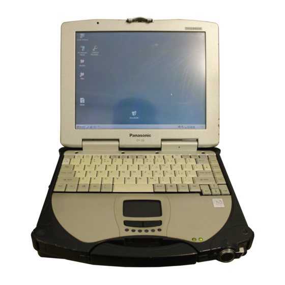
Panasonic Toughbook CF-28 Service Manual
Notebook computer
Hide thumbs
Also See for Toughbook CF-28:
- Reference manual (72 pages) ,
- Operating instructions manual (37 pages) ,
- Simplified service manual (14 pages)
Table of Contents
Advertisement
When this product is repaired, the Access Key is necessary
to release security of electrical and mechanical.
Ask the customer to provide the Access Key with this product.
Model Number Reference
The models in the CF-28 series are numbered in accordance with the types of the CPU, LCD
and HDD etc. featured by the product.
Model No.CF-28
CPU type
®
M: for Intel
Mobile Pentium
Processor 600 MHz
LCD type
C: for 13.3" TFT Color
with Touch Screen
HDD type / RAM size
F: 20 GB / 128 MB
This service information is designed for experienced repair technicians only and is not designed for use by the general public. It does not contain
warnings or cautions to advise non-technical individuals of potential dangers in attempting to service a product. Products powered by electricity
should be serviced or repaired only by experienced professional technicians. Any attempt to service or repair the product or products dealt with in
this service information by anyone else could result in serious injury or death.
Z
®
III
WARNING
ORDER NO. CPD0102001C0
Notebook Computer
CF-28
This is the Service Manual for
the following areas.
M ...for U.S.A. and Canada
E ...for U.K.
G ...for Germany
F ...for France
S ...for Sweden
T ...for Italy
P ...for Spain
Area
M: for U.S.A. and Canada
E: for U.K.
G: for Germany
F: for France
S: for Sweden
T: for Italy
P: for Spain
Operating System
®
C: Microsoft
Windows NT
®
®
D: Microsoft
Windows
®
®
E: Microsoft
Windows
Drive
A: Floppy Disk drive
© 2001 Matsushita Electric Industrial Co., Ltd.
All rights reserved. Unauthorized copying and
distribution is a violation of law.
®
2000
98
Advertisement
Table of Contents

Related Manuals for Panasonic Toughbook CF-28


Summary of Contents for Panasonic Toughbook CF-28
-
Page 1: Notebook Computer
Ask the customer to provide the Access Key with this product. Model Number Reference The models in the CF-28 series are numbered in accordance with the types of the CPU, LCD and HDD etc. featured by the product. Model No.CF-28... - Page 2 - 2 -...
-
Page 3: Lithium Battery
LITHIUM BATTERY CAUTION Danger of explosion if battery is incorrectly replaced. Replace only with the same or equivalent type recommended by the equipment manufacture. Discard used batteries according to the manufacturer's instructions. LITHIUMBATTERIES Vorsicht! Explosionsgefahr bei unsachgemäßem Austausch der Batterie. Ersatz nur durch denselben order einen vom Hersteller empfohlenen ähnlichen Typ. -
Page 4: Table Of Contents
Contents 1. Specifications 1-1, 1-2 ............2. Name and Functions of Parts 2-1, 2-2 ......3. Technical information 3-1~3-4 ........3.1. System Overview..........3-1, 3-2 3.2. System Memory Map........3.3. I/O Address Map..........4. Diagnosis Procedure 4-1~4-12 .......... 4.1. Basic Procedures..........4.2. -
Page 5: Specifications
Check the bottom of the computer or the box the computer came in at the time of purchase. To check CPU speed: Use DMI Viewer in [Start] - [Programs] - [Panasonic] - [DMI Viewer]. To check memory size and hard disk drive (HDD) size: 1 Run the Setup Utility. - Page 6 Touch Pad, Touchscreen (Anti-Reflection, Finger and stylus (included) touch capable) Internal Microphone Monaural Microphone (built in) Speaker Monaural Speaker (built in) Utility Programs Setup Utility, DMI Viewer, Panasonic Hand Writing* Sound , 44.1 PCM/FM Sound Battery Battery Pack Li-ion 11.1 , 5.4 Operating Time* Approx.
-
Page 7: Names And Functions Of Parts
2. Names and Functions of Parts LED Indicators Function Keys Internal Microphone Touch Pad DC-IN Jack Infrared Communication Port PC Card Slots Access Lock Internal Modem Power Switch Speaker Fn + F5 Speaker on/off : Fn + F4 Security Lock LOCK Carrying Handle LED Indicators... - Page 8 Microphone Jack External Display Port Parallel Port Serial Port Expansion Bus Connector External Keyboard/Mouse Port Headphone Jack USB Port MP Release Lever Battery Pack Hard Disk Drive Attaching the strap 2 - 2...
-
Page 9: Technical Information
3. Technical Information 3.1. System Overview 3.1.1 System Configuration The main system is made up of a Main board, a RJ board, an IR board, a Battery board and a TS13 board. The CPU operates at 1.6V, 1.35V(core)/2.5V; the main memory at 3.3V; the core logic at 3.3V/5V; and the other main chips at 3.3V. - Page 10 System Congiguration Diagram i i i i n n n n t t t t l l l l e e e e M M M M o o o o b b b b i i i i l l l l e e e e P P P P e e e e n n n n t t t t i i i i u u u u m m m m 1.5V GTL 64bit Host Bus...
-
Page 11: System Memory Map
3.2. System Memory Map 3 - 3... -
Page 12: I/O Address Map
3.3. I/O Address Map Address Function IC No. x0000 - x000F Direct memory access controller x0010 - x0018 Motherboard resources x001F - x001F Motherboard resources x0020 - x0021 Programmable interrupt controller x0022 - x0022 Motherboard resources x0024 - x0025 Motherboard resources x0028 - x0029 Motherboard resources x002C - x002D... -
Page 13: Diagnosis Procedure
4. Diagnosis Procedure 4.1. Basic Procedure The basic procedures for diagnosis, disassembly, and test of defective parts of a set to be repaired are summarized below. .or details, refer to relevant pages in the Service Manual. l l l l l .low Chart OCCURRENCE OF TROUBLE Power sw is set to ON. -
Page 14: Power-On Self Test (Boot Check)
4.2. Power-On Self Test (Boot Check) 4.2.1 Outline of POST The set has a boot check function called POST (Power-On Self Test) in it. The condition of the main body is diagnosed by checking beep sound or error code. l Start .....Test begins automatically when power switch is set to ON. l Normal finish ..After memory checking, a beep sound is issued once and the set is placed into automatic stop. -
Page 15: List Of Error Codes
If your system displays one of except the messages marked below with an asterisk (*), write down the message and contact Panasonic Technical Support. If your system fails after you make changes in the Setup menus, reset the computer, enter Setup and install Setup defaults or correct the error. - Page 16 02F0: CPU ID: CPU socket number for Multi-Processor error. 02F4: EISA CMOS not writable ServerBIOS2 test error: Cannot write to EISA CMOS. 02F5: DMA Test Failed ServerBIOS2 test error: Cannot write to extended DMA (Direct Memory Access) registers. 02F6: Software NMI Failed ServerBIOS2 test error: Cannot generate software NMI (Non-Maskable Interrupt).
-
Page 17: Diagnosis Map
4.4. Diagnosis Map 4.4.1 MAIN UNIT DIAGNOSIS (1/2) Make sure that connecting cables, connectors and AC adapter are not loose or disconnected prior to testing. Troubleshooting Source of Symptom Component procedures problem Result No power is sent to the Is 15V applied to pins 5-8 of YES Go to No. - Page 18 Troubleshooting Source of Symptom Component procedures problem Result No Sound Software setting Check software setting. Volume does not work. Go to No. 4-2 Replace the Speakers. Speakers Does operation return to Go to No. 4-3 normal? IC50 Replace the Main PCB. Main PCB IC51 Default configuration in...
- Page 19 4.4.3 LCD DIAGNOSIS Make sure that connecting cables, connectors and AC adapter are not loose or disconnected prior to testing. Troubleshooting Source of Symptom Component procedures problem Result No picture appears on the Does the LCD display Brigntness screen. properly after brightness adjustment level is adjusted? Go to No.
- Page 20 4.4.4 KEYBOARD, MOUSE or TOUCH PAD DIAGNOSIS Make sure that connecting cables, connectors and AC adapter are not loose or disconnected prior to testing. Troubleshooting Source of Symptom Component procedures problem Result Key top cannot be pressed. Keyboard is broken. Keyboard Key top does not spring back after pressing.
- Page 21 4.4.5 FDD DIAGNOSIS Make sure that connecting cables, connectors and AC adapter are not loose or disconnected prior to testing. Troubleshooting Source of Symptom Component procedures problem Result Access lamp does not Replace the FDD. light. Does operation return to Go to No.
- Page 22 4.4.6 HDD DIAGNOSIS Make sure that connecting cables, connectors and AC adapter are not loose or disconnected prior to testing. Troubleshooting Source of Symptom Component procedures problem Result Does not boot from HDD. Go to No. 1-2 Has the HDD been partitioned? Improper setting Go to No.
- Page 23 Troubleshooting Source of Symptom Component procedures problem Result An operating system could Format data Does executing FDISK not be found destroyed correct the problem? Go to No. 8-2 Replace the HDD. Does operation return to Go to No. 8-3 normal? Replace the HDD cable.
- Page 24 4.4.8 PRINTING DIAGNOSIS Make sure that connecting cables, connectors and AC adapter are not loose or disconnected prior to testing. Troubleshooting Source of Symptom Component procedures problem Result Data does not print from YES Main PCB IC47 Does the printer pass its the printer.
-
Page 25: Diagnostic Test
5. Diagnostic Test 5.1. Diagnostic Test Procedure 5.1.1 Equipment (1) Test Computer ............................1 unit (2) AC Adapter ............................1 pc. (3) External Printer ............................. 1 unit (4) Loopback Plug (Parallel Port Test) [P/N: D.WV95C0081] ..............1 pc. (5) Loopback Plug (Serial Port Test for RS232C) [P/N: D.WV95C0067] ..........1 pc. (6) .loppy Disk containg file DIAG ...................... -
Page 26: Test Procedure
5.1.4 Test Procedure Use the floppy disk containing file diag28. Press [D] [I] [A] [G] [2] [8] and [Enter] keys. DIAGNOSTIC MENU (V*.*L**) 1. TEST ALL DEVICES DEVICES) 2. TEST AUTOMATICALLY ( DEVICES) 3. EXIT 4. MAIN BOARD 5. xxxxxKB RANDOM ACCESS MEMORY 6. - Page 27 3) KEYBOARD TEST Press 6 and Enter keys. KEYBOARD 1. TEST ALL DEVICES DEVICES) 2. TEST AUTOMATICALLY ( DEVICES) 3. EXIT 4. PRESS KEY TEST 5. SCAN CODE RETURN TEST SELECT MENU : _ .or 4. PRESS KEY TEST. Press 4 and Enter Keys. PRESS KEY TEST 1.
- Page 28 5) BATTERY PACK TEST Press 8 and Enter keys. BATTERY PACK TEST Battery Pack : exists. AC Adaptor : connected (Not connected) (Normal message) : Test done ! ! Press any key when ready._ When an error message is displayed, refer to [5.2 Error Massage]. 6) VIDEO TEST Press 9 and Enter keys.
- Page 29 .or 4. HDD - DRIVE TEST. Press 4 and Enter keys. 1st HDD - DRIVE TEST Count value to get SEEK COMPLETE = 0 (Normal Message) : Test done ! ! Press any key when ready._ When an error message is displayed, refer to [5.2 Error Message] .or 5.
- Page 30 .or 5. 1st .LOPPY DISK DRIVE TEST. Press 5 and Enter keys. 1st .LOPPY DISK DRIVE TEST 1. TEST ALL DEVICES DEVICES) 2. TEST AUTOMATICALLY ( DEVICES) 3. EXIT 4. DRIVE TEST 5. 720KB - MEDIA TEST 6. 1.44MB - MEDIA TEST SELECT MENU : _ .or 4.
- Page 31 .or 4. PRINT OUT TEST. Press 4 and Enter keys. 1st Parallel port test (I/O address xxxH) Connect printer Hit any key when ready._ (Normal Message): Sample characters will be printed to the printer. 1st Parallel port test (I/O address 378H) !"#$%&'()*+,-./0123456789:;<=>?@ABCDEFGHIJKLMNOPQRSTUVWXYZ[\]ˆ_`abcdefghijklmno !"#$%&'()*+,-./0123456789:;<=>?@ABCDEFGHIJKLMNOPQRSTUVWXYZ[\]ˆ_`abcdefghijklmnop "#$%&'()*+,-./0123456789:;<=>?@ABCDEFGHIJKLMNOPQRSTUVWXYZ[\]ˆ_`abcdefghijklmnopq...
- Page 32 .or 4. RS232C CONTROLLER REGISTER R/W TEST. Press 4 and Enter keys. 1st serial port test (I/O address xxxH) (Normal Message): Test done ! ! Press any key when ready._ When an error message is displayed, refer to [5.2 Error Message]. .or 5.
- Page 33 .or 4. CONTROLLER REGISTER R/W TEST. Press 4 and Enter keys. CONTROLLER REGISTER R/W TEST Infrared port (I/O address xxxxH) (Normal Message): Test done ! ! Press any key when ready._ When an error message is displayed, refer to [5.2 Error Message]. .or 5.
-
Page 34: Error Message
5.2. Error Message IC43 IC43 IC43 IC43 IC79 IC43 IC43 IC35,IC37, IC39,IC41, IC80~IC83 IC35,IC37, IC39,IC41, IC80~IC83 IC35,IC37, IC39,IC41, IC80~IC83 IC1,IC33 5 - 10... - Page 35 IC43,IC79 IC79 IC47 5-14 IC47 5-14 IC47 5-14 5-14 5-14 5-14 5-14 5 - 11...
- Page 36 IC47 5-14 IC47 5-14 5-14 5-14 IC47 IC48 5-14 5-14 5-14 IC47 5-15 IC47 5 - 12...
- Page 37 IC47 IC50 IC20 5 - 13...
- Page 38 5 - 14...
- Page 39 5 - 15...
-
Page 40: Disassembly/Reassembly
Disassembly/Reassembly Note : Power off the computer. Do not shut down to the Suspend or hibernation mode. Do not add peripherals while the computer is in the Suspend or hibernation mode; abnormal operation may result. The Access Key is necessary to release security of electrical and mechanical. Ask the customer to provide the Access Key with this product. -
Page 41: Removing The Unit From Inside The Multimedia Pocket
6.3. Removing the Unit from 6.4. Removing the Keyboard inside the Multimedia Pocket <B> <A> Cover Cover Figure 7 1. Turn the main body upside down and open the Figure 10 Multimedia Pocket cover. 1. Open the connector cover at the rear of the main body and remove the two screws <A>. -
Page 42: Removing The Display Unit
6.5. Removing the Display Unit 6.7. Removing the Lower Casing and the Handle <D> Display Unit <F> Figure 14 1. Open the connector cover at the rear of the main Figure 12 body and remove the single screw <F>. 1. Disconnect the two connectors, CN9 and CN6, which Screw <F>... -
Page 43: Removing The Modem Board
6.8. Removing the I/O Board 6.10. Removing the MP Connection Unit <I> <H> CN706 IO Board <H> <K> <K> CN24 CN20 CN10 Connector A Figure 17 Connection Unit 1. Remove the three connectors, CN706, CN10 and Figure 19 CN20, to allow the I/O board to be separated from the main PCB. -
Page 44: Removing The Touch Pad Unit
6.12. Removing the Touch Pad 6.14. Removing RTC Battery Unit RTC Battery <M> Touch Pad Unit Figure 23 1. Remove the connector CN4, which connects RTC Figure 21 battery to the main PCB. Remove the four screws <M> that secure the touch pad 2. -
Page 45: Removing The Inverter, The Touch Screen Pcb And Ts13 Pcb
6.15. Removing the INVERTER, 6.16. Removing the LCD and the the Touch Screen PCB and Touch Screen TS13 PCB <P> <O> <O> Connector B Hold Plate FPC of <P> TOUCH SCREEN CN850 LATCH REAR Hold CABINET Back Damper Plate <O> Cable of <O>... -
Page 46: Wiring Connection Diagram
7. Wiring Connection Diagram PORT REPLICATOR PARALLEL SERIAL CN703 CN705 CN702 CN704 CN706 I/O PCB CN701 CN700 INVERTER BACKLIGHT Battery TS13 TOUCH SCREEN Phone PS/2 Jack Jack CN11 TOUCH SCREEN DC-IN CN23 CN10 CN20 CN14 KEYBOARD Connection Unit MAIN TESTER MODEM Jack JK800... -
Page 47: Exploded Views
8. Exploded Views K316 K133 K124 K124 K312 K316 K303 K210 K311 K130 K206 K304 K305 K313 E32-02 K311 K316 K131 K310 E32-01 K316 K123 K314 K123 K315 K140 K212 K205 K307 K304 K313 K142 K127 K301 E10-01 K204 K132 K302 E32-03 K306... - Page 48 BOTTOM CABINET TOP CABINET Screw tightening torque A 0.19 ± 0.02 N·m (2.0 ± 0.2 kgf·cm) E 0.49 ± 0.05 N·m (5.0 ± 0.5 kgf·cm) H 0.89 ± 0.05 N·m (9.0 ± 0.5 kgf·cm) I 0.10 ± 0.02 N·m (1.0 ± 0.2 kgf·cm) K150 K152 K149...
- Page 49 Screw tightening torque K 0.55 ± 0.051 N·m (5.5 ± 0.5 kgf·cm) K119 K118 K119 K115 K102 K107 K117 K105 K108 K110 K112 K100 K108 K116 K106 K101 K109 K108 K117 K114 K100 K105 K111 K107 K104 K101 K113 K402 K403 K401 K122...
-
Page 50: Replacement Parts List
9. Replacement Parts List (Main Block Unit, Mechanical Parts, Accessories and Packing Materrial) Note : Important Safety Notice Components identified by mark have special characteristics important for safety. When replacing any of these components, use only manufacturer's specified parts. REF. NO and Area PART NO DESCRIPTION Q'TY... - Page 51 REF. NO and Area PART NO DESCRIPTION Q'TY PACKING MATERIAL DFPE0611ZA HOLDER, MANUAL DFPK1063ZA CASE DFPN0754ZA CUSHION, PACKAGE MECHANICAL K201 DFHE5025XA SCREW K202 DFHG1415ZA DAMPER(A), HDD K203 DFHG1462ZA TAB(A), HDD K204 DFHM0229ZA SHAFT, HDD CONNECTOR K205 DFHR5851ZA CONNECTOR GUIDE, HDD K206 DFHR7960YB DAMPER(B), HDD...
- Page 52 REF. NO and Area PART NO DESCRIPTION Q'TY DFHG1465ZA PACKING, WATERPROOF, BODY DFHG1466ZA O-RING, LOCK LEVER DFHG1467ZA CUSHION, LEAD SWITCH DFHG808ZB CUSHION A, BATTERY DFHR7985ZA CUSHION B, BATTERY DFHG809ZA RUBBER, LCD STOP DFHG812ZA PACKING, WATERPROOF, KEYBOARD DFHG813ZA PACKING, WATERPROOF, LCD DFHG814ZB PACKINGRING, WATERPROOF, POWER SW DFHG815YA...
- Page 53 REF. NO and Area PART NO DESCRIPTION Q'TY XYN26+J5FZ SCREW XYN3+J10FN SCREW DFHE5092ZA SCREW(M3.0) DFGB0087ZA-0 BADGE, TOUGH BOOK DFHG1426YB DAMPER, LCD BACK DFKF8134YA-0 BOTTOM CABINET DFKM8140YA-0 TOP CABINET DFKM8141ZA-1 REAR CABINET, LCD DFBH1117ZA HINGE L DFBH1118ZA HINGE R DFBS9002ZA-0 LCD LATCH DFGB0070ZA-1 BADGE, PANA DFHG1319ZA...
- Page 54 REF. NO and Area PART NO DESCRIPTION Q'TY K146 DFMC0683ZA GASKET K147 DFHR7986ZA MICROPHONE SPACER K148 DFHR7981ZA MP GUIDE SPACER A K149 DFHR7982ZA MP GUIDE SPACER B K150 DFMD7778ZA MP GUIDE ANGLE K151 DFHR7978ZA SPACER R K152 DFKE0625ZB-0 REINFORCEMENT PART K153 DFMC0613ZA CONDUCTIVE CLOTH...
- Page 55 REF. NO and Area PART NO DESCRIPTION Q'TY C140, 141 DCUM1H180JCL CAPACITOR C150, 260, 261, 262, 263, 383, 397, ECUV1C105ZFX CAPACITOR, 16V, 1 µ F 416, 423 C168, 325, 326, 327, 363, 365, 366, EEFCD0J470R CAPACITOR, 2V, 47 µ F 367, 386, 387, 388, 403, 404, 405 C169, 268 DCUE1A106ZFL...
- Page 56 REF. NO and Area PART NO DESCRIPTION Q'TY IC34 DA9716CTBX3A IC, PLL IC35, 37, 39, 41, 80, 81, 82, 83 C3ABQG000025 IC, SDRAM IC43 DAFW82371M-I IC, PIIX4 IC45, 101, 104, 107, 117, 119, 124, DA7SH08U85L0 IC, AND GATE 125, 133, 134 IC46 DA2563A1SX2V IC, REGULATOR...
- Page 57 REF. NO and Area PART NO DESCRIPTION Q'TY Q1, 7 DA3LN01STL TRANSISTOR Q2, 8, 11, 12, 14, 16, 20, 21, 23, 35, DETC114YETL TRANSISTOR 36, 41, 55, 60, 64, 65, 66, 69, 73, 74 Q3, 62, 63 2SK3019TL TRANSISTOR DAFDS6690A TRANSISTOR Q5, 6 DAFDS6670A...
- Page 58 REF. NO and Area PART NO DESCRIPTION Q'TY R100 ERJ3GEYJ106V RESISTOR, 1/16W, 10MΩ R101 ERJ3GEYJ154V RESISTOR, 1/16W, 150kΩ R103, 178, 179, 185, 186, 187, 188, 200, 201, 202, 255, 265, 324, 348, ERJ3GEYJ473V RESISTOR, 1/16W, 47KΩ 422, 455, 472, 473, 487, 491, 500, R113, 114, 115, 116 ERJ3GEYJ270V RESISTOR, 1/16W, 27Ω...
- Page 59 REF. NO and Area PART NO DESCRIPTION Q'TY BATTERY PCB CN900 K1KB08A00075 CONNECTOR CN901 K1KB30A00105 CONNECTOR IR PCB C770, 771 DCUM1C104ZFK CAPACITOR C772 DCUJ1A105ZFL CAPACITOR, 10V, 1 µ F CAPACITOR, 2V, 47 µ F C773 EEFCD0J470R C774 ECUV1C224ZFV CAPACITOR, 16V, 0.22 µ F CN770 DFJS365ZA010 CONNECTOR...
- Page 60 CF-28 Printed Circuit Board MAIN PCB<Top View>...
- Page 61 Printed Circuit Board MAIN PCB<Bottom View>...
- Page 62 Printed Circuit Board Battery PCB FDD PCB I/O PCB IR PCB RJ PCB TS13 PCB...
- Page 63 CF-28MK2 Schematic Diagrams Main 1 CPU (1 / 2)
- Page 64 Main 2 CPU (2 / 2)
- Page 65 Main 3 GMCH3 (1 / 3)
- Page 66 Main 4 GMCH3 (2 / 3)
- Page 67 Main 5 GMCH3 (3 / 3)
- Page 68 Main 6 Clock...
- Page 69 Main 7 On Board Memory...
- Page 70 Main 8 SO DIMM...
- Page 71 Main 9 ICH3, USB (1 / 2)
- Page 72 Main 10 ICH3, USB (2 / 2)
- Page 73 Main 11 HDD I/F...
- Page 74 Main 12 MP, Tester CN...
- Page 75 Main 13 VCH...
- Page 76 Main 14 LCD I/F, Resister...
- Page 77 Main 15 PCIC-2Slot...
- Page 78 Main 16 PCMCIA-CN 2Slot...
- Page 79 Main 17 Super-I/O-1, Comsel GA...
- Page 80 Main 18 S-I/0-2, IRDA, BUF...
- Page 81 Main 19 KBC, KB Pad CN...
- Page 82 Main 20 Sound IC...
- Page 83 Main 21 Soundamp, Mic SPK...
- Page 84 Main 22 Ext CN...
- Page 85 Main 23 LED...
- Page 86 Main 24 Mini PCI...
- Page 87 Main 25 Bios, Resistor...
- Page 88 Main 26 PCIC 1Slot(1394)
- Page 89 Main 27 PCMCIA 1Slot...
- Page 90 Main 28 PME&KBC, LID...
- Page 91 Main 29 Hot Swap...
- Page 92 Main 30 Wireless module CN...
- Page 93 Main 31 VC1...
- Page 94 Main 32 VCT...
- Page 95 Main 33 VA18, VC15...
- Page 96 Main 34 VA3, VA5...
- Page 97 Main 35 VC3, VB3, VC5, VB5, Reset...
- Page 98 Main 36 DC-IN VM1 P-SW...
- Page 99 Main 37 Charger...
- Page 100 Main 38 2nd BAT CTL...
- Page 101 Main 39 SMI...
- Page 102 Main 40 LVDS...
- Page 103 I/O 1 CN...
- Page 104 I/O 2 CN...
- Page 105 I/O 3 CN...
- Page 106 CF-28MK2 Printed Circuit Board MAIN PCB<Top View>...
- Page 107 Printed Circuit Board MAIN PCB<Bottom View>...
- Page 108 Printed Circuit Board Battery PCB FDD PCB I/O PCB IR PCB RJ PCB TS13 PCB...
- Page 109 CF-28 Schematic Diagrams Main 1 CPU (1/2) HD#[0-63] HA#[3-31] Mobile Pentium III-600MHz Mobile Pentium III-600MHz 004:G1 004:J1 VCTREF HD#[63] R18 D63# HA#[3] VREF HD#[62] U18 D62# HA#[4] VC1=1.6V H10 VCC Icc= 12.6Amax(600MHz) VREF HD#[61] M19 D61# HA#[5] H12 VCC VREF...
- Page 110 Main 2 CPU (2/2) Mobile Pentium III-600MHz VC25 VCTREF CMOSREF 1.5K 0.5% 0.5% VCTREF=2/3VCT CMOSREF=1.0V RA77 0.1u 0.1u IERR# 001:C7 0.5% 0.5% A20M# 0.1u 0.1u 001:C9;009:F6 SLP# 001:C11 IGNNE# C516 001:C9;009:F6 0.1u PREQ# 001:C10;002:D10 C_INTR 001:C11;033:E10;033:F3 C_NMI 001:C11;033:E9;033:F3 FLUSH# 001:B11 1.5k C_STPCLK# VC25...
- Page 111 Main 3 VC1.6/1.35,VCT,VC25 1.6V 2125 1/4W 2125 1/4W ETQP6F1R3LFA 4.92m RB081L-20 2125 1/4W MACO MACO MACO MACO SPCAP SPCAP SPCAP SPCAP 3216 6.3V FDS6670A 2125 1/4W B C68 C515 100u 100u 100u 100u 2125 1/4W EEFCD0D101R EEFCD0D101R EEFCD0D101R EEFCD0D101R Nch-MOSFET R522 FAIRCHILD SOP8...
- Page 112 Main 4 CORE (1/2) 443BX IC33 HD#[0-63] HA#[3-31] 001:A1 443BX IC33 001:D1 MRAS3# MMRAS3# MMRAS0# AB14 CSA0#/RASA0# AE25 CSB0#/RASB0# 008:D6 TP65 HD#[0] HA#[3] B22 HD0# HA3# MRAS0# MMRAS0# MMRAS1# AF15 AD24 CSB1#/RASB1# CSA1#/RASA1# 007:A4;007:C4;007:E4;007:F4 TP66 HD#[1] HA#[4] D22 HD1# HA4# MCAS5# MMCAS5# MMRAS2#...
- Page 113 Main 5 CORE (2/2) 443BX IC33 G_AD[0-31] AD[0-31] 009:B1;015:C1;020:B2;024:B1;036:C1,009:B1;015:C1;020:B2;024:B1;036:C1,009:B1;015:C1;020:B2;024:B1;036:C1,009:B1;015:C1;020:B2;0 24:B1;036:C1,009:B1;015:C1;020:B2;024:B1;036:C1,009:B1;015:C1;020:B2;024:B1;036:C1,009:B1;015:C1;020 443BX IC33 AD[31] RA63 G_AD[31] G_AD31 AD31 G_FRAME# AD[30] 005:C6;013:B6 G_AD[30] G_AD30 AD30 G_IRDY# C500 C501 AD[29] 005:C6;013:B6 G_AD[29] G_AD29 AD29 G_TRDY# 6.3V 3216 6.3V 3216 6.3V 3216 AD[28] 6.3V 3216 6.3V 3216...
- Page 114 Main 6 CLOCK VC3CK DTC114YE SEL66M 004:B10;028:G4 SEL100/66# 006:C3 IC34 C105 IMIC9714ATB FCX-03-14.318Mhz HCLKCPU 14.318MHz CPUCLK0 24 XTAL_IN 001:A11 CPUCLK1 23 TP77 HCLKBX C113 004:I9 C106 H = 32mm ~ 34mm XTAL_OUT VC3CK SEL100/66# MA729 SEL100/66# 006:B2 A + H + 65mm <...
- Page 115 Main 7 ONBOARD MEMORY MA[0-13] MA[0-13] MA[0-13] MA[0-13] 004:C8;008:D3,004:C8;008:D4,004:C8;008:D4,004:C8;008 MD[0-63] 004:G2;008:D1 IC35 IC37 IC39 IC41 TC59SM716AFT-80 TC59SM716AFT-80 TC59SM716AFT-80 TC59SM716AFT-80 MA[11] MD[39] MA[11] MD[47] MA[11] MD[55] MA[11] MD[63] MD[38] MD[46] MD[54] MD[62] MA[12] MA[12] MA[12] MA[12] MD[37] MD[45] MD[53] MD[61] MA[13] MA[13] MA[13] MA[13]...
- Page 116 Main 8 EXT. MEMORY CON MD[0-63] SO-DIMM 54697-1443 SO-DIMM MD[0] MD[32] 54697-1443 MD[1] MD[33] MD[2] MD[34] MD[3] MD[35] MOLEX MD[4] MD[36] MD[5] MD[37] MD[6] MD[38] MD[7] MD[39] MCAS0# MCAS4# CE0# CE4# 004:B4;007:A5;007:A10 004:B3;007:A5;007:A10 MCAS1# MCAS5# CE1# CE5# 004:B2;007:C5;007:C10 004:B1;007:C5;007:C10 MA[0] MA[3] 004:C8;007:I1 004:C8;007:I1...
- Page 117 Main 9 PIIX4,USB (1/2) AD[0-31] PIIX4M IC43 PIIX4M IC43 PDD[0-15] AD[31] PDD[15] CDRST DACK0# U14 DACK0# AD31 LA23 PDD15 012:A5 017:B9;025:C6 AD[30] PDD[14] IRPSD# DACK1# W6 DACK1# AD30 LA22 PDD14 018:G7 017:B9;025:C6 AD[29] PDD[13] DISCOM_C DACK2# Y10 DACK2# AD29 LA21 PDD13 017:G7 017:B9;025:C7...
- Page 118 Main 10 PIIX4,USB (2/2) KB-ID PIIX4M IC43 ECSCI# INTMIC/PR# KBID1KBID0 GPI1 GPO0 010:F3;028:F2 021:G4 KBID0 DISCOM_D GPO8 T19 NC NC GPI13 US,UK 010:G2;019:B6 017:G7 KBID1 NOPCICD2# GPI14 GPO27 010:G2 036:A5 SHUT_COMB MPID0 GPI15 GPO28 010:H3;012:B7 PXCNF2 R476 022:B6 RA19 NOPCICD1# 010:C3 w/BL MPID1...
- Page 119 Main 11 HDD VC5HDM BLM21P600SG C164 C163 0.1u 6.3V 3216 VC5HDD VC5HDD C165 0.1u R122 RSTDRV DTC114YE 009:D8;017:B8;018:B5;019:I6 PDD[0-15] HDD CN R123 KX14050K11D-C75 PDD[7] PDD[8] PDD[6] PDD[9] PDD[5] PDD[10] PDD[4] PDD[11] PDD[3] PDD[12] PDD[2] PDD[13] PDD[1] PDD[14] PDD[0] PDD[15] PDIOW# 009:H4 PDIOR# PDDREQ...
- Page 120 Main 12 MP,TESTER CN VC5CDD SPCAP 6.3V C167 C168 0.1u 47uF EEFCD0J470R VC5CDD TSTVC5 SIORDY R131 RA72 SDDREQ 5.6K R130 MP I/F-1 MP I/F-2 VC5CDD FH12-40S-0.5SV FH12-40S-0.5SV SDD[7] 009:H4 SDD[15] 009:H4 TESTER_CN R136 R133 CN24 FH12-16S-0.5SV RA22 T_RTS1# VC5CDD 017:I4 T_DTR1# 017:D9;023:B6 017:I4...
- Page 121 Main 13 VGA SM710GX04A R(5) PDATA[21] SM710GX04A G_AD[0-31] 014:A3 :C1,005:C1,005:C1,005:C1 PDATA[20] R(4) PDATA47 M5 MD63 014:A3 005:A3;005:C9 PDATA[19] SM710GX04A R(3) MD62 MA10 PDATA46 014:A3 005:A3;005:C9 R(2) PDATA[18] MD61 PDATA45 014:A3 G_AD[31] AD31 PDATA35 005:A3;005:C9 AD_STBA AD_STB0 PDATA44 MD60 G_AD[30] 005:A3;005:C9 AD30 PDATA34 AD_STBB...
- Page 122 Main 14 LCD&CRT I/F,LVDS FPHDE IC73 013:E6 DAC63M63AX3H 013:E5 013:E5 ACB1608H-015 LVD2+ LVD2+ TO2+ LCD_CN2 014:I5 LVD2- LCD_CN1 LVD2- ACB1608H-015 TO2- 014:I5 PDATA[5] B(5) SM22B-SHLS-G-HB 013:D4 DF19G-20P-1H(59) PDATA[4] B(4) LVD1+ ACB1608H-015 LVD1+ 013:D4 TO1+ 014:I4 PDATA[3] B(3) LVD1- LVD1- ACB1608H-015 TO1- 013:D4 014:I4...
- Page 123 Main 15 PCMCIA CONT. AD[0-31] RB5C478II-BGA261 ACADR[0-25] RB5C478II-BGA261 AD[31] BCADR[0-25] ZV_HREF C11 VDHREF AD31 013:D10 AD[30] ACADR[25] BCADR[25] ZV_VSYNC B11 VDVS AD30 A_A25 B_A25 013:D10 AD[29] ZV_Y7 B14 VDY7 ACADR[24] BCADR[24] AD29 A_A24 B_A24 013:D9 AD[28] ZV_Y6 A15 VDY6 ACADR[23] BCADR[23] AD28 A_A23...
- Page 124 Main 16 PCMCIA I/F PCMCIA-2 PCMCIA-2 BCADR[0-25] ACADR[0-25] 62183-001 62183-001 BCDATA[0-15] ACDATA[0-15] PCMCIA-2 BCDATA[3] BCD1# ACDATA[3] ACD1# CD1# CD1# 015:G8;015:G10 015:G10;015:J8 62183-001 BCDATA[4] ACDATA[11] BCDATA[11] ACDATA[4] BCDATA[5] BCDATA[12] ACDATA[5] ACDATA[12] BCDATA[6] BCDATA[13] ACDATA[6] ACDATA[13] BCDATA[7] BCDATA[14] ACDATA[7] ACDATA[14] BCE1# BCDATA[15] ACE1# ACDATA[15] CE1#...
- Page 125 Main 17 SuperI/O-1,COMSEL GA IC72 uPD65882GC-041-8EU IC116 SA[15] 009:D2;017:B4;018:B2;025:E2;026:B2;032:F1 DCDA# DCD1# SA[14] DCDA DCD1 017:E6 017:F8;018:G3 009:D2;017:B4;018:B2;025:E2;026:B2;032:F1 IC116 DSRA# DSR1# DSRA DSR1 017:E6 TC74VHC32FT 017:F9;018:G3 SIN1 SINA SINA SIN1 IC116 017:E5 018:G3 SA[13] 009:D2;017:B4;018:B2;025:E2;026:B2;032:F1 RTSA# RTS1# TC74VHC32FT RTSA RTS1 017:E5 017:I9;018:G3 SA[12] SOUTA...
- Page 126 Main 18 SuperI/O-2,IrDA BUF CFG0=1:UART Mode BADDR :2E/2Fh IC48 MAX211ECAI-T R197 RID# VCC 11 017:G5 16V 2125 2125 DTRD# RI232C# 017:G5 022:E7;028:F3;032:C10 CTSD# V+ 13 C260 C262 017:G5 RTSD# DTC114YE 017:G5 IC49 SA[0-15] DCDD# V- 17 C264 017:G4 2125 16V 2125 PC97338VJG C263 SOUTD...
- Page 127 Main 19 KBC,K/B PAD CN DAP202U R216 R217 R218 R219 IC76 SN74CBT3306PW TSDATA5 014:G5 TSCLK5 014:G5 1OE# 4 GND CN53 IC79 2OE# FH12A-16S-1SH M38813M4-084HP C277 0.1u KB2_1 SCRLED# SSOP8 RA35 023:B4 KB2_2 NUMLED# P26 26 023:B3 KB2_3 CAPLED# P25 27 023:B2 KB2_4 PADLED#...
- Page 128 Main 20 SOUND IC IC144 MODEMAUDIO1 024:A8 CARDSPKR2 036:C8 TC7SH86FU R582 AD[0-31] IC147 IC50 ES1988S JP15 AD[31] VAUX 55 AD31 TC7SH86FU AD[30] VCCD 12 AD30 1608JP AD[29] VCCD 41 AD29 IC145 CARDSPKR1 AD[28] VCCD 90 015:E6 AD28 PIIXSPKR AD[27] 010:D2 AD27 C294 C297...
- Page 129 Main 21 Power Amp, MIC,SPK,H-PHONE VC5SA R252 VC5SA 6.3V R254 C317 3216 SNDGND1 R255 R245 C322 HSJ0942-01-1110 2.2K 0.1u R253 2.2K SNDGND1 IC111 BK1608HS601 TC7W66FU HOSHIDEN NJM2904M-TE1 I/O_1 O/I_1 C321 PRMIC R256 I/O_2 O/I_2 022:B7 020:G6 0.22u IC52 VC5SA BK1608HS601 IC122 IC112 INTMIC/PR#...
- Page 130 Main 22 Ext.IO I/F (FFC-CONN) LAN CN Port Reprecator I/F-1 CN20 FH12-40S-0.5SV PR_DCD1# 018:I3 TP220 PR_SIN1 018:I3 TP230 PR_SOUT1 TP222 018:I3 PR_DTR1# 018:I3 TP223 PR_DSR1# PR_DSR2# 018:I3 017:F9;017:I2 PR_RTS1# PR_RTS2# 018:I3 017:H9;017:I3 PR_CTS1# PR_CTS2# 018:I3 017:F9;017:I3 PR_RI1# PR_RI2# 018:I4 017:F10;017:I3 PRSTRB# PRPD7 017:E7...
- Page 131 Main 23 LED CAPLED# DTA114EE 019:F3 NUMLED# DTA114EE 019:F3 SCRLED# DTA114EE 019:F2 LEDzz RA36 SEC1703C CAPS LOCK PADLED# DTA114EE 019:F3 SEC1703C NUM LOCK SEC1703C SCROLL LOCK HDLED R124 011:F10 SEC1703C MP (FDD/CD-ROM/SUPER DISK) SEC1703C DTA114EE 012:D5;017:D9 R268 SEC1703C KEY PAD CDLED R269 012:A7...
- Page 132 Main 24 Mini PCI...
- Page 133 Main 25 Resistors SA[0-19] RA46 DRQ0 SA[17] 009:F2;017:B9 RA52 DRQ6 IRDY# 009:F3 SA[19] 005:D6;009:B6;015:C6;020:B7;024:B5;024:F5;036:C6 FRAME# SA[18] 005:D6;009:B6;015:C6;020:B6;024:D5;024:I5;036:C6 SERR# SA[16] 005:D7;009:B7;015:C7;024:B5;024:F6;036:C7 PLOCK# 005:D7 STOP# 005:D7;009:B7;015:C6;020:B7;024:D5;024:I5;036:C6 DRQ7 DEVSEL# RA45 009:F3 005:D6;009:B6;015:C6;020:B7;024:E6;024:I6;036:C6 DRQ5 TRDY# 009:F3 RA47 005:D6;009:B7;015:C6;020:B7;024:D5;024:I5;036:C6 SA[12] 005:D6;009:B6;015:C6;020:B6;024:E5;024:I5;036:C6 DRQ2 R290 SA[13] 009:F2;017:B9 DRQ3 R291 SA[14]...
- Page 134 Main 26 BIOS,VD12 BIOS SD[0-7] SA[0-18] SA[0-18] IC135 IC59 MBM29LV004TC SD[0-7] IC60 SA[17] SD[7] TC7S32FU SST39VF040-xxx-4C-WH SA[16] SD[6] SA[17] SD[7] SA[15] SD[5] SA[16] SD[6] SA[14] SD[4] SA[15] SD[5] SA[13] SD[3] SA[14] SD[4] SA[12] SD[2] IC135 ROMEN# SA[13] SD[3] SA[11] 032:H4 SD[1] IROMCS# SA[12]...
- Page 135 Main 27 VC3,VB3,VC5,VB5,Reset FDS6912A S1 1 G1 2 470K R323 R326 DTA144EE SPCAP S2 3 6.3V G2 4 C365 Nch-MOSFET 47uF C371 FAIRCHILD SOP8 EEFCD0J470R IC54 SUSB# DTC114YE IC113 PST9140 IC113 10k R537 220K R320 VOUT 4 VCRST# 001:D10;010:C3;026:D4;027:B11;028:E2;032:H4;033:D5 R317 NC 1 C368 560K...
- Page 136 Main 28 EC,LID IC20 CN14 HD64F3434TF16 BM02B-SRSS-TB LID# R354 AMBTHERM SUSC# PB0 91 SELFVPP 010:F3;028:J5 LID CN 009:F9;027:A4;027:C9 028:D11 VBRST# PB1 90 ECBTLW# 028:A4;028:H4 005:H8;015:E9;027:I5;036:E9 009:F7;010:F3 R329 VCRST# PB2 81 ECPWRSW# 001:D10;010:C3;026:D4;027:B11;027:I3;032:H4;033:D5 009:F8;010:F3 C384 PB3 80 ECLID# 028:I5 009:F8 VGASUS# PB4 69 ECRING# 013:A8...
- Page 137 Main 29 VA3,VA5 3.3V : R362=24.0k/R363=68.0k C394 C401 C390 1000p 1000p MAXIM SSOP28(1.99mmH) MAX1634CAI-T IC74 4.7u C395 6.3V 2125 C391 C400 0.1u 0.1u 2125 R360 C397 0.1u C399 C392 0.1u R357 2125 1/4W R366 2125 R355 1/4W R367 2125 1/4W 1/4W 2125 R356...
- Page 138 Main 30 DC-IN,VM1 PWR SW Main Battery Conn. CN17 AXK630235 CHARGE VMBATT SI4435DY SI4435DY 25V C410 0.1u Pch-MOSFET R379 R380 SOP8 TEMIC R381 ACVOK 2.2K 031:D5 2.2K 470K R382 2125 VC5SA 2125 Pch-MOSFET TEMIC SOP8 BATDTCT# R368 R369 028:B5;028:F2;030:C7 BATDATA R371 R370 028:H9;030:C8;035:F2...
- Page 139 Main 31 Charger BAT CN DC15 RB081L-20 R385 VMBATT 25V C412 0.1u C416 AC15 2125 1u SI4435DY RB715F R392 RB081L-20 1/4W 2125 3225 C418 Pch-MOSFET R393 R388 SOP8 TEMIC 1/4W 100K 2125 25V C417 R389 0.1u 100K CHARGE DTA144EE R383 R394 1/4W 5.6K...
- Page 140 Main 32 Wireless Module CONN. EXT_ROM R239 2125 SA[0-17] SD[0-7] 017:B4;018:B2;025:E2;026:B2,009:D2;017:B2;017:B4;018:B2;025:E2;026:B2,009:D2;017:B1;017:B4;018:B2;025:E2;026:B2,009:D2;017:B1;017:B4;018:B2;025:E2;026:B2,009:D2;017:B1;017:B4;018:B2;025:E2;026:B2,009:D2;025:E2;026:B2,009:D2;025:E2;026:B2 009:D4;017:B7;018:B4;019:D5;025:E6;026:I1;028:D6 SNDGND4 R240 EXTROM CN Config.-CN(A) 2125 CN19 CN18 SNDGND4 AXK660345P FH12-50S-0.5SH ---------------------------- SA[0] SD[0] SNDGND4 M_MICIN 020:E7;024:A8;024:F8 SA[1] SD[1] ---------------------------- SA[2] SD[2] PHONE3 020:G5 SA[3] SD[3] ---------------------------- SA[4] SD[4] SA[5] SD[5]...
- Page 141 Main 33 GCL R414 G_CPURST# CRESET# R411 004:I8 033:D6 R422 IC78 R423 UPD65837GA-Y15-9EU P_NMI C_NMI G_NMI 009:F7;033:C9 001:C11;002:I3;033:E9 P_INTR C_INTR G_INTR INTR 009:B8;033:C10 001:C11;002:I3;033:E10 P_INIT# C_INIT# INIT# G_INIT# 009:F6;033:C10 001:B11;002:I4;033:E10 JP18 A20M# G_A20M TP183 JP19 IGNNE# G_IGNNE# TP184 P_SMI# C_SMI# SMI# G_SMI# 009:F7;033:C11...
- Page 142 Main 34 Smart Card I/F Smart Card I/F CN13 FH12-10S-0.5SV SC_DSR# 017:I7 SC_SIN 017:I7;032:C11 SC_RI# 017:I7 SC_DTR# 017:I7 SC_SOUT 017:I7;032:C11 SC_IN# 035:F9 HIROSE...
- Page 143 Main 35 I/O Expander IC85 PI5C3125QX SMBDATAE C_SMBDATA 028:B6;028:B10;028:F6;028:I9;035:D5;035:D8 002:G6 SMBCLKE C_SMBCLK 028:B6;028:B10;028:G5;028:I9;035:D6;035:D8 002:G6 BATDATA 028:H9;030:C8;030:D5 BATCLK 028:H9;030:C8;030:D5 SM_CEN# BE0# 028:G3 BE1# C440 BAT_SMBEN# 0.1u BE2# 028:D2 BE3# 16P-QSOP IC143 PCA9556PW ECRST# S2#/LAN RESET# IO0(OD) 027:I7;028:E8;035:D8 022:G9 SMBDATAE LAN/S2# SDATA 028:B6;028:B10;028:F6;028:I9;035:D2;035:D8 022:F8 SMBCLKE...
- Page 144 Main 36 PCMCIA-3 IC10 AD[0-31] ,005:E1;009:B1;015:C1;020:B2;024:B1,005:E1;009:B1;015:C1;020:B2;024:B1,005:E1;009:B1;015:C1;020:B2;024:B1 R5C475II-TQFP144 CCADR[0-25] 037:B1 AD[31] CCADR[25] A_A25 122 AD31 AD[30] A_A24 120 CCADR[24] AD30 AD[29] A_A23 118 CCADR[23] AD29 AD[28] A_A22 115 CCADR[22] AD28 AD[27] A_A21 113 CCADR[21] AD27 AD[26] A_A20 111 CCADR[20] AD26 AD[25] A_A19 109 CCADR[19] AD25...
- Page 145 Main 37 PCMCIA-3 CONN PCMCIA-1 CN41 ICME-CB68L-302L CCADR[0-25] 036:F1 PCMCIA-1 CCDATA[0-15] 036:F4 CN41 ICME-CB68L-302L CCDATA[3] CCD1# CD1# 037:F9;037:I6 CCDATA[4] CCDATA[11] CCDATA[5] CCDATA[12] CCDATA[6] CCDATA[13] CCDATA[7] CCDATA[14] CCE1# CE1# CCDATA[15] 036:E7 CCADR[10] CCE2# CE2# 036:E7 COE# CVS1# RFSH 036:E8;037:F8 036:E7 CCADR[11] CIOR# IOR# 036:E6...
- Page 146 Main 38 Battery Board...
- Page 147 Main 39 FDD Board...
- Page 148 I/O 1 Connector Board...
- Page 149 I/O 2 Connector Board...
- Page 150 I/O 3 Connector Board...
- Page 151 IR Board...
- Page 152 RJ Board...
- Page 153 TS Connector Board (12.1) For 12.1 inch To TS Panel To TS Board (cable) (FFC)
- Page 154 TS Connector Board (13.3) For 13.3 inch To TS Panel To TS Board (cable) (FFC)
- Page 155 11. Printed Circuit Board 11.1. Main PCB <Top View> 11 - 1 11 - 2...
- Page 156 11.2. Main PCB <Bottom View> 11 - 3 11 - 4...
- Page 157 <Top View> <Bottom View> 11.7. Battery PCB <Top View> <Bottom View> 11.8. IR PCB 11.9. RJ PCB 11.10. TS13 PCB 11 - 5 11 - 6...
- Page 158 Schematic Diagram SUB9 SENSOR...
- Page 159 Printed Circuit Board 1. Main PCB <Top View>...
- Page 160 2. Main PCB <Bottom View>...
- Page 162 CF-28 Schematic Diagrams Main 1 CPU (1 / 2)
- Page 163 Main 2 CPU (2 / 2)
- Page 164 Main 3 GMCH3 (1 / 3)
- Page 165 Main 4 GMCH3 (2 / 3)
- Page 166 Main 5 GMCH3 (3 / 3)
- Page 167 Main 6 Clock...
- Page 168 Main 7 On Board Memory...
- Page 169 Main 8 SO DIMM...
- Page 170 Main 9 ICH3, USB (1 / 2)
- Page 171 Main 10 ICH3, USB (2 / 2)
- Page 172 Main 11 HDD I/F...
- Page 173 Main 12 MP, Tester CN...
- Page 174 Main 13 VCH...
- Page 175 Main 14 LCD I/F, Resister...
- Page 176 Main 15 PCIC-2Slot...
- Page 177 Main 16 PCMCIA-CN 2Slot...
- Page 178 Main 17 Super-I/O-1, Comsel GA...
- Page 179 Main 18 S-I/0-2, IRDA, BUF...
- Page 180 Main 19 KBC, KB Pad CN...
- Page 181 Main 20 Sound IC...
- Page 182 Main 21 Soundamp, Mic SPK...
- Page 183 Main 22 Ext CN...
- Page 184 Main 23 LED...
- Page 185 Main 24 Mini PCI...
- Page 186 Main 25 Bios, Resistor...
- Page 187 Main 26 PCIC 1Slot(1394)
- Page 188 Main 27 PCMCIA 1Slot...
- Page 189 Main 28 PME&KBC, LID...
- Page 190 Main 29 Hot Swap...
- Page 191 Main 30 Wireless module CN...
- Page 192 Main 31 VC1...
- Page 193 Main 32 VCT...
- Page 194 Main 33 VA18, VC15...
- Page 195 Main 34 VA3, VA5...
- Page 196 Main 35 VC3, VB3, VC5, VB5, Reset...
- Page 197 Main 36 DC-IN VM1 P-SW...
- Page 198 Main 37 Charger...
- Page 199 Main 38 2nd BAT CTL...
- Page 200 Main 39 SMI...
- Page 201 Main 40 LVDS...
- Page 202 I/O 1 CN...
- Page 203 I/O 2 CN...
- Page 204 I/O 3 CN...