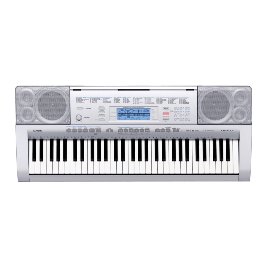
Casio CTK-4000 Service Manual & Parts List
Electronic keyboard
Hide thumbs
Also See for CTK-4000:
- User manual (80 pages) ,
- Appendix (2 pages) ,
- Product catalog (2 pages)

Related Manuals for Casio CTK-4000


Summary of Contents for Casio CTK-4000
- Page 1 (without price) CTK-4000 JUL. 2008 CTK-4000 ELECTRONIC KEYBOARD Ver.2 : Dec. 2008 INDEX...
-
Page 2: Table Of Contents
CONTENTS SPECIFICATIONS ------------------------------------------------------------------------------------------ 1 BLOCK AND WIRING DIAGRAM --------------------------------------------------------------------- 3 PCB LAYOUT ----------------------------------------------------------------------------------------------- 4 CIRCUIT DESCRIPTION --------------------------------------------------------------------------------- 5 PRINTED CIRCUIT BOARDS -------------------------------------------------------------------------- 7 DIAGNOSTIC PROGRAM ------------------------------------------------------------------------------10 EXPLODED VIEW ----------------------------------------------------------------------------------------13 PARTS LIST ------------------------------------------------------------------------------------------------14 SCHEMATIC DIAGRAMS -------------------------------------------------------------------------------17... -
Page 3: Specifications
SPECIFICATIONS Keyboard 61 standard-size keys Touch Response 2 types, Off Maximum Polyphony 48 notes (24 for certain tones) Tones Built-in Tones Sampling Tones Up to 8 (Melody Sampling: 5, Drum Sampling: 3)* Up to 10 seconds Functions Layer, Split Reverb 1 to 10, Off Chorus 1 to 5, Off... - Page 4 Inputs/Outputs USB port TYPE B Sustain/Assignable jack Standard jack (sustain, sostenuto, soft, rhythm start/stop) Phones/Output jack Stereo standard jack Output Impedance: 200Ω, Output Voltage: 4.5V (RMS) MAX Audio In jack Stereo mini jack Input Impedance: 9kΩ, Input Sensitivity: 200mV Power Jack 9V DC Power Supply 2-way...
-
Page 5: Block And Wiring Diagram
BLOCK AND WIRING DIAGRAM KEYBOARD PCB KEYBOARD PCB Keyboard Keyboard (M802-KYA1) (M802-KYA2) CN801 (13pin) CN802 (10pin) CN803 (10pin) CN804 (11pin) MAIN PCB (M804-MDA1) CN2 (13pin) CN3 (15pin) *Not used: 12pin-15pin MA1~ MA18 SRAM(4Mbit) KC5~KC7, FI4~FI7, MD0 ~ MD15 SI4~SI7 KC0~KC4,FI0~FI3,SI0~SI3 MA1~MA23 P2ROM(128Mbit) MD0 ~ MD15... -
Page 6: Pcb Layout
PCB LAYOUT M805-CNB2 PCB M805-CNB1 PCB M804-MDA1 PCB M804-PSA1 PCB M805-CNA1 PCB M802-KYA1 PCB M802-KYA2 PCB Components MAIN PCB M804-MDA1 MPU, Reset IC, SRAM(4Mbit), P2ROM(128Mbit), Key controller, SD card, USB, Power supply circuit SUB PCB M804-PSA1 Power supply circuit, Power amplifer, Phones terminal, Phone terminal, Pedal, DC IN jack Console PCBs M805-CNA1... -
Page 7: Circuit Description
CIRCUIT DESCRIPTION KEY MATRIX ... -
Page 8: Button Matrix
BUTTON MATRIX SW00 SW01 SW02 SW03 SW04 SW05 SW06 SWI0 SAMPLING RECORDER RHYTHM CARD SCALE SONG SWI1 FUNCTION TONE EDITOR BANK RHYTHM SWI2 METRONOME LISTEN WATCH EDITOR TEMPO START/ SWI3 REMEMBER NEXT DOWN STOP CHORDS/ AUTO TEMPO MUSIC SWI4 ACCOMP AUTO SPLIT LAYER... -
Page 9: Printed Circuit Boards
PRINTED CIRCUIT BOARDS Main PCB M804-MDA1 Sub PCB M804-PSA1 Top View Top View Bottom View Bottom View – 7 –... - Page 10 Console PCB M805-CNA1 Console PCB M805-CNA2 Console PCB M805-CNA3 Console PCB M805-CNB1 Top View Console PCB M805-CNB2 Bottom View – 8 –...
- Page 11 Keyboard PCB M802-KYA1 Top View Bottom View Keyboard PCB M802-KYA2 Top View Bottom View – 9 –...
-
Page 12: Diagnostic Program
DIAGNOSTIC PROGRAM Initial Setting 1. Connect the AC adaptor. 2. "Main" volume: MAX 3. Prepare a PC with USB cable connected for USB check. How to start diagnostic program 1. Press and hold the "0", "1" and "2" buttons. 2. - Page 13 2. AC adaptor check Press "3" button. 3:AD1XXX Make sure that a value "XXX" shown in the illustration is in the range of 000 to 3FF. 000 to 3FF Press "3" button. 3:AD3XXX Make sure that a value "XXX" shown in the illustration is in the range of 000 to 1FF.
- Page 14 Windows XP Professional (32- bit) *2: Windows Vista (32- bit) Connect CTK-4000 to the computer with a USB cable. Check that the message "USB AUDIO DEVICE" appears in "Device Manager" → "Sound, Video and Game Controller" on the computer monitor.
-
Page 15: Exploded View
EXPLODED VIEW (-) (+) – 13 –... -
Page 16: Parts List
PARTS LIST CTK-4000 Notes: This parts list does not include the cosmetic parts, which parts are marked with item No. “R-X” in the exploded view. Contact our spare parts department if you need these parts for refurbish. 1. Prices and specifications are subject to change without prior notice. - Page 17 10222381 LSI ST7066U-0A-QG Q2,3 10202670 TRANSISTOR KTA2014-GR-RTK/P 10207675 TRANSISTOR KTC4075-GR-RTK/P 10310579 PCB ASSY/CNB2 TK-RJM508910*001 10273794 VARIABLE RESISTOR F-09KGH1-CASIO-2 Keyboard PCBs 10304697 PCB ASSY/KEY/RUBER TK-RJM508598*001 10304698 PCB ASSY/KYA TK-RJM508618*001 D1-D61 10294400 DIODE LM1MA142WKT1G 61 61 61 61 61 – 15 –...
- Page 18 1 CTK-4000_DI 2 CTK-4000_CHINA 3 CTK-4000_EU 4 CTK-4000_UK 5 CTK-4000_US Q'TY Price Item Parts NO. Parts Name Specification Remarks Code Keyboard Unit 10269451 RUBBER/CONTACT/CB RJM507656-001V01 10270393 RUBBER/CONTACT/CS RJM507657-001V01 10249864 WHITE KEY/CB TK-RJM507243*001 10249865 WHITE KEY/CS TK-RJM507244*001 10274032 BLACK KEY/10P RJM506595-001V02 10247548 BLACK KEY/5P RJM506595-002V01 Case Unit...
-
Page 19: Schematic Diagrams
SCHEMATIC DIAGRAMS Main PCB M804-MDA1 Not used: pin12 to pin15 – 17 –... - Page 20 Sub PCB M804-PSA1 Not used – 18 –...
- Page 21 Console PCB M805-CNA1 – 19 –...
- Page 22 Console PCB M805-CNA2 Console PCB M805-CNA3 – 20 –...
- Page 23 Console PCB M805-CNB1 Console PCB M805-CNB2 – 21 –...
- Page 24 Console PCB M802-KYA1 – 22 –...
- Page 25 Keyboard PCB M802-KYA2 – 23 –...
- Page 26 • Addition of The CIRCUIT DESCRIPTION (P5 to P6) • Correction of The PRINTED CIRCUIT BOARDS (P7 and P8) • Correction of The SCHEMATIC DIAGRAMS (P18 and P20) CASIO COMPUTER CO.,LTD. Overseas Service Division 6-2, Hon-machi 1-Chome Shibuya-ku, Tokyo 151-8543, Japan...