Table of Contents
Advertisement
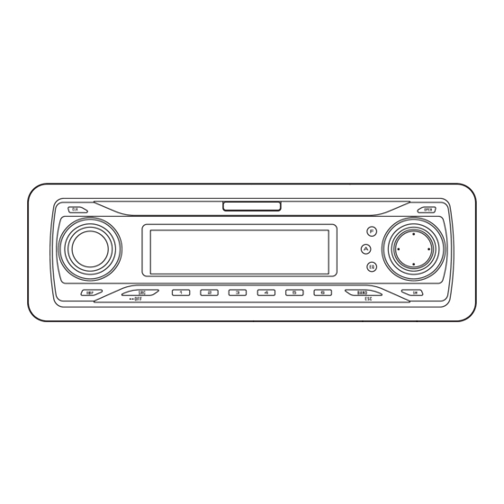
MULTI-CD CONTROL HIGH POWER CD/MP3/WMA/WAV PLAYER WITH FM/AM TUNER
DEH-P5750MP
This service manual should be used together with the following manual(s):
Model No.
Order No.
CX-3158
CRT3394
For details, refer to "Important Check Points for Good Servicing".
PIONEER CORPORATION
PIONEER ELECTRONICS (USA) INC. P.O. Box 1760, Long Beach, CA 90801-1760, U.S.A.
PIONEER EUROPE NV Haven 1087, Keetberglaan 1, 9120 Melsele, Belgium
PIONEER ELECTRONICS ASIACENTRE PTE. LTD. 253 Alexandra Road, #04-01, Singapore 159936
PIONEER CORPORATION 2004
Mech.Module
S10.1AAC
CD Mech. Module:Circuit Description, Mech. Description, Disassembly
4-1, Meguro 1-chome, Meguro-ku, Tokyo 153-8654, Japan
DEH-P5750MP/XM/ES
Remarks
ORDER NO.
CRT3357
/XM/ES
K-ZZD.NOV. 2004 Printed in Japan
Advertisement
Table of Contents

Related Manuals for Pioneer DEH-P5750MP


Summary of Contents for Pioneer DEH-P5750MP
- Page 1 PIONEER CORPORATION 4-1, Meguro 1-chome, Meguro-ku, Tokyo 153-8654, Japan PIONEER ELECTRONICS (USA) INC. P.O. Box 1760, Long Beach, CA 90801-1760, U.S.A. PIONEER EUROPE NV Haven 1087, Keetberglaan 1, 9120 Melsele, Belgium PIONEER ELECTRONICS ASIACENTRE PTE. LTD. 253 Alexandra Road, #04-01, Singapore 159936 PIONEER CORPORATION 2004 K-ZZD.NOV.
-
Page 2: Safety Information
4. After replacing the pickup unit, be sure to check the 2. Before disassembling the unit, be sure to turn off grating. the power. Unplugging and plugging the connectors during power-on mode may damage the ICs inside the unit. DEH-P5750MP/XM/ES... - Page 3 To protect products from damages or failures during transit, the shipping mode should be set or the shipping screws should be installed before shipment. Please be sure to follow this method especially if it is specified in this manual. DEH-P5750MP/XM/ES...
-
Page 4: Table Of Contents
7. GENERAL INFORMATION ..........................53 7.1 DIAGNOSIS ............................. 53 7.1.1 DISASSEMBLY ............................. 53 7.1.2 CONNECTOR FUNCTION DESCRIPTION ..................56 7.2 PARTS..............................57 7.2.1 IC ................................57 7.2.2 DISPLAY ............................... 65 7.3 OPERATIONAL FLOW CHART ....................... 66 7.4 CLEANING............................... 67 8. OPERATIONS ..............................68 DEH-P5750MP/XM/ES... -
Page 5: Specifications
1. SPECIFICATIONS DEH-P5750MP/XM/ES... -
Page 6: Exploded Views And Parts List
22-3 Installation Manual XRD7064 22-4 Caution Card CRP1310 Polyethylene Bag CEG-158 Handle CNC5395 Case Assy CXB3520 ••••• ••••• Owner's Manual,Installation Manual Part No. Language XRD7062 English, Spanish, Portuguese(B) XRD7063 Traditional Chinese, Arabic XRD7064 English, Spanish, Portuguese(B), Traditional Chinese, Arabic DEH-P5750MP/XM/ES... - Page 7 DEH-P5750MP/XM/ES...
-
Page 8: Exterior
2.2 EXTERIOR DEH-P5750MP/XM/ES... - Page 9 XXA7361 FM/AM Tuner Unit CWE1802 Cover CNM6854 Holder CND2144 Insulator XNM7031 Lighting Conductor CNV6487 Spring CBL1512 Detachable Assy XXA7281 CNV6486 Screw BPZ20P100FZK IC(IC901) NJM2388F84 Spring CBL1470 Transistor(Q650,911) 2SD2396 Knob XAA7021 Button(CLK) XAC7062 Choke Coil(L901) CTH1280 IC(IC1802) TSOP4840SB1 Button(DISP) XAC7063 DEH-P5750MP/XM/ES...
-
Page 10: Cd Mechanism Module
2.3 CD MECHANISM MODULE 1GEM1024 2GEM1045 3GEM1035 DEH-P5750MP/XM/ES... - Page 11 CND2712 Bracket CND1895 Screw JFZ20P020FTC CNC9968 Screw JGZ17P022FTC CND1909 ••••• Lever CND2032 Washer YE20FTC Pickup Unit(P10)(Service) CXX1641 Lever CNC9984 Sheet CNM8134 Screw IMS26P030FTC Collar CNV7798 Spring CBL1635 Guide CNV7799 Clamper CNV8372 CNV8403 Rack CNV8374 Holder CNV8376 Holder CNV8377 CNV8378 DEH-P5750MP/XM/ES...
-
Page 12: Block Diagram And Schematic Diagram
VDCONT CD3VON 46 HOME VDCONT VDCONT CLAMP 12EJ DISC SENSE SENSE SENSE SENSE +3.3V REGULATOR Q832 IC 203 IC 703 3VDD S802 V3R3D NJM2391DL1-33 S-812C33AUA-C2N Q641 +3.3V REGULATOR DETACH SENSE SW Q840 CD3VCONT CD3VON Q642 LCDPW Q841 LCD POWER DEH-P5750MP/XM/ES... -
Page 13: Panel Unit
OPT IN TSOP4840SB1 Q832 KDT0-3,KST1-6 DPDT DPDT KEY MATRIX KEY DATA S802 DETACH SENSE SW LCD DRIVER/ X1800 ILLUMINATION KEY CONTROLLER KYDT KYDT IC 1800 COM0-7,SEG0-55 CSENS CSENS PD2072A Q840 BL+B BL+B CN1951 CN1950 Q1861 Q841 ADJ SW LCD POWER DEH-P5750MP/XM/ES... -
Page 14: Overall Connection Diagram(Guide Page)
Code Practical value 0.01uF 12k ohms 101/10 100uF/10V 10k ohms The > mark found on some component parts indicates the importance of the safety factor of the part. Therefore, when replacing, be sure to use parts of identical designation. DEH-P5750MP/XM/ES... - Page 15 L ch > FRONT R ch FRONT L ch FM:+5.6dBs AM: -4.9dBs FM:4.8dBs IP-BUS:+10.3dBs AM:-5.7dBs CD:+10.49dBs IP-BUS:+8.5dBs CD: +9.2dBs SUB WOOFER R ch SUB WOOFER L ch SYSTEM CONTROLLER > FUSE CEK1208 BACK UP DETACH SENSE FM:+31.6dBs AM:+21.1dBs IP-BUS:+36.3dBs CD:+36.49dBs DEH-P5750MP/XM/ES...
- Page 16 FM(100%):-19.5dBs FM/AM TUNER UNIT AM(30%):-30.0dBs DEH-P5750MP/XM/ES...
- Page 17 CD:+0.39dBs DEH-P5750MP/XM/ES...
- Page 18 DEH-P5750MP/XM/ES...
- Page 19 DEH-P5750MP/XM/ES...
-
Page 20: Keyboard Unit
3.3 KEYBOARD UNIT REMOTE CONTROL SENSOR ↑ → FUNC LCD DRIVER, KEY CONTROLLER DISP DEH-P5750MP/XM/ES... - Page 21 KEYBOARD UNIT → ↓ ← VOLUME AUDIO BAND DEH-P5750MP/XM/ES...
-
Page 22: Cd Mechanism Module(Guide Page)
Symbol indicates a capacitor. No differentiation is made between chip capacitors and discrete capacitors. Decimal points for resistor and capacitor fixed values are expressed as : ← ← 0.022 R022 M1 CXC4440 SPINDLE MOTOR M2 CXB8933 LOADING /CARRIAGE CD DRIVER MOTOR DEH-P5750MP/XM/ES... - Page 23 S904:12EJ SWITCH.....ON-OFF S905:8EJ SWITCH....ON-OFF The underlined indicates the switch position. SIGNAL LINE FOCUS SERVO LINE TRACKING SERVO LINE CARRIAGE SERVO LINE SPINDLE SERVO LINE CD CORE UNIT(S10.1) 3.3V REGULATOR SRAMLEVEL2 MICRO COMPUTER 3V REGULATOR CN651 SRAMLEVEL1 SRAMLEVEL0 TYPE_A/D & DEH-P5750MP/XM/ES...
- Page 24 DEH-P5750MP/XM/ES...
- Page 25 DEH-P5750MP/XM/ES...
- Page 26 DEH-P5750MP/XM/ES...
- Page 27 DEH-P5750MP/XM/ES...
- Page 28 7 SIN 500mV/div 200mV/div 1V/div @ TE 500mV/div 9 TIN 500mV/div CD-ROM play operation(Regular track Jump) Spindle waveform during play operation Spindle waveform during play operation (Wider) Ref.: Ref.: Ref.: REFO REFO REFO Mode: Mode: Mode: Normal Normal Normal DEH-P5750MP/XM/ES...
- Page 29 500mV/div 4 LOEJ 3 12SNS 9 TIN 5V/div 5V/div 500mV/div 4 LOEJ 5V/div 12 cm CD Eject operation 8 cm CD Eject operation CD-DA >> CD-ROM mode change(Band key) Ref.: Ref.: Ref.: REFO Mode: Mode: Mode: Normal Normal Normal DEH-P5750MP/XM/ES...
- Page 30 % RFAGC 1V/div 500ms/div 1V/div 500µs/div 8 CIN 9 TIN 500mV/div 1V/div 9 TIN @ TE 500mV/div 1V/div 0 FIN 1V/div CD-ROM >> CD-DA mode change(Band key) Black dot(800µm) during play Ref.: Ref.: REFO REFO Mode: Mode: Normal Normal DEH-P5750MP/XM/ES...
- Page 31 DEH-P5750MP/XM/ES...
-
Page 32: Pcb Connection Diagram
For further information for respective destinations, be sure to check with the schematic dia- gram. 2.Viewpoint of PCB diagrams IP-BUS Capacitor Connector SIDE A SIDE B P.C.Board Chip Part CN901 DETACH SENSE DEH-P5750MP/XM/ES... - Page 33 CORD ASSY SIDE A CORD ASSY ANTENNA CN1950 FRONT DEH-P5750MP/XM/ES...
- Page 34 TUNER AMP ASSY TESTIN DEH-P5750MP/XM/ES...
- Page 35 SIDE B DEH-P5750MP/XM/ES...
-
Page 36: Keyboard Unit
4.2 KEYBOARD UNIT KEYBOARD UNIT SIDE A DEH-P5750MP/XM/ES... - Page 37 KEYBOARD UNIT SIDE B CN1951 DEH-P5750MP/XM/ES...
-
Page 38: Cd Mechamodule Unit
4.3 CD MECHAMODULE UNIT CD CORE UNIT(S10.1) SIDE A LOADING /CARRIAGE MOTOR SPINDLE MOTOR CN651 HOME REFO1 DEH-P5750MP/XM/ES... - Page 39 CD CORE UNIT(S10.1) SIDE B 12EJ DSCSNS DEH-P5750MP/XM/ES...
-
Page 40: Panel Unit
4.4 PANEL UNIT SIDE A PANEL UNIT CN1800 EJECT SIDE B PANEL UNIT CN801 DEH-P5750MP/XM/ES... -
Page 41: Electrical Parts List
RS1/16S102J Q 982 (A,130,100) Transistor UMD2N R 105 (A,46,83) RS1/16S472J D 131 (A,63,66) Diode Network DA204U R 106 (A,47,86) RS1/16S472J D 132 (A,46,70) Diode Network DA204U R 107 (B,25,129) RS1/16S821J D 133 (A,56,61) Diode DAN202U R 108 (B,23,129) RS1/16S223J DEH-P5750MP/XM/ES... - Page 42 R 606 (A,91,65) RS1/16S104J R 932 (B,46,105) RS1/16S472J R 607 (B,64,58) RS1/16S822J R 933 (B,52,102) RS1/16S473J R 608 (A,74,66) RS1/16S102J R 934 (B,54,102) RS1/16S103J R 609 (A,95,45) RS1/16S102J R 935 (B,48,105) RS1/16S473J R 610 (A,80,51) RS1/16S104J R 936 (B,44,99) RS1/16S104J DEH-P5750MP/XM/ES...
- Page 43 Unit Name:Keyboard Assy C 303 (A,105,110) CFTNA224J50 C 304 (A,124,104) CFTNA224J50 MISCELLANEOUS C 309 (A,117,108) CEJQ330M10 IC 1800 (B,28,88) IC PD2072A C 310 (A,126,135) CKSQYB225K10 IC 1802 (A,12,29) IC TSOP4840SB1 C 311 (A,127,131) CKSQYB225K10 IC 1803 (B,20,62) IC BD4834G DEH-P5750MP/XM/ES...
- Page 44 R 1813 (B,34,69) RS1/16S473J R 1814 (B,37,64) RS1/16S473J Unit Number:CWX3096 R 1824 (B,36,42) RS1/16S560J Unit Name:CD Core Unit(S10.1) R 1825 (B,44,124) RS1/16S560J MISCELLANEOUS R 1826 (B,42,119) RS1/16S560J R 1827 (B,39,42) RS1/16S560J R 1828 (B,35,157) RS1/16S560J IC 201 (A,39,24) IC UPD63763GJ DEH-P5750MP/XM/ES...
- Page 45 R 716 (A,63,56) RS1/16SS472J C 243 (B,39,76) CKSSYB104K10 R 719 (B,49,45) RS1/16SS221J R 720 (B,46,52) RS1/16SS471J C 244 (B,49,70) CKSSYB104K10 R 724 (A,62,42) RS1/16S473J C 246 (A,23,19) CKSSYB104K10 C 251 (B,28,31) CKSRYB102K50 R 725 (B,57,43) RS1/16SS222J C 260 (A,54,25) CKSSYB104K10 DEH-P5750MP/XM/ES...
- Page 46 C 716 (A,61,40) CKSSYB103K16 C 722 (B,52,48) CKSQYB475K6R3 C 723 (A,26,41) CKSRYB105K10 C 903 (B,56,70) CKSSYB471K50 C 906 (A,40,77) CKSRYB224K16 C 907 (A,47,76) CKSSYB103K16 C 910 (B,60,71) CKSQYB225K10 Miscellaneous Parts List Pickup Unit(P10)(Service) CXX1641 Motor Unit(SPINDLE) CXC4440 CXB8933 Motor Unit(LOADING/CARRIAGE) DEH-P5750MP/XM/ES...
-
Page 47: Adjustment
1k ohms in series. • The load and eject operation is not guarantied with the mechanism upside down. If the mechanism is blocked due to mistaken eject operation, reset the product or turn off and on the ACC to restore it. DEH-P5750MP/XM/ES... - Page 48 → → TYP(1X) TYP(2X) TRK 22 MIN 22 SEC 22 TRK 11 MIN 11 SEC 11 TRK 11 MIN 11 SEC 11 TRK 22 MIN 22 SEC 22 As for the double speed (2x), audio output cannot be supported DEH-P5750MP/XM/ES...
-
Page 49: Checking The Grating After Changing The Pickup Unit
Because of eccentricity in the disc and a slight misalignment of the clamping center the grating waveform may be seen to "wobble" ( the phase difference changes as the disc rotates). The angle specified above indicates the average angle. • Hint Reloading the disc changes the clamp position and may decrease the "wobble". DEH-P5750MP/XM/ES... - Page 50 Ech → Xch 20mV/div, AC Grating waveform Fch → Ych 20mV/div, AC 0° 30° 45° 60° 75° 90° DEH-P5750MP/XM/ES...
-
Page 51: Error Mode
If TOC can’t be read, error wouldn’t occur, but mechanism still continues its operation. The upper digits of error code is mainly classified by 3 kinds as follows: 1x: Setup related error, 3x: Search related error, Ax: Other errors. DEH-P5750MP/XM/ES... -
Page 52: System Microcomputer Test Program
The frequency of the clock signal is 312.500kHz that is one 32nd of the fundamental frequency. The clock signal should be 312.500kHz ± 13Hz. If the clock signal is out of the range, the X'tal (X601) should be replaced with new one. DEH-P5750MP/XM/ES... -
Page 53: General Information
Grille Assy. Fig.1 Grille Assy Removing the Tuner Amp Assy (Fig.2) Remove the screw. Remove the three screws. Straighten the tabs at three locations indicated. Remove the screw and then remove the Tuner Amp Assy. Tuner Amp Assy Fig.2 DEH-P5750MP/XM/ES... - Page 54 Caution: Before installing the carriage mechanism in the frames, be sure to apply some alcohol to the dampers and set the mechanism to the clamp mode. Carriage Mechanism Damper Lower Frame Damper Damper DEH-P5750MP/XM/ES...
- Page 55 Caution: In assembling, move the planet gear to the load/eject position before setting the feed screw in the inner holder. Washer Pickup Lock Arm Change Arm Styling Holder Feed Screw Inner Holder Planet Gear DEH-P5750MP/XM/ES...
-
Page 56: Connector Function Description
7.1.2 CONNECTOR FUNCTION DESCRIPTION 1 0 A DEH-P5750MP/XM/ES... -
Page 57: Parts
ROM correction : Data input/output EVOL : Strobe output EVOL : Data output EVOL : Clock output IPPW IPBUS : Driver power supply control output ASENBO IPBUS : Slave ACC sense output isens Illumination sense input 82,83 MODEL1,0 Model select input DEH-P5750MP/XM/ES... - Page 58 IC's marked by * are MOS type. Be careful in handling them because they are very liable to be damaged by electrostatic induction. NJM2391DL1-05 NJM2388F84 Bandgap VOUT Reference ON/OFF control VREF Over Voltage Thermal Over Current Protection Protection Protection Thermal Over current CONT Shutdown protector DEH-P5750MP/XM/ES...
- Page 59 76–84 COM0-7 LCD common output 85–90 KST1-6 Key strobe output 91,92 Not used 93-96 V4-1 LCD drive power supply 97,98 C1,C0 Not used Crystal oscillator connection pin * PD2072A HA12240FP BUS+ BUS- BIAS DRIVER OUTPUT RECEIVER OUTPUT BD4834G Vref DEH-P5750MP/XM/ES...
- Page 60 CD mute control output 56-58 Not used CD LSI chip selection output Not used xwait CD LSI write control signal output CLKOUT Internal system clock output(Open) LOCK Spindle lock input Not used xwrite CD LSI write control signal output Not used DEH-P5750MP/XM/ES...
- Page 61 CD-DA analog/digital output change setup input testin Chip check test program starting input HOME Home SW sense input TEMP Temperature information sense input VDSENS VD power supply short sense input Not used * PE5454A Format Meaning CMOS NJM2885DL1-33 Thermal Protection Bandgap Reference DEH-P5750MP/XM/ES...
- Page 62 Output of DRAM ras cas)(LDQM) Output of DRAM lower cas(LDQM) cas!(UDQM) Output of DRAM upper cas(UDQM) Output of DRAM we oe(cas) Output of DRAM oe(cas) D.GND Ground for digital circuits 73-88 RDB0-15 Input/output of DRAM data0-15 89-99 RA0-10 Output of DRAM address0-10 DEH-P5750MP/XM/ES...
- Page 63 Connected to the capacitor for output of REFOUT Reversal input of FE Output of FE ADIN Input of FE, TE A/D converter Reversal input of TE Output of TE Output of LD Input of PD D.GND Ground for digital circuits * UPD63763GJ DEH-P5750MP/XM/ES...
- Page 64 Antenna switch control signal output. “High” : MAIN, ”Low”=SUB control 23 L ch O L channel output FM stereo “L-ch” signal output or AM audio output 24 R ch O R channel output FM stereo “R-ch” signal output or AM audio output DEH-P5750MP/XM/ES...
-
Page 65: Display
COM 0 COM 0 COM 1 COM 1 COM 2 COM 2 COM 3 COM 3 COM 4 COM 4 COM 5 COM 5 COM 6 COM 6 COM 7 COM 7 SEG 52 SEG 53 SEG 54 SEG 55 DEH-P5750MP/XM/ES... -
Page 66: Operational Flow Chart
In case of the above signal, the communication with Grille microcomputer may fail. Source keys If the time interval is not 300msec, the oscillator operative may be defective. Source ON SYSPW←H Pin 1 Completes power-on operation. (After that, proceed to each source operation) DEH-P5750MP/XM/ES... -
Page 67: Cleaning
7.4 CLEANING Before shipping out the product, be sure to clean the following portions by using the prescribed cleaning tools: Portions to be cleaned Cleaning tools CD pickup lenses Cleaning liquid : GEM1004 Cleaning paper : GED-008 DEH-P5750MP/XM/ES... -
Page 68: Operations
8. OPERATIONS DEH-P5750MP/XM/ES... - Page 69 DEH-P5750MP/XM/ES...
- Page 70 DEH-P5750MP/XM/ES...
- Page 71 DEH-P5750MP/XM/ES...
- Page 72 DEH-P5750MP/XM/ES...
- Page 73 DEH-P5750MP/XM/ES...
- Page 74 DEH-P5750MP/XM/ES...
- Page 75 1. Attach the holders to both sides of the front panel. Holder CXX1645 Holder CXX1644 2. Replace the front panel to the unit. 3. Flip the holders into upright positions. 4. Fix the front panel to the unit using fixing screws. Fixing screw CXX1646 DEH-P5750MP/XM/ES...
- Page 76 DEH-P5750MP/XM/ES...
- Page 77 DEH-P5750MP/XM/ES...
- Page 78 - Jigs List Name Jig No. Remarks Test Disc TCD-784 Checking the grating L.P.F. Checking the grating g (Two pieces) DEH-P5750MP/XM/ES...