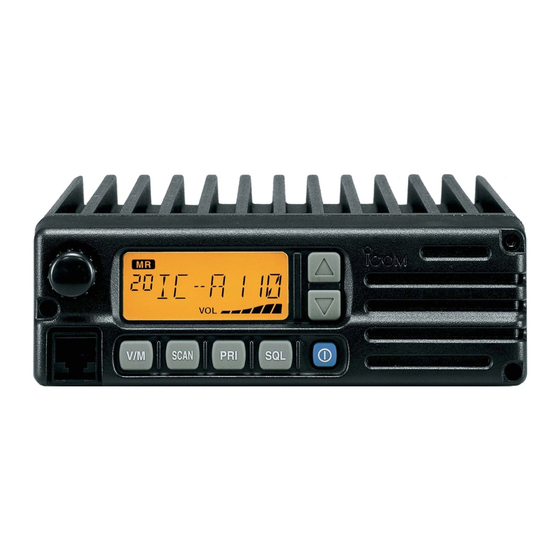
Icom IC-A110 Service Manual
Vhf air band transceiver
Hide thumbs
Also See for IC-A110:
- Instruction manual (24 pages) ,
- Service manual (4 pages) ,
- Price list (158 pages)
Table of Contents
Advertisement
Advertisement
Table of Contents

Related Manuals for Icom IC-A110


Summary of Contents for Icom IC-A110
- Page 1 SERVICE MANUAL VHF AIR BAND TRANSCEIVER iA110...
- Page 2 This service manual describes the latest service informa- NEVER connect the transceiver to an AC outlet or to a DC tion for the IC-A110 VHF AIR BAND TRANSCEIVER at the power supply that uses more than 16 V. This will ruin the time of publication.
-
Page 3: Table Of Contents
TABLE OF CONTENTS SECTION 1 SPECIFICATIONS SECTION 2 INSIDE VIEWS SECTION 3 CIRCUIT DESCRIPTION 3 - 1 RECEIVER CIRCUITS..........................3 - 1 3 - 2 TRANSMITTER CIRCUITS ........................3 - 3 3 - 3 PLL CIRCUITS............................3 - 4 3 - 4 POWER SUPPLY CIRCUITS ........................ - Page 4 SECTION 1 SPECIFICATIONS ‘ ‘ GENERAL • Frequency coverage : 118.000–136.975 MHz • Channel spacing : 25 kHz [GEN], [GEN-1] 25 kHz/8.33 kHz [USA], [USA-1] • Type of emission : AM (6K00A3E) • Number of memory channels : 20 channels : SO-239 (50 Ω) •...
- Page 5 SECTION 2 INSIDE VIEWS ¡MAIN UNIT <TOP VIEW> Power complifier (Q51: MRF137) Low-pass filter Antenna switching circuit APC amplifier (Q11: 2SC4081) Crystal band pass filter (FI2: FL-307 [USA/-1] only) Crystal band pass filter VCO circuit (FI1: FL-306) Ceramic band pass filter TCXO (FI3: CFWM450D) (X1: CR-653)
-
Page 6: Circuit Description
SECTION 3 CIRCUIT DESCRIPTION 3-1 RECEIVER CIRCUITS 3-1-3 1ST MIXER AND 1ST IF CIRCUITS The 1st mixer circuit converts the received signal into a fixed 3-1-1 ANTENNA SWITCHING CIRCUIT frequency of the 1st IF signal with a PLL output frequency. The antenna switching circuit functions as a low-pass filter By changing the PLL frequency, only the desired frequency while receiving. - Page 7 3-1-5 AM DETECTOR CIRCUIT (MAIN UNIT) 3-1-7 SQUELCH CIRCUIT The AM detector circuit converts the 2nd IF signal into AF (MAIN AND FRONT UNITS) signals. The squelch circuit cuts out AF signals when receiving no modulated signal. When no voice modulation is included in The amplified 2nd IF signal from the 2nd IF amplifier (Q6) is the signal, the squelch circuit cuts out the AF signal by com- applied to the AM detector circuit (Q7).
-
Page 8: Transmitter Circuits
3-2 TRANSMITTER CIRCUITS 3-2-3 DRIVE/POWER AMPLIFIER CIRCUITS (MAIN UNIT) 3-2-1 MICROPHONE AMPLIFIER CIRCUIT The amplifier circuit amplifies the VCO oscillating signal to (MAIN UNIT) the output power level. The microphone amplifier circuit amplifies audio signals from the microphone, within +6 dB/octave pre-emphasis The signal from the buffer amplifiers (Q14, Q15) is passed characteristics (300 Hz–3 kHz), to a level needed for the through the TX/RX switch (D11), and is amplified at the pre-... -
Page 9: Pll Circuits
3-3 PLL CIRCUIT 3-3-3 RX LOOP The generated signal at the RX-VCO (Q59, D65) enters the 3-3-1 GENERAL (MAIN UNIT) PLL IC (IC2, pin 8), and is divided at the programmable A PLL circuit provides stable oscillation of the transmit fre- divider section. -
Page 10: Power Supply Circuits
3-5 PORT ALLOCATIONS 3-4 POWER SUPPLY CIRCUITS VOLTAGE LINES (MAIN UNIT) 3-5-1 OUTPUT EXPANDER IC (FRONT unit: IC5) Port LINE DESCRIPTION Description number name The voltage from the external DC power con- nector which is controlled by the power switch Outputs backlight control signals. - Page 11 3-5-2 CPU (FRONT unit; IC1) Port Port Description Description number name number name 1, 2, 3, Input port for the microphone hanger Input ports for the key matrix. 5, 8, 12 HANG detection signal. Low: Microphone on hook. RESET Input port for the CPU reset signal. Input port for the PTT switch.
-
Page 12: Adjustment Procedures
SECTION 4 ADJUSTMENT PROCEDURES 4-1 PREPARATION • Some versions may need the optional CS-A110 and OPC-478, OPC-592 for setting the CLONING SOFTWARE CLONING CABLE adjustment frequency. • All adjustments must be performed on the [Wide] mode. REQUIRED TEST EQUIPMENT EQUIPMENT GRADE AND RANGE EQUIPMENT GRADE AND RANGE... - Page 13 CONNECTION Modulation Attenuator Power supply analyzer 40 dB or 50 dB DC 13.75 V, 10 A RF power meter 50 Ω, 1–50 W Standard signal generator (SSG) 0.1–300 MHz Distortion –127 to –17 dBm (0.1 µV to 32 mV) meter CAUTION! AC millivoltmeter DO NOT transmit...
-
Page 14: Pll Adjustment
4-2 PLL ADJUSTMENT ADJUSTMENT MEASUREMENT POINT ADJUSTMENT ADJUSTMENT CONDITION VALUE UNIT LOCATION UNIT ADJUST • Operating frequency : MAIN Connect a digital 13.5 V MAIN R392 VOLTAGE 118.000 MHz multi-meter to drain • Receiving terminal of Q51. PLL LOCK • Operating frequency : MAIN Connect a digital 0.5 V... - Page 15 pin 2 ( MICE) Audio generator pin 4 ( GND) pin 3 ( MIC) pin 5 ( PTT) J6, pin 3 DC power supply Audio input point 13.75 V/10 A R336 Head set modulation adjustment Vdd voltage check point TUNE voltage adjustment TUNE voltage check point R150 Output power adjustment...
-
Page 16: Receiver Adjustment
4-4 RECEIVER ADJUSTMENT “SQUELCH ADJUSTMENT” must be performed at “SQUELCH ADJUSTMENT MODE”. ADJUSTMENT MEASUREMENT POINT ADJUSTMENT ADJUSTMENT CONDITION VALUE UNIT LOCATION UNIT ADJUST • Operating frequency : Rear Connect an AC milli- Maximum AF output MAIN L9, L10, SENSITIVITY 118.000 MHz panel voltmeter and dis- level... - Page 17 DC power supply 13.75 V/10 A RX sensitivity adjustment 4 - 6...
-
Page 18: Parts List
SECTION 5 PARTS LIST [FRONT UNIT] [FRONT UNIT] ORDER ORDER DESCRIPTION DESCRIPTION 1140008780 S.IC HD6433823A19D 4030006860 S.CERAMIC C1608 JB 1H 102K-T-A 1130009110 S.IC S-80942ANMP-DD6-T2 4030007090 S.CERAMIC C1608 CH 1H 470J-T-A 1130007110 S.IC TC7W04FU (TE12L) 4030006850 S.CERAMIC C1608 JB 1H 471K-T-A 1130008670 S.IC 25LC160T-I/SN 4030006850 S.CERAMIC... - Page 19 [MAIN UNIT] [MAIN UNIT] ORDER ORDER DESCRIPTION DESCRIPTION 1130008830 S.IC TB31207AFN (EL) 1590000430 S.TRANSISTOR DTC144EUA T106 1110003670 S.IC BA3308F-T1 1590000430 S.TRANSISTOR DTC144EUA T106 1110002750 S.IC TA75S01F (TE85R) 1510000770 S.TRANSISTOR 2SA1586-GR (TE85R) 1130004200 S.IC TC4S66F (TE85R) 1530002850 S.TRANSISTOR 2SC4116-BL (TE85R) 1180000800 S.IC S-81350HG-KD-T1 Q100 1590002870 S.FET...
- Page 20 [MAIN UNIT] [MAIN UNIT] ORDER ORDER DESCRIPTION DESCRIPTION ERJ3GEYJ 150 V (15 Ω) 6140000670 COIL LR-89 7030003220 S.RESISTOR ERJ3GEYJ 150 V (15 Ω) 6200004480 S.COIL MLF1608D R82K-T 7030003220 S.RESISTOR ERJ3GEYJ 150 V (15 Ω) 6200009080 S.COIL MC152-E558CN-100025=P3 7030003220 S.RESISTOR 6200004850 S.COIL MC152-E558CN-100024 7030003480 S.RESISTOR ERJ3GEYJ 222 V (2.2 kΩ)
- Page 21 [MAIN UNIT] [MAIN UNIT] ORDER ORDER DESCRIPTION DESCRIPTION R236 7030003600 S.RESISTOR ERJ3GEYJ 223 V (22 kΩ) R406 7030003470 S.RESISTOR ERJ3GEYJ 182 V (1.8 kΩ) R237 7030003600 S.RESISTOR ERJ3GEYJ 223 V (22 kΩ) R407 7030003700 S.RESISTOR ERJ3GEYJ 154 V (150 kΩ) R238 7030003600 S.RESISTOR ERJ3GEYJ 223 V (22 kΩ)
- Page 22 [MAIN UNIT] [MAIN UNIT] ORDER ORDER DESCRIPTION DESCRIPTION 4030007080 S.CERAMIC C1608 CH 1H 390J-T-A C118 4030009630 S.CERAMIC C1608 JB 1H 822K-T-A 4030007040 S.CERAMIC C1608 CH 1H 180J-T-A C119 4030007130 S.CERAMIC C1608 CH 1H 101J-T-A 4030007100 S.CERAMIC C1608 CH 1H 560J-T-A C120 4030012610 S.CERAMIC C2012 JB 1C 474K-T-A...
- Page 23 [MAIN UNIT] [MAIN UNIT] ORDER ORDER DESCRIPTION DESCRIPTION C288 4030006860 S.CERAMIC C1608 JB 1H 102K-T-A C403 4030012600 S.CERAMIC C2012 JB 1A 105M-T-A C289 4030011600 S.CERAMIC C1608 JB 1C 104KT-N C404 4030012610 S.CERAMIC C2012 JB 1C 474K-T-A C290 4030011600 S.CERAMIC C1608 JB 1C 104KT-N C405 4030009350 S.CERAMIC C1608 CH 1H 3R5B-T-A...
- Page 24 [MAIN UNIT] ORDER DESCRIPTION C538 4030007140 S.CERAMIC C1608 CH 1H 121J-T-A C539 4030007010 S.CERAMIC C1608 CH 1H 100D-T-A C540 4030006860 S.CERAMIC C1608 JB 1H 102K-T-A C541 4030011600 S.CERAMIC C1608 JB 1C 104KT-N C542 4030011600 S.CERAMIC C1608 JB 1C 104KT-N C543 4030011600 S.CERAMIC C1608 JB 1C 104KT-N C544...
-
Page 25: Mechanical Parts And Dissasembly
SECTION 6 MECHANICAL PARTS AND DISSASEMBLY [CHASSIS PARTS] [ACCESSORIES] REF. NO ORDER NO. DESCRIPTION QTY. REF. NO ORDER NO. DESCRIPTION QTY. 6510004880 Connector MR-DS-E 01 5210000070 Fuse FGB 10A 8010017870 2270 chassis Optional product DC power cable OPC-344 Screw PH BT M3 × 8 NI-ZU 8810008660 8900000730 Microphone (HANG) cable OPC-049... - Page 26 OPPOSITE DIRECTION TO THE MAIN UNIT MP12 (M) MP4 (C) MP4 (M) J1 (C) MP11 (M) MP12 (C) W1 (M) MP5 (M) MP9 (M) MP3 (C) MP17 (C) FRONT UNIT MP6 (M) MP2 (M) MP2 (C) MP10 (F) MP6 (C) MP2 (C) MP8 (M) EP2 (F)
-
Page 27: Semi-Conductor Information
SECTION 7 SEMI-CONDUCTOR INFORMATION • • TRANSISTORS AND FET’S DIODES 1SS352 1SV271 1SV307 DA204 U T107 DE5SC6M-4061 2SA1471R 2SA1586 GR 2SA1622 6 TL 2SB1132 T100 R 2SB798 T2 DK (Symbol: SG) (Symbol: M6) (Symbol: BART) (Symbol: DK) (Symbol: C1) (Symbol: TG) (Symbol: TX) (Symbol: K) (Symbol: 5SC6) -
Page 28: Board Layouts
SECTION 8 BOARD LAYOUTS 8-1 FRONT UNIT The combination of this page and the next page show the unit layout in the same configuration as the actual P.C.Board. ¡TOP VIEW HANG MICE CLON 8 - 1... - Page 29 ¡BOTTOM VIEW RMUT AFMUT SMUT BEEP FROM MAIN FISW UNIT J5 TMUT UNLK PSWC PLSTB CPU5V MICE PDET PTTS SQLI 8 - 2...
- Page 30 8-2 MAIN UNIT EXT SP The combination of this page and the next page show the unit layout in the same configuration as the actual ¡TOP VIEW P.C.Board. TO FRONT UNIT J1 8 - 3...
- Page 31 ¡BOTTOM VIEW 8 - 4...
-
Page 32: Main Unit
SECTION 9 BLOCK DIAGRAM [ ANT ] 1st MIX D51~D52 1st IF=38.85MHz 2nd IF=450KHz 1SV271 X2 D50: 1SV271 Q4~Q5 D44: MA8051 D7,D8 D6,D37 D1~D3 2SC4211 2SC4215 2SC4215 X2 CFWM450D IC40: TA31136FN Q3: 2SC4215 1SV307 FL-306 1SV307 3SK184 HVU350 X2 3SK184 HVU350 X2 1SV271 UM9401F X3... -
Page 33: Voltage Diagram
SECTION 10 VOLTAGE DIAGRAM 10-1 FRONT UNIT Dimmer OFF : 0V Light : 7.8V Dark : 6.1V HLC7453-012400 Dimmer OFF : 0V Light : 7.8V Dark : 6.1V DTA143ZU DTC114EU CL-170Y-CD CL-170Y-CD CL-170Y-CD DTA143ZU DTC114EU CL-170Y-CD CL-170Y-CD CL-170Y-CD Dimmer OFF : 0V 2SA1622 LED2 LED2... -
Page 34: Main Unit
10-2 MAIN UNIT C333 R447 R448 FL-306 Note 1SV307 0.01 1.2k 1SV307 R377 TX: 0 V U : [USA/-1] only 0.5p 0.001 RX: 5.6 V TX: 0.39 V C255 RX: 2.08 V 0.001 RF AGC LS-527 LS-527 TX: 0 V C318 RX: 5.9 V 0.01... - Page 35 CHASSIS MOD V (W36) MOD V (ANT) TX: 0 V HK-08S070- HK-08S070- HK-08S070- RX: 5.6 V TX: 0 V TX: 0.39 V 1310 1310 1310 ZBFS5101-PT RX: 2.08 V RX: 1.7 V C358 C342 C165 C362 RF AGC 0.75p 1SV271 0.001 LA-244 LA-244...
- Page 36 10-2 MAIN UNIT CHASSIS MOD V (W36) MOD V C333 R447 R448 Note FL-306 1SV307 0.01 1.2k 1SV307 R377 (ANT) TX: 0 V U : [USA/-1] only 0.5p 0.001 RX: 5.6 V TX: 0.39 V TX: 0 V HK-08S070- HK-08S070- HK-08S070- 1310 1310...
- Page 37 290-294 Albert Street, Brunswick, Victoria, 3056, Australia : http://www.icomuk.co.uk Phone : 03 9387 0666 Fax : 03 9387 0022 : http://www.icom.net.au Zac de la Plaine, Rue Brindejonc des Moulinais BP 5804, 31505 Toulouse Cedex, France 6F No. 68, Sec. 1 Cheng-Teh Road, Taipei, Taiwan, R.O.C.
- Page 38 S-13608HI-CD 6-9-16, Kamihigashi, Hirano-ku Osaka 547-0002, Japan c 2000 Icom Inc.