Advertisement
Table of Contents
- 1 Table of Contents
- 2 Micro Component System
- 3 Preventing Static Electricity
- 4 Important for Laser Products
- 5 Disassembly Method
- 6 Main Adjustment
- 7 Maintenance of Laser Pickup
- 8 Replacement of Laser Pickup
- 9 Description of Major Ics
- 10 Internal Connection of Display
- Download this manual
See also:
Instruction Manual
SERVICE MANUAL
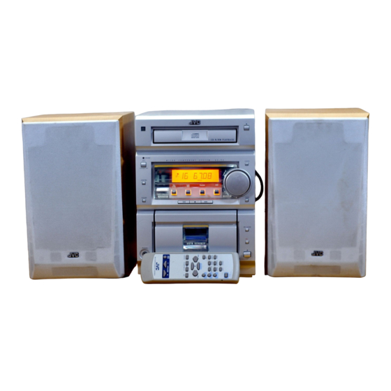
MICRO COMPONENT SYSTEM
STANDBY/ON
DISPLAY
SLEEP
AUX
PROG
RANDOM
REPEAT
SOUND
AUTO
FM/AM
MODE
PRESET
FM MODE
CD
TAPE
CD
CANCEL
MULTI KEY
SET
AHB
PRO
VOLUME
RM-SUXP3U REMOTE CONTROL
Contents
Safety precautions
Flow of functional operation
until TOC read (CD)
COMPACT
DIGITAL AUDIO
STANDBY
M I C R O
C O M P O N E N T
S Y S T E M
STANDBY
/
ON
AHB PRO
CD
TAPE
FM/AM
/
DIRECT OPERATING
FUNCTION
SOUND
A U T O R E V E R S E
AUTO TAPE SELECTOR
PHONES
SP-UXP3
CA-UXP3
1-2
1-4
1-6
1-7
1-14
1-18
COPYRIGHT
2001 VICTOR COMPANY OF JAPAN, LTD.
C D - R / R W P L A Y B A C K
U X · P 3
CLOCK
AUX
VOLUME
TIMER
REV .MODE
REC
SP-UXP3
UB
UP
US
UW
UY
UX-P3
UX-P3
Area Suffix
Hong Kong
Korea
Singapore
South Africa
Argentina
1-19
1-19
1-20
1-39
No.20984
1-1
Jun. 2001
Advertisement
Table of Contents

Related Manuals for JVC UX-P3


Summary of Contents for JVC UX-P3
-
Page 1: Table Of Contents
UX-P3 UX-P3 SERVICE MANUAL MICRO COMPONENT SYSTEM UX-P3 COMPACT DIGITAL AUDIO C D - R / R W P L A Y B A C K STANDBY M I C R O C O M P O N E N T S Y S T E M U X ·... - Page 2 UX-P3 1. This design of this product contains special hardware and many circuits and components specially for safety purposes. For continued protection, no changes should be made to the original design unless authorized in writing by the manufacturer. Replacement parts must be identical to those used in the original circuits. Services should be performed by qualified personnel only.
- Page 3 UX-P3 (U.K only) 1. This design of this product contains special hardware and many circuits and components specially for safety purposes. For continued protection, no changes should be made to the original design unless authorized in writing by the manufacturer.
-
Page 4: Preventing Static Electricity
UX-P3 Preventing static electricity Electrostatic discharge (ESD), which occurs when static electricity stored in the body, fabric, etc. is discharged, can destroy the laser diode in the traverse unit (optical pickup). Take care to prevent this when performing repairs. 1.1. Grounding to prevent damage by static electricity Static electricity in the work area can destroy the optical pickup (laser diode) in devices such as DVD players. - Page 5 UX-P3 1.3. Cautions on removing the CD traverse unit * For removing the CD traverse unit in detail, refer to the "Adjustment Method" section of this manual. 1. Before disconnecting the flexible wire from the connector CN601 on the CD SERVO board, solder the part shown in the figure below.
-
Page 6: Important For Laser Products
UX-P3 Important for laser products 5.CAUTION : If safety switches malfunction, the laser is able 1.CLASS 1 LASER PRODUCT to function. 2.DANGER : Invisible laser radiation when open and inter 6.CAUTION : Use of controls, adjustments or performance of lock failed or defeated. Avoid direct exposure to beam. -
Page 7: Disassembly Method
UX-P3 Disassembly method Metal cover <Main body> Removing the metal cover (See Fig.1 and 2) Remove the six screws A on the back of the body. Remove the two screws B on the side of the body. Pull both sides of the metal cover outward and lift the rear part of the cover. - Page 8 UX-P3 Removing the tuner board (See Fig.4 and 5) Tuner board Prior to performing the following procedure, remove the metal cover. Disconnect the card wire from connector CN1 on the tuner board. Remove the screw D on the right side of the body.
- Page 9 UX-P3 Remove the rear panel (See Fig.8 to 11) Joint a Joint a Prior to performing the following procedure, remove the metal cover, rear cover and the CD mechanism assembly. Remove the five screws G attaching the rear panel. Disconnect the card wire from CN902 on the main board.
- Page 10 UX-P3 CN931 Removing the main board / heat sink CN901 (See Fig.13 to 15) CN900 Prior to performing the following procedure, remove Main board the metal cover, the rear cover, the CD mechanism assembly and the rear panel. Disconnect the card wire from connector CN900, CN901 and CN931 on the main board.
- Page 11 UX-P3 Removing power transformer J1000 assembly (See Fig.16 and 17) Prior to performing the following procedure, remove the metal cover, the rear cover, the CD mechanism assembly and the rear panel. Remove the cord stopper upwards on the back of the body.
- Page 12 UX-P3 Front panel assembly Removing the display board / switch board (See Fig.20 to 22) Prior to performing the following procedure, remove the front panel assembly. VOLUME knob Pull out the VOLUME knob on the front panel. Remove the fifteen screws M attaching the display board and the switch board on the back ofthe front panel.
- Page 13 UX-P3 Removing the headphone board (See Fig.23) Display board Prior to performing the following procedure, remove the front panel assembly. Remove the screw O on the back of the front panel. Band If necessary, remove the band bundling the wire extending from the headphone board and the display board.
-
Page 14: Main Adjustment
UX-P3 Main adjustment Tuner section Measurement Instruments Required for Adjustment B/E/EN version 1. Low frequency oscillator FM Band cover: 87.5 108MHz This oscillator should have a capacity to output MW Band cover: 522 1,629kHz 0dBs to 600 at an oscillation frequency of... - Page 15 UX-P3 << >> Arrangement of Adjusting Position Cassette mechanism section Cassette mechanism section (Back side) Head azimuth Head azimuth adjusting screw adjusting screw (Forward side) (Reverse side) Head azimuth Head azimuth Playback/Recording & adjusting screw adjusting screw eraser head (Forward side)
- Page 16 UX-P3 Tape Recorder Section Measurement Adjusting Standard Items Measurement method conditions positions Values Adjust the head Confirmation Test tape 1 Playback the test tape VTT703L (8kHz) Maximum azimuth screw of head angle : VTT703L (8kHz) 2 With the recording & playback mechanism,...
- Page 17 UX-P3 Electrical Performance Adjusting Measurement Standard Items Measurement method positions conditions Values VR31 AC-225 Adjustment of Mode: Forward or 1 With the recording and playback : 4.20 recording bias reverse mode mechanism, load the test tapes (AC-514 to AC-514 current...
- Page 18 UX-P3 Flow of functional operation until TOC read (CD) Check Point Slider turns REST Power Key Power ON Check that the voltage at the pin4 SW ON. of CN601 is 0V (a moment)? Automatic tuning of TE offset Check that the voltage at the...
-
Page 19: Maintenance Of Laser Pickup
UX-P3 Maintenance of laser pickup Replacement of laser pickup (1) Cleaning the pick up lens Befor you replace the pick up, please try to Turn off the power switch and,disconnect the clean the lens with a alcohol soaked cotton power cord from the ac outlet. -
Page 20: Description Of Major Ics
UX-P3 Description of major ICs UPD780058 (IC931 ) : Main micon 1. Pin layout 80 ~ 25 ~ 2. Pin function Port Name Function Function SAFETY0 Irregular voltage detection 0 P15/AN15 Safety DOOR_RST REST/CLOSE switch detect port P16/AN16 Door P17/AN17... - Page 21 UX-P3 Port Name Function Function LEDRV P64/RD Lite LED indicate Reverse LED_REC Lite LED indicate REC P65/WR LEDFR Lite LED indicate Forward P66/WAIT P67/ASTB STTA Tape IC Strobe Tape LCDAT LCD data P30/TO0 LMODE P31/TO1 LCD date mode control LCDCK...
- Page 22 UX-P3 LA6541 (IC801) : Foucus & Spindle & Feed & Tracking BTL driver 1. Pin Layout & block diagram Vref Vin4 Vin3 Level B T L B T L Level RESET shift driver driver shift Level B T L B T L...
- Page 23 UX-P3 MN662748RPM (IC651) : Digital servo & digital signal processer 1. Pin layout 20 ~ 41 ~ 2.Block diagram AVSS1 LRCKIN(MSEL) 8TIMES AVDD1 BCLK(SSEL) DIGITAL OVER SAMPUNC OUTR SRDATAIN DEEMPHSIS 1BIT DIGITAL FILTER (PSEL) LOGIC IOSEL CLVS BLKCK OUTL CLDCK...
- Page 24 UX-P3 3. Pin function Symbol I/O Function Symbol I/O Function Not used Tracking error shunt signal output (H:shunt) BCLK Not used LRCK PLAY Not used SRDATA WVEL Not used Not used DVDD1 Power supply (Digital) RF signal input DVSS1 Connected to GND...
- Page 25 UX-P3 BA15218F-XE (IC904) : Dual operation amplifier 1. Pin layout OUT1 1 8 Vcc -IN1 2 7 OUT2 +IN1 3 6 -IN2 VEE 4 5 +IN2 2. Block diagram OTHER Q114 OUTPUT 1-25...
- Page 26 UX-P3 KIA78S06P-T (IC933) : Regulator 1. Pin layout 2. Block diagram 3 INPUT 1 2 3 1 OUTPUT 2 COMMON 1-26...
- Page 27 UX-P3 LA4628 (IC905) : Power amp 1. Pin layout 10 11 12 13 14 2.Block diagram -OUT GND1 +OUT -OUT GND2 +OUT 1-27...
- Page 28 UX-P3 AN22000A(IC601):RF & SERVO AMP 1. Pin layout 2. Block RF IN OFTR RF OUT C.AGC CBDO COFTR OFTR RF_EQ 3TENV NRFDET 3TOUT NRFDET SUBT FEOUT SUBT TEOUT TEBPF VDET VDET VREF GCTL TBAL FBAL CDDG VCC 3. Function Symbol...
- Page 29 UX-P3 LA1838 (IC1): FM AM IF AMP&detector, FM MPX decoder 1. Block Diagram DECODER RF.AMP ANIT-BIRDIE MUTE BUFF STEREO P-DET AM IF PILOT 384KHz COMP S-METER AM/FM S-CLRVE S-METER IF-BUFF TUNING STEREO DRIVE DRIVE FM IF 2. Pin Function Symbol...
- Page 30 UX-P3 LC72136N (IC2) : PLL frequency synthesizer 1. Pin layout FM/AM LPFOUT LPFIN CLOCK FM/ST/VCO FMIN AM/FM AMIN IFCONT SDIN IFIN 2. Block diagram Phase Reference Detector Driver Charge Pump Swallow Counter Swallow Counter 1/16,1/17 4bit 1/16,1/17 4bit Unlock Detector...
- Page 31 UX-P3 LC72723(IC3):RDS Pin Assignment Block diagram VREF FLOUT CIN Vdda CLOCK Vddd RECOVERY REFERENCE (57kHz) (1187.5kHz) VOLTAGE Vssa VREF Vssd 57kHz ANTIALIASING DATA SMOOTHING RDDA MPXIN (SCF) FILTER FILTER DECODER RDCL MDDE (128-bits) CLK(4.332MHz) RDS-ID RDS-ID/ TEST TEST DETECT READY XDUT 3.
- Page 32 UX-P3 LB1641 (IC802) : DC Motor driver 1. Pin layout GND OUT1 P1 IN2 VCC1 VCC2 P2 OUT2 2. Pin function Input Output Mode OUT1 OUT2 Brake CLOCKWISE COUNTER-CLOCKWISE Brake BU4094BC(IC33):Serial to parallel port extension 1.Pin layout 2.Block diagram STROBE...
- Page 33 UX-P3 BA3126N(IC31) : R/P Switch GP1U26X (IC933) 1-33...
- Page 34 UX-P3 NJU6433FG1 (IC934) 1. Pin layout 2. Bock diagram Common Latch Circuit/Segment Driver Driver Divider Input Input Input Input Shift Register 4 Shift Register 3 Shift Register 2 Circuit Shift Register 1 Switching Switching Switching Switching Circuit Circuit Circuit Circuit...
- Page 35 UX-P3 LC75345M (IC901) 1. Pin layout 2. Block Diagram 1-35...
- Page 36 UX-P3 3. Descriptions Pin name Pin No. Descriptions Input signal pin LSEL0 Input selector output pin. RSEL0 LBASS1 LBASS2 RBASS1 Capacitor and resistor connection pins comprising filters for RBASS2 bass and super-bass band. ATT + equalizer output pin/capacitor connection pin...
- Page 37 UX-P3 Pin name Pin No. Descriptions VDD voltage generation block for analog ground. Vref Capacitor of several 10 F to be connected between Vref and AWSS (VSS) as a counter-measure against power ripple. Ground pin Supply pin Chip enable pin.
- Page 38 UX-P3 AN7317 (IC32) : PB/REC amp 1-38...
-
Page 39: Internal Connection Of Display
UX-P3 Internal connection of display QLD0160-001 (D1934) 1-39... - Page 40 UX-P3 <<MEMO>> 1-40...
- Page 41 UX-P3 UX-P3 VICTOR COMPANY OF JAPAN, LIMITED AUDIO & COMMUNICATION BUSINESS DIVISION PERSONAL & MOBILE NETWORK BUSINESS UNIT 10-1,1Chome,Ohwatari-machi,Maebashi-city,371-8543,Japan 1-41 No.20984 200106(O)