Table of Contents
Advertisement
SERVICE MANUAL
Ver 1.0 2001.04
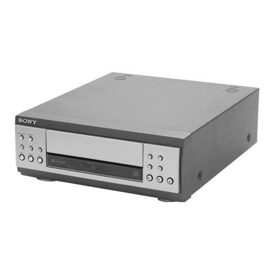
CDP-S3 is the CD player section
in MHC-S7AV or MHC-S3.
Sony Corporation
9-873-831-11
2001D0500-1
Home Audio Company
C 2001.4
Shinagawa Tec Service Manual Production Group
Model Name Using Similar Mechanism
CD Mechanism Type
Base Unit Name
Optical Pick-up Name
SPECIFICATIONS
System
Compact disc and digital
audio system
Laser
Semiconductor laser
(λ=780 nm)
Emission duration:
continuous
Frequency response
2 Hz – 20 kHz (±0.5 dB)
Signal-to-noise ratio
More than 90 dB
Dynamic range
More than 90 dB
OPTICAL OUT
(Square optical connector jack, rear panel)
Dimensions (w/h/d)
Approx. 280 x 108 x 330 mm
Mass
Approx. 2.7 kg
Design and specifications are subject to change
without notice.
CDP-S3
AEP Model
UK Model
Australian Model
NEW
CDM63B-30BD60
BU-30BD60
OP Assy (A-MAX.3)
COMPACT DISC PLAYER
E Model
Advertisement
Table of Contents

Related Manuals for Sony CDP-S3


Summary of Contents for Sony CDP-S3
- Page 1 CDP-S3 SERVICE MANUAL AEP Model UK Model Ver 1.0 2001.04 E Model Australian Model CDP-S3 is the CD player section in MHC-S7AV or MHC-S3. Model Name Using Similar Mechanism CD Mechanism Type CDM63B-30BD60 Base Unit Name BU-30BD60 Optical Pick-up Name OP Assy (A-MAX.3)
- Page 2 LINE WITH MARK 0 ON THE SCHEMATIC DIAGRAMS AND IN THE PARTS LIST ARE CRITICAL TO SAFE OPERATION. REPLACE THESE COMPONENTS WITH SONY PARTS WHOSE PART NUMBERS APPEAR AS SHOWN IN THIS MANUAL OR IN SUPPLEMENTS PUB- LISHED BY SONY.
-
Page 3: Table Of Contents
CDP-S3 TABLE OF CONTENTS SERVICING NOTES ..........4 GENERAL ..............5 DISASSEMBLY 3-1. Disassembly Flow ............6 3-2. Cover ................7 3-3. CD Mechanism Deck (CDM63B-30BD60) ....7 3-4. MAIN Board ..............8 3-5. Front Panel Section ............8 3-6. PANEL (L) Board, PANEL (R) Board ......9 3-7. -
Page 4: Servicing Notes
CDP-S3 SECTION 1 SERVICING NOTES This set is a component of the MHC-S7AV or MHC-S3. CD-TEXT TEST DISC The MHC-S7AV or MHC-S3 system configuration is as shown below, and therefore it does not operate normally unless all four This unit is able to display the test data (character information) components are connected. -
Page 5: General
CDP-S3 SECTION 2 This section is extracted from instruction manual. GENERAL Parts Identification The items are arranged in alphabetical order. Refer to the pages indicated in parentheses ( ) for details. Main unit Remote Control wj wkwl e; ea 1 2 3... -
Page 6: Disassembly
CDP-S3 SECTION 3 DISASSEMBLY • This set can be disassembled in the order shown below. 3-1. DISASSEMBLY FLOW 3-2. COVER (Page 7) 3-3. CD MECHANISM DECK 3-5. FRONT PANEL SECTION 3-4. MAIN BOARD (CDM63B-30BD60) (Page 8) (Page 8) (Page 7) 3-6. -
Page 7: Cover
CDP-S3 Note: Follow the disassembly procedure in the numerical order given. 3-2. COVER 2 screw 3 cover (BVTT3 × 6) 1 two screws (case 3 TP2) 1 two screws (case 3 TP2) 3-3. CD MECHANISM DECK (CDM63B-30BD60) 4 CD mechanism deck... -
Page 8: Main Board
CDP-S3 3-4. MAIN BOARD 2 two connectors (CN101, 102) 1 wire (flat type) (21 core) (CN301) 5 MAIN board 2 connector (CN401) 3 screw (BVTP3 × 8) 3 two screws (BVTP3 × 8) 4 lug 3 screw (BVTP3 × 8) -
Page 9: Panel (L) Board, Panel (R) Board
CDP-S3 3-6. PANEL (L) BOARD, PANEL (R) BOARD 4 four screws (BVTP2.6 × 8) 6 PANEL (R) board 5 two claws 1 five screws (BVTP2.6 × 8) 3 PANEL (L) board 2 two claws 3-7. LID (CD) 2 bracket (LID) assy 1 screw (BVTP2.6 ×... -
Page 10: Test Mode
Note: Use flowing buttons in the test mode. [CD Service Mode] no mark : Button of CD unit (CDP-S3) • This mode can run the CD sled motor optionally. Use this mode, : Button of amplifier unit (TA-S7AV or TA-S3) for instance, when cleaning the optical pick-up. -
Page 11: Electrical Adjustments
CDP-S3 SECTION 5 ELECTRICAL ADJUSTMENTS Note : E-F Balance (1 Track jump) Check 1. CD Block is basically designed to operate without adjustment. Therefore, check each item in order given. oscilloscope BD board 2. Use LUV-P01 (4-999-032-01) unless otherwise indicated. -
Page 12: Diagrams
CDP-S3 SECTION 6 DIAGRAMS 6-1. NOTE FOR PRINTED WIRING BOARDS AND SCHEMATIC DIAGRAMS (In addition to this, the necessary note is printed in each block) Note on Printed Wiring Boards: Note on Schematic Diagram: • All capacitors are in µF unless otherwise noted. pF: µµF •... - Page 13 CDP-S3 • Circuit Boards Location PANEL (R) board MAIN board PANEL (L) board TRAY SENSOR board IN OUT SW board DRIVER board BD board MOTOR board DISC SENSOR board...
-
Page 14: Printed Wiring Board - Bd Section
CDP-S3 6-2. PRINTED WIRING BOARD – BD Section – • See page 13 for Circuit Boards Location. (Page 18) MAIN BOARD CN301 M102 (SLED) M101 (SPINDLE) (RFDC) (FEO) (DVC) (RFAC) (FEI) • Semiconductor Location Ref. No. Location D101 IC101 IC102... -
Page 15: Schematic Diagram -Bd Section
CDP-S3 6-3. SCHEMATIC DIAGRAM – BD Section – • • See page 22 for Waveforms. See page 22 for IC Block Diagrams. (RFAC) TP (DVC) (RFDC) (TEO) IC B/D IC B/D (FEO) IC B/D MAIN BOARD CN301 (Page 19) • Voltages and waveforms are dc with respect to ground Note: The components identified by mark 0 or dotted line under no-signal conditions. -
Page 16: Printed Wiring Boards - Cd Changer Section
CDP-S3 6-4. PRINTED WIRING BOARDS – CD CHANGER Section – • See page 13 for Circuit Boards Location. MAIN BOARD NO202 (Page 18) There are a few cases that the part isn't mounted in model is printed on diagrams. - Page 17 CDP-S3 6-5. SCHEMATIC DIAGRAM – CD CHANGER Section – • See page 22 for IC Block Diagram. IC731 SUB TRAY1 HEIGHT SENSOR IC732 SUB TRAY2 HEIGHT SENSOR IC733 SUB TRAY3 HEIGHT SENSOR MAIN BOARD NO202 (Page 19) IC751 DISC IN DETECT •...
-
Page 18: Printed Wiring Board - Main Section
CDP-S3 6-6. PRINTED WIRING BOARD – MAIN Section – • See page 13 for Circuit Boards Location. (Page 14) (Page 16) SYSTEM CONTROL 3 BD BOARD DRIVER BOARD TO ST-S3/S5 CN101 CN701 MAIN BOARD (CHASSIS) SYSTEM CONTROL 5 TO TC-S3... -
Page 19: Schematic Diagram - Main Section
CDP-S3 6-7. SCHEMATIC DIAGRAM – MAIN Section – • See page 22 for Waveform. OPTICAL OUT TO ST-S3/S5 CLP102 C122 CN301 IC102 0.022 TOTX140 PWM3 CD301 C103 C102 C101 C125 OPTICAL (CHASSIS) PWM2 C301 0.47 CD302 D502 D501 TRANSCEIVER 11ES2... -
Page 20: Printed Wiring Boards - Panel Section
CDP-S3 6-8. PRINTED WIRING BOARDS – PANEL Section – • See page 13 for Circuit Boards Location. (Page 18) PANEL (R) BOARD REPEAT PLAY MODE > (DISC 3) PANEL (L) BOARD (DISC 2) (DISC 1) DISC 3 DISC 2 DISC 1... -
Page 21: Schematic Diagram - Panel Section
CDP-S3 6-9. SCHEMATIC DIAGRAM – PANEL Section – R707 R706 R705 R704 R703 R702 R701 R700 1.8k 1.2k CN701 S708 S707 S706 S705 S704 S703 S702 S701 PLAY MODE REPEAT DISC 1 DISC 2 DISC 3 (DISC 3) (DISC 2) - Page 22 CDP-S3 • Waveforms • IC Block Diagrams – BD Board – – MAIN Board – – BD Board – qa IC401 qd (X-OUT) 1 IC101 ta (RFAC) (CD Play mode) IC101 CXD3017Q 1.1 Vp-p 2.6 Vp-p ERROR DIGITAL CORRECTOR DIGITAL...
- Page 23 CDP-S3 – DRIVER Board – IC103 CXA2581N-T4 IC701 BA6956AN RW/ROM DC OFST RFDCI – – RFDCO CONTROL LOGIC – RW/ROM VOFST APC AMP EQ ON/OFF RFAC EQ IN RW/ROM RFAC AC SUM SUMMING VOFST – – RW/ROM TE BAL RW/ROM –...
-
Page 24: 6-10. Ic Pin Function Description
CDP-S3 6-10. IC PIN FUNCTION DESCRIPTION • MAIN BOARD IC401 M30620MAA-B31FP (SYSTEM CONTROLLER) Pin No. Pin Name Description 1 to 7 — — Not used (open) External data bus line byte selection signal input “L”: 16 bits, “H”: 8 bits BYTE Not used (fixed at “L”) - Page 25 CDP-S3 Pin No. Pin Name Description Detection input from the disc tray 3 height sensor (IC733) T-SENS3 “H”: disc tray 3 position is chucking position — — Not used (fixed at “H”) DISC-SENS Detection input from the disc in detect sensor (IC751)
-
Page 26: Exploded Views
CDP-S3 SECTION 7 EXPLODED VIEWS NOTE: • -XX and -X mean standardized parts, so they • Items marked “*” are not stocked since they The components identified by mark 0 or dotted line with mark may have some difference from the original are seldom required for routine service. -
Page 27: Cd Mechanism Deck Section-1 (Cdm63B-30Bd60)
CDP-S3 7-2. CD MECHANISM DECK SECTION-1 (CDM63B-30BD60) not supplied not supplied not supplied not supplied supplied not supplied not supplied not supplied not supplied not supplied not supplied Ref. No. Part No. Description Remark Ref. No. Part No. Description Remark 4-218-253-01 SCREW (M2.6), +BTTP... -
Page 28: Cd Mechanism Deck Section-2 (Cdm63B-30Bd60)
CDP-S3 7-3. CD MECHANISM DECK SECTION-2 (CDM63B-30BD60) BU-30BD60 not supplied not supplied not supplied M721 Ref. No. Part No. Description Remark Ref. No. Part No. Description Remark 4-985-672-01 SCREW (+PTPWH M2.6), FLOATING 4-228-968-01 BELT 4-229-002-02 GEAR (SLIDER) 4-228-998-01 GEAR (DETECTION) 4-218-254-21 SCREW (M2.6), +PTPWH... -
Page 29: Base Unit Section (Bu-30Bd60)
CDP-S3 7-4. BASE UNIT SECTION (BU-30BD60) not supplied not supplied not supplied The components identified by mark 0 or dotted line with mark 0 are critical for safety. Replace only with part number specified. Ref. No. Part No. Description Remark Ref. -
Page 30: Electrical Parts List
CDP-S3 SECTION 8 ELECTRICAL PARTS LIST NOTE: • Due to standardization, replacements in the • Items marked “*” are not stocked since they The components identified by mark 0 or dotted line with mark parts list may be different from the parts speci- are seldom required for routine service. - Page 31 CDP-S3 DISC SENSOR DRIVER IN OUT SW MAIN Ref. No. Part No. Description Remark Ref. No. Part No. Description Remark Q102 8-729-920-85 TRANSISTOR 2SD1664-T100-QR 1-678-463-11 DISC SENSOR BOARD ****************** < RESISTOR > < PHOTO REFLECTOR > R101 1-216-049-11 RES-CHIP 1/10W...
- Page 32 CDP-S3 MAIN Ref. No. Part No. Description Remark Ref. No. Part No. Description Remark D513 8-719-024-99 DIODE 11ES2-NTA2B C122 1-161-494-00 CERAMIC 0.022uF D514 8-719-024-99 DIODE 11ES2-NTA2B C124 1-164-159-11 CERAMIC 0.1uF C125 1-126-923-11 ELECT 220uF D515 8-719-024-99 DIODE 11ES2-NTA2B C251 1-161-494-00 CERAMIC 0.022uF...
- Page 33 CDP-S3 MAIN MOTOR PANEL (L) PANEL (R) TRAY SENSOR Ref. No. Part No. Description Remark Ref. No. Part No. Description Remark R435 1-247-807-31 CARBON 1/4W 1-680-995-11 PANEL (L) BOARD R436 1-247-807-31 CARBON 1/4W *************** R437 1-247-807-31 CARBON 1/4W < LED >...
- Page 34 CDP-S3 TRAY SENSOR Ref. No. Part No. Description Remark Ref. No. Part No. Description Remark < PHOTO SENSOR > IC731 8-749-081-01 PHOTO SENSOR DG-264 IC732 8-749-081-01 PHOTO SENSOR DG-264 IC733 8-749-081-01 PHOTO SENSOR DG-264 < RESISTOR > R731 1-247-876-11 CARBON...
- Page 35 CDP-S3 MEMO...
-
Page 36: Revision History
CDP-S3 REVISION HISTORY Clicking the version allows you to jump to the revised page. Also, clicking the version at the upper right on the revised page allows you to jump to the next revised page. Ver. Date Description of Revision...