Table of Contents
Advertisement
Advertisement
Table of Contents
Troubleshooting

Related Manuals for Motorola Professional Radio


Summary of Contents for Motorola Professional Radio
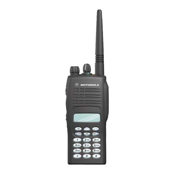
- Page 1 Portable Radios contact control Detailed Service Manual...
-
Page 3: Safety And General Information
Your radio contains a transmitter and a receiver. When it is ON, it receives and transmits radio frequency (RF) energy. Exposure To Radio Frequency Energy Your Motorola Two-Way Radio, is designed to comply with the following National and International Standards and Guidelines regarding exposure of human beings to radio frequency electromagnetic energy (EME): •... - Page 4 To maintain compliance with FCC RF exposure guidelines, if you wear a radio on your body when transmitting, always place the radio in a Motorola supplied or approved clip, holder, holster, case, or body harness. Use of non-Motorola-approved accessories may exceed FCC RF exposure guidelines. If you do not use a body-worn accessory, ensure the antenna is at least one inch (2.5 cm) from your body...
-
Page 5: Safety And General
Safety-iii SAFETY AND GENERAL • Use While Driving Check the laws and regulations on the use of radios in the area where you drive. Always obey them When using your radio while driving, please: • Give full attention to driving and to the road. •... -
Page 6: Intrinsically Safe Radio Information
WARNING: Do not disassemble the FMRC Approved Product unit in any way that exposes the internal electrical circuits of the unit. Radios must ship from the Motorola manufacturing facility with the hazardous atmosphere capability and FM Approval labeling. Radios will not be “upgraded” to this capability and labeled in the field. -
Page 7: Repair Of Fmrc Approved Products
FMRC Approved model. Do Not Substitute Options or Accessories The Motorola communications equipment certified by Factory Mutual is tested as a system and consists of the FM Approved portable, FM Approved battery, and FM Approved accessories or options, or both. - Page 8 Safety-vi This page intentionally left blank.
-
Page 9: Table Of Contents
Table of Contents Chapter 1 Introduction Scope of Manual ......................1-1 Warranty and Service Support..................1-1 1.2.1 Warranty Period........................1-1 1.2.2 Return Instructions ......................1-1 1.2.3 After Warranty Period ......................1-1 Related Documents ...................... 1-2 Technical Support......................1-2 1.4.1 Piece Parts Availability ......................1-2 Radio Model Chart and Specifications................ - Page 10 viii VHF Transmitter ......................2-12 Figure 2-10:VHF Transmitter Block Diagram..............2-12 2.9.1 Power Amplifier........................2-12 2.9.2 Antenna Switch........................2-12 2.9.3 Harmonic Filter ........................2-13 2.9.4 Antenna Matching Network....................2-13 2.9.5 Power Control Integrated Circuit (PCIC)................2-13 2.10 VHF Receiver....................... 2-13 Figure 2-11:VHF Receiver Block Diagram..............
- Page 11 2.18.3 Automatic Gain Control Circuit ..................2-28 2.18.4 Frequency Generation Circuit.................... 2-29 Figure 2-21:800 MHz Frequency Generation Unit Block Diagram........2-29 2.19 Synthesizer ........................2-30 Figure 2-22:800 MHz Synthesizer Block Diagram ............2-30 2.19.1 Voltage Control Oscillator (VCO)..................2-31 Figure 2-23:800 MHz VCO Block Diagram ..............2-31 2.20 Trunked Radio Systems .....................
- Page 12 VHF Troubleshooting Charts ..................3-15 Troubleshooting Flow Chart for Controller ..................3-15 Troubleshooting Flow Chart for Receiver (Sheet 1 of 2) ..............3-16 Troubleshooting Flow Chart for Receiver (Sheet 2 of 2) ..............3-17 Troubleshooting Flow Chart for Transmitter ................... 3-18 Troubleshooting Flow Chart for Synthesizer...................
- Page 13 Figure 4-9:VHF/UHF Complete Controller Schematic Diagram........4-13 Figure 4-10:VHF/UHF Controller ASFIC/ON_OFF Schematic Diagram ......4-14 Figure 4-11: VHF/UHF Controller ASFIC/ON_OFF Schematic Diagram ......4-15 Figure 4-12:VHF/UHF Controller Micro Processor Schematic Diagram ......4-16 Figure 4-13:VHF/UHF Controller Micro Processor Schematic Diagram ......4-17 Figure 4-14:Controller Memory Schematic Diagram............
- Page 14 Figure 4-51:UHF (450-527MHz) Voltage Controlled Oscillator Schematic Diagram ..4-75 Figure 4-52:UHF (450-527MHz) Transmitter Schematic Diagram........4-76 Figure 4-53:UHF (450-527MHz) Voice Storage Schematic Diagram ......4-77 Figure 4-54:VHF (136-174MHz) Main Board Top Side PCB 8486062B09..... 4-83 Figure 4-55:VHF (136-174MHz) Main Board Bottom Side PCB 8486062B09....4-84 Figure 4-56:VHF (136-174MHz) Controls and Switches Schematic Diagram ....
- Page 15 xiii Figure 4-90:Low Band (29.7-42/35-50MHz) Frequency Generation Unit Synthesizer ......................4-135 Figure 4-91:Lowband (29.7-42/35-50MHz) Frequency Generation Unit VCO Diagram........................ 4-136 Figure 4-92:Lowband (29.7-42/35-50MHz) Transmitter Schematic Diagram ....4-137 Figure 4-93:800MHz (806-870MHz) Main Board Top Side PCB 84860641Z02 ... 4-141 Figure 4-94:800MHz (806-870MHz) Main Board Bottom Side PCB 84860641Z02..4-142 Figure 4-95: 800MHz Popular/Preferred (806-870MHz) Main Board Top Side PCB 8480641Z03 (Rev B) ....................
-
Page 17: Chapter 1 Introduction
In instances where the product is covered under a “return for replacement” or “return for repair” warranty, a check of the product should be performed prior to shipping the unit back to Motorola. This is to ensure that the product has been correctly programmed or has not been subjected to damage outside the terms of the warranty. -
Page 18: Related Documents
Motorola. If the part number is appended with an asterisk, the part is serviceable by a Motorola depot only. If a parts list is not included, this generally means that no user-serviceable parts are available for that kit or assembly. -
Page 19: Radio Model Chart And Specifications
7:00 A. M. to 7:00 P. M. (Central Standard Caribbean: Time) 1-847-538-8023 Monday through Friday (Chicago, U. S. A.) Motorola Parts To Order Parts in the United States of Accessories and Aftermarket Division America: (United States and Canada) 1-800-422-4210, or 847-538-8023 Attention: Order Processing 1-800-826-1913, or 410-712-6200 (U. - Page 20 Radio Model Information Table 1-2 Radio Model Number Example: AAH25KC9AA2 and LAH25KDC9AA3 Type Model Freq. Power Physical Channel Feature Model Model Protocol of Unit Series Band Level Packages Spacing Level Revision Package 2.5W No Display Program- Conventional 2F for AA (136- mable 4F for LA...
-
Page 21: Theory Of Operation
Chapter 2 Theory of Operation Introduction This chapter provides a detailed theory of operation for the radio components. Schematic diagrams for the circuits described in the following paragraphs are located in Figures 4-1 through 4-120. Radio Power Distribution A block diagram of the DC power distribution throughout the radio board is shown in Figure 2-1. A 7.5V battery supplies the basic radio power (UNSWB) directly to the electronic on/off control, audio power amplifier, 3.5V regulator, power amplifier automatic level control (ALC), and low battery detect circuit. -
Page 22: Keypad
Table 2-1 VDD Regulator Scheme by Band Band Regulator Scheme Low Band Dual Dual Dual 800 MHz Dual 900 MHz Dual Table 2-2 Radio Jumpers Dual Vdd Single Vdd Jumpers Regulator Regulator Scheme Scheme R401 R402 R403 R404 R405 R = Regulator Jumper Keypad The keypad block diagram is shown in Figure 2-2. -
Page 23: Controller Board
Controller Board The controller board is the central interface between the various radio functions. It is separated into MCU digital and audio/signalling functions as shown in Figure 2-3. External Mod Out Microphone To Synthesizer Internal Microphone 16.8 / 17.0 MHz Reference Clock Audio/Signalling External... -
Page 24: Real Time Clock
2.4.1 Real Time Clock Radios with displays support a real time clock (RTC) module for purposes of message time stamping and time keeping. The RTC module resides in the microcontroller. The clock uses a back-up lithium- Ion battery for operating power when the primary battery is removed. 2.4.2 Circuit Description The RTC module circuit, shown in Figure 2-4, is powered by the MODB/VSTBY pin and PI6/PI7 from... -
Page 25: Audio/Signaling
2.4.1 Audio/Signaling The audio/signalling/filter/companding IC (ASFIC) and the audio power amplifier (Figure 2-3) form the main components of the audio/signalling section of the controller board. Inputs include a 16.8 MHz clock from the synthesizer, recovered audio and squelch, MCU control signals, and external or internal microphones. -
Page 26: Antenna Switch
2.5.2 Antenna Switch The antenna switch circuit consists of two pin diodes (CR101 and CR102), a pi network (C107, L104 and C106), and two current limiting resistors (R101 and R170). In the transmit mode, B+ at PCIC (U102 pin 23) goes low turning on Q111, which applies a B+ bias to the antenna switch circuit to bias the diodes “on”. -
Page 27: Receiver Front-End
Antenna Pin Diode Antenna Varactor Varactor Crystal RFJack Switch Mixer Tuned Filter Tuned Filter Filter Processing Control Voltage First LO from ASFIC from FGU Recovered Audio Demodulator Squelch RSSI Synthesizer 16.8 MHz Reference Clock SPI Bus Second LO VCO Figure 2-6: UHF Receiver Block Diagram 2.6.1 Receiver Front-End The RF signal received by the antenna is applied to a low-pass filter. -
Page 28: Receiver Back-End
The IF signal coming out of the mixer is transferred to the crystal filter (FL301) through a resistor pad and a diplexer (C322 and L310). Matching to the input of the crystal filter is provided by C324 and L311. The crystal filter provides the necessary selectivity and intermodulation protection. 2.6.2 Receiver Back-End The output of crystal filter FL301 is coupled via R351 and C325 to the input of IF amplifier transistor... -
Page 29: Frequency Generation Circuit
compared to normal operation at room temperature. Resistor R300 and Capacitor C397 form an R-C network used to dampen any transient instability while the AGC is turning on. 2.6.4 Frequency Generation Circuit The frequency generation circuit, shown in Figure 2-7, is composed of Fractional-N synthesizer U201 and VCO/Buffer IC U241. -
Page 30: Voltage Control Oscillator (Vco)
2-10 To achieve fast locking for the synthesizer, an internal adapt charge pump provides higher current at U201 (pin 45) to put the synthesizer within lock range. The required frequency is then locked by normal mode charge pump at U201 (pin 47). Both the normal and adapt charge pumps get their supply from the capacitive voltage multiplier made up of C258, C259, C228, triple diode CR201, and level shifters U210 and U211. -
Page 31: Figure 2-9:Uhf Vco Block Diagram
2-11 transmit mode, the audio signal to be frequency modulated onto the carrier is received through U201 (pin 41). When a high impedance is applied to U241 (pin 19), the VCO operates in BATTERY SAVER mode. In this mode, both the receive and transmit oscillators as well as the receive transmit and prescaler buffer are turned off. -
Page 32: Vhf Transmitter
2-12 VHF Transmitter The VHF transmitter consists of the following basic circuits as shown in Figure 2-10. • Power amplifier • Antenna switch/harmonic filter • Antenna matching network • Power control integrated circuit (PCIC) PCIC Antenna Matching Vcontrol Vcontrol Network Power Amplifier (PA) Antenna Switch/ PA Final... - Page 33 2-13 2.9.3 Harmonic Filter The harmonic filter consists of components C3532 to C3536, L3531, and L3532. This network forms a low-pass filter to attenuate harmonic energy of the transmitter to specifications level. The harmonic filter insertion loss is typically less than 1.2dB. 2.9.4 Antenna Matching Network A matching network, made up of L3538 and C3537, is used to match the antenna impedance to the...
-
Page 34: Receiver Front-End
2-14 Antenna Pin Diode Antenna Varactor Varactor Crystal RFJack Switch Mixer Tuned Filter Tuned Filter Filter Control Voltage First LO from ASFIC from FGU Recovered Audio Demodulator Squelch RSSI Synthesizer 16.8 MHz Reference Clock SPI Bus Second LO VCO Figure 2-11: VHF Receiver Block Diagram 2.10.1 Receiver Front-End The RF signal is received by the antenna and applied to a low-pass filter consisting of L3531, L3532,... -
Page 35: Automatic Gain Control (Agc)
2-15 The IF signal coming out of the mixer is transferred to the crystal filter (Y3200) through a resistor pad (R3321 - R3323) and a diplexer (C3320 and L3309). Matching to the input of the crystal filter is provided by C3200 and L3200. The crystal filter provides the necessary selectivity and intermodulation protection. -
Page 36: Frequency Generation Circuit
2-16 pin is limited by resistors R3316, R3313, R3306, and R3324. Feedback capacitor C3326 provides some stability to this high gain stage. An additional gain control circuit is formed by Q3201 and associated components. Resistors R3206 and R3207 are voltage dividers designed to turn on Q3201 at a significantly higher RSSI level than the level required to turn on pin diode control transistor Q3301. -
Page 37: Voltage Control Oscillator (Vco)
2-17 The loop filter, which consist of C3721, C3722, R3721, R3722, and R3723, provides the necessary dc steering voltage for the VCO and determines the amount of noise and spur passing through. In achieving fast locking for the synthesizer, an internal adapt charge pump provides higher current at U3701, pin 45 to put the synthesizer within lock range. -
Page 38: Figure 2-14:Vhf Vco Block Diagram
2-18 During the transmit condition, when PTT is pressed, 3.2 volts is applied to U3801, pin 19. This activates the transmit VCO by enabling the transmit oscillator and the transmit buffer of U3801. The RF signal at U3801, pin 10 is injected into the input of the PA module (U3501, pin16). This RF signal is the TX RF INJECTION. -
Page 39: Low Band Transmitter
2-19 2.13 Low Band Transmitter The low band transmitter consists of the following basic circuits as shown in Figure 2-15. • Power amplifier (PA). • Antenna switch/harmonic filter. • Antenna matching network. • Power control integrated circuit (PCIC). Antenna Switch Bias SPI Bus PCIC Antenna... -
Page 40: Harmonic Filter
2-20 disconnecting the transmitter from the antenna while L103 and C147 form a series resonant circuit effectively connect the receiver to the antenna. 2.13.3 Harmonic Filter The harmonic filter consists of components C103, C106, C103, C107,C110, C111, C114, C115 and inductors L100, L101, and L102 which are a part of the SH100 assembly. -
Page 41: Figure 2-16:Low Band Receiver Block Diagram
2-21 Antenna Lowpass Antenna Highpass Lowpass Crystal RFJack Filter Switch Mixer Filter Filter Filter First LO Processing from FGU Recovered Audio Demodulator Squelch IF IC U303 RSSI Synthesizer 17.0 MHz Reference Clock SPI Bus Second LO VCO Figure 2-16: Low Band Receiver Block Diagram 2.14.1 Receiver Front-End The RF signal received by the antenna is routed through the transmitter lowpass filter and antenna... -
Page 42: Receiver Back-End
2-22 2.14.2 Receiver Back-End The output of crystal filter FL301 is connected to the input of IF amplifier transistor U301. Components L303 and C348 and R301 form the termination for the crystal filter and the signal is coupled to one gate of U301 by C303. -
Page 43: Figure 2-17:Low Band Frequency Generation Unit Block Diagram
2-23 5V signal goes to pins 13 and 30 while the 3.3V signal goes to pins 5, 20, 34 and 36 of U201. The synthesizer in turn generates a superfiltered 4.3V which powers the VCOs and buffers. In addition to the VCO, the synthesizer also interfaces with the logic and ASFIC circuitry. Programming for the synthesizer is accomplished through the data, clock and chip select lines (pins 7, 8 and 9) from the microprocessor, U409. -
Page 44: Figure 2-18:Low Band Synthesizer Block Diagram
2-24 DATA (U409 Pin 100) LOCK LOCK (U409 Pin 56) DATA CLOCK (U409 Pin 1) FREFOUT FREF (U303 Pin 21 & U404 Pin 34) 6,17,22,29,31,33,44 CSX (U409 Pin 2) MOD IN (U404 Pin 40) IOUT MODIN Steering 2-Pole Line 13,30 Loop Filter +5V (U204 Pin 4) IADAPT... -
Page 45: Prescalar Feedback
2-25 rejecting the receive LO injection signals at 139 - 160 MHz. This filter is comprised of L204, L211, L212, C230 and C231. The other filter is a highpass filter which passes 139 - 160 MHz signals for the receive LO into the mixer while rejecting the transmit injection signals at 29.7 -50 MHz. -
Page 46: Antenna Switch
2-26 This RF driver IC is capable of supplying an output power of 0.3W (pin 13 and 14) with an input signal of 2.5mW (4dBm) (pin16). The current drain would typically be 200mA while operating in the frequency range of 806-870MHz. The 85Y73 LDMOS PA is capable of supplying an output power of 4.5W with an input signal of 0.3W. -
Page 47: 800 Mhz Receiver
2-27 2.18 800 MHz Receiver The receiver functions are shown in Figure 2-20 and are described in the paragraphs that follow. Antenna Pin Diode 3-Pole 3-Pole Antenna Ceramic Ceramic Crystal RFJack Switch Block Filter Block Filter Mixer Filter Processing First LO from FGU Recovered Audio Demodulator... -
Page 48: Receiver Back-End
2-28 2.18.2 Receiver Back-End The output of crystal filter FL350 is matched to the input of the dual gate MOSFET IF amplifier transistor U352 by components L355, R359 and C376. Voltage supply to the IF amplifier is taken from the receive 5 volts (R5). AGC voltage is applied to the second gate of U352. The IF amplifier provides a gain of about 11dB. -
Page 49: Figure 2-21:800 Mhz Frequency Generation Unit Block Diagram
2-29 • the slope of the voltage at the output of U302 vs. the strength of the incoming RF at the antenna. As the RF into the antenna increases the following occurs: • The output voltage of the receiver backend inverter U350 decreases. •... -
Page 50: Synthesizer
2-30 Transmit modulation from the ASFIC is supplied to pin10 of U201. Internally the audio is digitized by the Fractional-N and applied to the loop divider to provide the low-port modulation. The audio runs through an internal attenuator for modulation balancing purposes before going out to the VCO. 2.19 Synthesizer The Fractional-N Synthesizer uses a 16.8MHz crystal (FL201) to provide a reference for the system. -
Page 51: Voltage Control Oscillator (Vco)
2-31 2.19.1 Voltage Control Oscillator (VCO) The voltage controlled oscillator block diagram is shown in Figure 2-23. AUX3 (U201 Pin 2) Level Shifter Network AUX4 (U201 Pin 3) TRB_IN Pin 20 Pin 19 Pin 7 Rx-SW TX/RX/BS Pin 13 Switching Network Tx-SW Pin 12 Prescaler Out... -
Page 52: Trunked Radio Systems
2.20.1 Privacy Plus Trunked Systems Privacy Plus is a proprietary trunking protocol developed by Motorola which allows a large number of users to share small amounts of frequencies without interfering with each other. The Privacy Plus configuration consists of shared multiple channel repeaters. The Privacy Plus Trunked system includes a Central Controller, which directs the users to the open channels. -
Page 53: Passport™ Trunked Systems
2-33 for customization for special requirements, and provision made to further standardized features to be added to the protocol in the future. The standard defines only the over-air signalling and imposes only minimum constraints on system design. ™ 2.20.4 PassPort Trunked Systems PassPort is an enhanced trunking protocol developed by Trident Microsystems that supports wide area dispatch networking. -
Page 54: 900 Mhz Transmitter
2-34 2.20.4.5 BackLight Driver and LED's The logic level signal from the radio microcontroller is translated via Q611 and applied to Q610 which uses Switched Battery Voltage (SWB+) to operate the keypad backlight LED’s. 2.20.4.6 Voice Storage The Voice Storage (VS) can be used to store audio signals coming from the receiver or from the microphone. -
Page 55: Power Amplifier
2-35 The 900 MHz transmitter contains the following basic circuits: • power amplifier • antenna switch • harmonic filter • power control integrated circuit (PCIC). 2.21.1 Power Amplifier The power amplifier consists of two devices: • 5185130C65 driver IC (U101) and •... -
Page 56: 900 Mhz Receiver
2-36 2.22 900 MHz Receiver Antenna Pin Diode 3-Pole 3-Pole Antenna Ceramic Ceramic Crystal RFJack Switch Block Filter Block Filter Mixer Filter Processing First LO from FGU Recovered Audio Demodulator Squelch U351 RSSI Synthesizer 16.8 MHz Reference Clock SPI Bus Second LO VCO Figure 2-25: 900 MHz Receiver Block Diagram... -
Page 57: Receiver Back-End
2-37 2.22.2 Receiver Back-End The output of crystal filter FL350 is matched to the input of the dual gate MOSFET IF amplifier transistor U352 by components L355, R359, and C376. Voltage supply to the IF amplifier is taken from the receive 5 volts (R5). AGC voltage is applied to the second gate of U352. The IF amplifier provides a gain of about 11dB. -
Page 58: Automatic Gain Control Circuit
2-38 Table 2-8 Hear Clear Logic and IC Status LO Clamp Disable U851-C2 HCI Disable U851-B6 SWB+ LO Clamp Disable U851-D1 *RX1:receive voice with carrier squelch, PL or DPL (Flutter Fighter can be on or off). **RX2:refers to receive mode with all other data HST/MDC/DTMF (Flutter Fighter must be off). 2.22.3.1 Receive Path for Radios with Hear Clear The audio signal enters Hear Clear controller from DEMOD_OUT signal on DISC. -
Page 59: Frequency Generation Circuitry
2-39 The output of inverter U350 is also used to control the receiver front end AGC. The receiver front end automatic gain control circuit provides and additional 20 dB of gain reduction. The output of the receiver back end inverter U350 is fed into the receiver front end AGC inverter U302. -
Page 60: 900 Mhz Synthesizer
2-40 the microprocessor. A 3.3V dc signal from synthesizer lock detect line indicates to the microprocessor that the synthesizer is locked. Transmit modulation from the ASFIC is supplied to pin10 of U201. Internally the audio is digitized by the Fractional-N and applied to the loop divider to provide the low-port modulation. The audio runs through an internal attenuator for modulation balancing purposes before going out to the VCO. -
Page 61: 900 Mhz Voltage Control Oscillator (Vco)
2-41 2.25 900 MHz Voltage Control Oscillator (VCO) AUX3 (U201 Pin 2) Level Shifter Network AUX4 (U201 Pin 3) TRB_IN Pin 20 Pin 19 Pin 7 Rx-SW TX/RX/BS Pin 13 Switching Network Tx-SW Pin 12 Prescaler Out Presc U201 Pin 32 (U201 Pin 28) Vcc-Superfilter Pin 3... - Page 62 2-42 The operation logic is shown in Table 2-9. Table 2-9 Level Shifter Logic Desired Mode AUX 4 AUX 3 High (@3.2V) High (@4.8V) High Battery Saver Hi-Z/Float (@2.5V) In the receive mode, U250 pin 19 is low or grounded. This activates the receive VCO by enabling the receive oscillator and the receive buffer of U250.
-
Page 63: Chapter 3 Maintenance
Chapter 3 Maintenance Introduction This chapter of the manual describes: • Preventive maintenance • Safe handling of CMOS devices • Repair procedures and techniques Preventive Maintenance The radios do not require a scheduled preventive maintenance program; however, periodic visual inspection and cleaning is recommended. Inspection Check that the external surfaces of the radio are clean, and that all external controls and switches are functional. -
Page 64: Safe Handling Of Cmos And Ldmos
When damaged parts are replaced, identical parts should be used. If the identical replacement component is not locally available, check the parts list for the proper Motorola part number and order the component from the nearest Motorola Communications parts center listed in the “Piece Parts”... - Page 65 • Chip Components Use either the RLN-4062 Hot-Air Repair Station or the Motorola 0180381B45 Repair Station for chip component replacement. When using the 0180381B45 Repair Station, select the TJ-65 mini- thermojet hand piece. On either unit, adjust the temperature control to 700 degrees F. (370 degrees C), and adjust the airflow to a minimum setting.
-
Page 66: Recommended Test Tools
• Remove the circuit board and inspect the repair. No cleaning should be necessary. Recommended Test Tools Table Table 3-1 lists the recommended tools used for maintaining this family of radios. These tools are also available from Motorola. Table 3-1 Recommended Test Tools Motorola Part Number... -
Page 67: Replacing The Circuit Board Fuse
Replacing the Circuit Board Fuse Replacing the Circuit Board Fuse In cases where the radio fails to turn on when power is applied, the circuit board fuse should always be checked as a probable cause of the failure. The locations of the fuse for both the UHF and VHF boards are shown in Figure 3-1. -
Page 68: Figure 3-1:Uhf/Vhf/Low Band/800Mhz/900Mhz Circuit Board Fuse Locations
Replacing the Circuit Board Fuse J102 R328 R340 C307 C108 C339 L303 Q301 C340 R304 C3301 R101 C3231 CR303 C341 L304 C3232 C342 C321 C345 C3233 R305 C311 R347 C3242 C314 C334 C347 P100 C3234 C3224 C356 U301 C348 C395 C132 C312 C3321... -
Page 69: Removing And Reinstalling The Circuit Board
2. Lift the circuit board out of the radio chassis, then remove and discard the thermal pad located between the circuit board and chassis. 3. After repairs, replace the thermal pad (Motorola P/N 7580556Z01) then reinstall the circuit board into the radio chassis. - Page 70 Power Up Self-Test Error Codes If the error code Then, there is To correct the problem ... displayed is ... a ... No Display improperly connected check connection between main board and display display module or module or replace with new display module. damaged display module.
-
Page 71: Uhf Troubleshooting Charts
UHF Troubleshooting Charts UHF Troubleshooting Charts MCU Check Press PTT. Red LED does not Before replacing light up Power Up Not able to pro- MCU, check SPI Alert Tone gram RF Board AUDIO Audio at clock, SPI data, J403 Audio AudioPA and RF IC select at Pin 2 &... -
Page 72: Troubleshooting Flow Chart For Receiver (Sheet 1 Of 2)
3-10 UHF Troubleshooting Charts START Bad SINAD Bad 20dB Quieting No Recovered Audio Audio at pin Check Controller 27 of U301? Induce or inject 1st IF into XTAL Filter IF Freq: 45.1MHz Check Q320 bias circuitry for faults Audio heard? Rotate Freq. -
Page 73: Troubleshooting Flow Chart For Receiver (Sheet 2 Of 2)
UHF Troubleshooting Charts 3-11 Inject RF into J101 Trace IF signal Q302 collec- from L311 to IF Signal tor OK? Q302. Check for at L311? IF signal bad XTAL filter present? Before replacing U301, check U301 voltages; 1st LO O/P trace IF signal RF Signal at Check FGU... -
Page 74: Troubleshooting Flow Chart For Transmitter
3-12 UHF Troubleshooting Charts START No Power Is There B+ Check Q111 Bias for Ant switch Is Control Volt- Check PCIC Is Current age High or Low High Check Drive to Module 1. Check Pin Diodes 2. Check Harmonic Filter Is Drive Troubleshoot Inspect/Repair Tx. -
Page 75: Troubleshooting Flow Chart For Synthesizer
UHF Troubleshooting Charts 3-13 Check U248, 3.3V at U201 Start L201 & L202 pins 5, 20, 34 & 36 Visual Check CR201, Correct check of the U210, U211, C258, Problem Board OK? C259 & C228 Is U201 Pin Is 16.8MHz 16.8MHz at pin 6 of Replace... -
Page 76: Troubleshooting Flow Chart For Vco
3-14 UHF Troubleshooting Charts START Change U241 Change No LO? L253 O/C? L253 Pin 10 TRB = 5V? Tx Carrier? >1V? VCO OK Check R245 for dry joint or faulty AUX 3 Check High? R260 Check U201 Pin 2 for 3.2V Change L243 V ctrl 0V... -
Page 77: Vhf Troubleshooting Charts
VHF Troubleshooting Charts 3-15 VHF Troubleshooting Charts MCU Check Press PTT. Red LED does not Before replacing light up Power Up Not able to pro- MCU, check SPI Alert Tone gram RF Board AUDIO Audio at clock, SPI data, J403 Audio AudioPA and RF IC select at Pin 2 &... -
Page 78: Troubleshooting Flow Chart For Receiver (Sheet 1 Of 2)
3-16 VHF Troubleshooting Charts START Bad SINAD Bad 20dB Quieting No Recovered Audio Audio at pin Check Controller 27 of U3220? Induce or inject 1st IF into XTAL Filter IF Freq: 45.1MHz Check Q3270 bias circuitry for faults. Audio heard? Rotate Freq. -
Page 79: Troubleshooting Flow Chart For Receiver (Sheet 2 Of 2)
VHF Troubleshooting Charts 3-17 Inject RF into J3501 Trace IF signal Q3200 collec- from C3200 to IF Signal at tor OK? Q3200. Check for C3200? IF signal bad XTAL filter. present? Before replacing U3220, check U3220 volt- 1st LO O/P ages;... -
Page 80: Troubleshooting Flow Chart For Transmitter
3-18 VHF Troubleshooting Charts START No Power Is There B+ Check Bias for Ant Q3561 switch Is Control Volt- Is Current Check PCIC age High or Low High Check Drive to Module 1. Check Pin Diodes 2. Check Harmonic Filter Is Drive Troubleshoot Inspect/Repair Tx. -
Page 81: Troubleshooting Flow Chart For Synthesizer
VHF Troubleshooting Charts 3-19 Check U3201, 3.3V at U3701 Start L3731 pins 5, 20, 34 & 36 Visual Check D3701, Correct check of the D3702, U3701, Problem Board OK? C3701 - C3707 Is U3701 Pin 47 Is 16.8MHz 16.8MHz Replace at pin 6 of AT = 13 VDC Signal at... -
Page 82: Troubleshooting Flow Chart For Vco
3-20 VHF Troubleshooting Charts START Change U3801 L3831, L3832, Change L3833 O/ No LO? L3831, L3832 Pin 10 TRB = 3.2V? Tx Carrier? >1V? VCO OK Check R3811, L3811 for dry joint or faulty AUX 3 Check High? R3829 Change Check U3701 L3821, Pin 2 for 3.2V... -
Page 83: Low Band Troubleshooting Charts
Low Band Troubleshooting Charts 3-21 Low Band Troubleshooting Charts MCU Check Press PTT. Red LED does not Before replacing light up Power Up Not able to pro- MCU, check SPI Alert Tone gram RF Board AUDIO Audio at clock, SPI data, J403 Audio AudioPA and RF IC select... -
Page 84: Troubleshooting Flow Chart For Receiver (Sheet 1 Of 2)
3-22 Low Band Troubleshooting Charts START Bad SINAD Bad 20dB Quieting No Recovered Audio Audio at pin Check Controller 27 of U303? Spray of inject 1st IF into XTAL Filter IF Freq: 109.65 MHz Check Q301 bias circuitry for faults. Audio heard? Rotate Freq. -
Page 85: Troubleshooting Flow Chart For Receiver (Sheet 2 Of 2)
Low Band Troubleshooting Charts 3-23 Inject RF into J101 Trace IF signal U301 drain IF Signal at from L301 to L301? U301. Check for IF signal bad XTAL filter present? Before replacing U303, check U303 voltages; 1st LO O/P trace IF signal RF Signal at Check FGU 310OK? -
Page 86: Troubleshooting Flow Chart For Transmitter
3-24 Low Band Troubleshooting Charts START No Power Is control voltage Is Current Check PCIC at U101 Pin 1 > 5 ~ 2 A? Check input to U101, Pin 16 1. Check Pin Diodes 2. Check Harmonic Filter 3. Check PA Bias Troubleshoot Is voltage >... -
Page 87: Troubleshooting Flow Chart For Synthesizer
Low Band Troubleshooting Charts 3-25 Check U200 3.3V at U205 Start and L225 pins 5, 20, 34 & 36 Visual Correct check of the Problem Board OK? Check C247, C249, Is 17.0 MHz 17.0MHz Is U205 Pin Replace C283, C284, C285, Signal at signal at 47 >... -
Page 88: Troubleshooting Flow Chart For Vco
3-26 Low Band Troubleshooting Charts No RX LO or No No TX LO or No signal at U205 Pin signal at U205 Pin 32 in RX 32 in TX Check signal at Check signal at collector of Q201 collector of Q201 Check L204, L211, L212, Level >... -
Page 89: 800 Mhz Troubleshooting Charts
800 MHz Troubleshooting Charts 3-27 800 MHz Troubleshooting Charts MCU Check Press PTT. Red LED does not light Before replacing MCU, Power Up Not able to pro- AUDIO check SPI clock, SPI Audio at Alert Tone gram RF Board data, and RF IC select Audio PA (U420) J403 Audio at input... -
Page 90: Troubleshooting Flow Chart For Receiver (Sheet 1 Of 2)
3-28 800 MHz Troubleshooting Charts START Bad SINAD Bad 20dB Quieting No Recovered Audio Audio at Check Controller pin 27 of U351? Spray or inject 1st IF into XTAL Filter IF Freq: 109.65 MHz Check Q350 bias cir- cuitry for faults Audio heard? Rotate Freq. -
Page 91: Troubleshooting Flow Chart For Receiver (Sheet 2 Of 2)
800 MHz Troubleshooting Charts 3-29 Inject RF into J101 Trace IF signal from Is the level of the L353 to U352. IF signal of the IF Signal at Check for bad XTAL output of U352 as L353? filter. indicated? Before replacing U351, check U351 voltages;... -
Page 92: Troubleshooting Flow Chart For Transmitter
3-30 800 MHz Troubleshooting Charts START Low Power No Power No Power out or Low Power Is overall radio current between 0.8 and 1.3 A when transmit- ting? Is there a Is the fuse short circuit Replace F501 Check L101, L102, C101, F501 OK? after C113? CR101 for open circuit... -
Page 93: Troubleshooting Flow Chart For Synthesizer
800 MHz Troubleshooting Charts 3-31 Check U248 3.3V at U201 Start & L202 pins 5, 20, 34 & 36 Visual Check D201, D202, Correct check of the C244, C245, C246 & Problem Board OK? C247. Is 16.8MHz 16.8MHz Is U201 Pin 47 at pin 6 of Replace Signal at... -
Page 94: Troubleshooting Flow Chart For Vco
3-32 800 MHz Troubleshooting Charts START Is Tx signal Is LO signal VCO is OK. present at the PA present at the driver IC, U101? mixer IC U301? Resolder or Is resonator IC replace U205. U205 soldered Is resonator Resolder or IC U206 sol- replace U206. -
Page 95: Passport Trunking Troubleshooting Chart
PassPort Trunking Troubleshooting Chart 3-33 PassPort Trunking Troubleshooting Chart Start Check Radio Operation on a Non PassPort Zone with a Conventional Personality without the Option Board Enabled Check Radio PassPort Programming using CPS Check Switched Battery and Vdd from Radio on PTCB Check Radio PassPort Programming using CPS Rx Demod... -
Page 96: Keypad Troubleshooting Chart
3-34 Keypad Troubleshooting Chart Keypad Troubleshooting Chart Disconnect and Display reconnect 18-pin flex IF STILL START Disconnect and Keypad reconnect 40-pin flex... -
Page 97: 900 Mhz Troubleshooting Charts
900 MHz Troubleshooting Charts 3-35 3.10 900 MHz Troubleshooting Charts Press PTT. Red LED does not light AUDIO Audio at Audio PA (U420) J403 Audio at input Pin 2 & Pin 3. (C447). PTT U409 Pin Check low? Audio PA (U420). -
Page 98: Troubleshooting Flow Chart For Controller (Sheet 2 Of 2)
3-36 900 MHz Troubleshooting Charts MCU Check. Before replacing MCU, Power Up Not able to pro- check SPI clock, SPI Alert Tone gram RF Board data, and RF IC ICs. select. Replace Speaker. Speaker Check U409 EXTAL= Read Radio OK? Setup. -
Page 99: Troubleshooting Flow Chart For Receiver (Sheet 1 Of 2)
900 MHz Troubleshooting Charts 3-37 START Bad SINAD. Bad 20dB Quieting. No Recovered Audio. Audio at Check Controller. pin 27 of U351? Spray or inject 1st IF into XTAL Filter. IF Freq: 109.65 MHz Check Q350 bias cir- cuitry for faults Audio heard? Rotate Freq. -
Page 100: Troubleshooting Flow Chart For Receiver (Sheet 2 Of 2)
3-38 900 MHz Troubleshooting Charts Inject RF into J101. Trace IF signal from Is the level of the L353 to U352. IF signal of the IF Signal at Check for bad XTAL output of U352 as L353? filter indicated? Before replacing U351, check U351 voltages;... -
Page 101: Troubleshooting Flow Chart For Transmitter
900 MHz Troubleshooting Charts 3-39 START Low Power No Power No Power out or Low Power. Check C163, Is overall radio C127, and Replace current between C142 for open parts. 0.8 and 1.3 A circuit. when transmit- ting? Is there a Is the fuse Replace short circuit... -
Page 102: Troubleshooting Flow Chart For Synthesizer
3-40 900 MHz Troubleshooting Charts START Check U248 3.3V at U201 Start & L202. pins 5, 20, 34 Is Tx signal Is LO signal & 36. VCO is OK. present at the PA present at the driver IC, U101? mixer IC U301? Visual Check D201, D202, Correct... -
Page 103: Schematic Diagrams, Overlays, And Parts Lists
1. Unless otherwise stated, resistances are in Ohms (k = 1000), and capacitances are in picofarads (pF) or microfarads (µF). 2. DC voltages are measured from point indicated to chassis ground using a Motorola DC multime- ter or equivalent. Transmitter measurements should be made with a 1.2 µH choke in series with the voltage probe to prevent circuit loading. -
Page 104: Flex Layout
SIDE 1 LAYER 1 (L1) 6-LAYER CIRCUIT LAYER 2 (L2) BOARD DETAIL VIEWING LAYER 3 (L3) COPPER STEPS IN PROPER INNER LAYERS LAYER 4 (L4) LAYER SEQUENCE LAYER 5 (L5) LAYER 6 (L6) SIDE 2 Flex Layout <- TO KP Front Metal View from Top side TO CTRL ->... -
Page 105: Keypad-Controller Interconnect Flex Schematic
SrD_Snd (DATA) SrD_Snd (DATA) LCD_SEL LCD_SEL SCK_Snd (CLK) SCK_Snd (CLK) VS_RAC VS_RAC FL0830765O Figure 4-2: Keypad-Controller Interconnect Flex Schematic Diagram 4.2.2 Keypad-Controller Interconnect Flex Parts List Reference Motorola Part Description Symbol J100 0980521Z01 Connector, 40 pin J200 0905505Y04 Speaker, 20 ohm... -
Page 106: Universal Flex Connector
4.2.3 Universal Flex Connector J403 J416 J415 J414 J413 J412 J411 J410 J409 J408 J407 J406 J405 J404 Back Metal Front Metal View From Top Side View From Top Side Figure 4-3:Universal Flex Connector... -
Page 107: Universal Connector Flex Schematic
RX_AUDIO/TX_AUDIO BOOT_CTRL J415 BOOT_CTRL J416 M401 C402 100pF Figure 4-4: Universal Flex Connector Schematic Diagram 4.2.5 Universal Flex Connector Parts List Reference Motorola Part No. Description Symbol C402 2113740A55 Cap, 100pF M400 5085962A02 Speaker, 20 ohm M401 5013920A04 Microphone for 5000 and 7000 Series... -
Page 108: Keypad Top And Bottom Overlays
4.2.6 Keypad Top and Bottom Overlays Top View Bottom View Figure 4-5: Keypad Top and Bottom Board Overlays... - Page 109 Bottom View Figure 4-5: Keypad Top and Bottom Board Overlays *FMR-2016A-1* FMR-2016A-1 © 2002 by Motorola, Inc. Commercial, Government and Industrial Solutions Sector 4-2-02 8000 W. Sunrise Blvd., Ft. Lauderdale, FL 33322 Printed in U. S. A. 4/02. All Rights Reserved.