Table of Contents
Advertisement
Quick Links
Advertisement
Table of Contents

Related Manuals for Icom IC-F7000


Summary of Contents for Icom IC-F7000
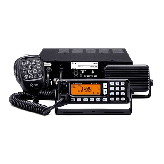
- Page 1 SERVICE MANUAL HF TRANSCEIVER iF7000...
- Page 2 Addresses are provided on the inside back cover for your convenience. Icom, Icom Inc. and are registered trademarks of Icom Incorporated (Japan) in the United States, the United Kingdom, Germany, France, Spain, ussia and/or other countries. NEVER connect the transceiver to an AC outlet or to a DC power supply that uses more than 16 V.
-
Page 3: Table Of Contents
MECHANICAL PARTS AND DISASSEMBLY 7 - 1 RC-26... 7 - 1 7 - 2 HM-146 ... 7 - 1 7 - 3 IC-F7000 ... 7 - 1 SECTION 8 SEMI-CONDUCTOR INFORMATION SECTION 9 BOARD LAYOUTS 9 - 1 HM-146 ...9 - 1... - Page 4 SECTION 1 SPECIFICATIONS • IC-F7000 ‘ ‘ GENERAL • Frequency coverage • Mode • Antenna impedance • Frequency stability • Power supply requirement • Current drain (at 13.8 V DC) • Usable temperature range • Dimensions (projections not included) • Weight ‘...
- Page 5 • RC-26 REMOTE CONTROLLER ‘ ‘ GENERAL • Microphone impedance • Audio output power • Audio output impedance • Usable temperature range • Dimension (projections not included) • Weight • SP-25 EXTERNAL SPEAKER ‘ ‘ GENERAL • Impedance • Input power •...
- Page 6 11 32 287.8 (11 7 16 240 (9 Unit: mm (inch) 1 - 3...
- Page 7 13 16 173.2 (6 29 32 150 (5 7 32 158.2 (6 9 16 25 32 9 16 40 (1 45 (1 40 (1 66.3 (2 1 - 4 51.2 (2 40 (1 6.5 ( Unit: mm (inch) 5.5 ( 15 32 37 (1 Unit: mm (inch)
- Page 8 SECTION 2 INSIDE VIEWS • RC-26 (IC8201: HD64F2134AF20) (IC8201: (IC8201: HD64F2134AF20) HD64F2134AF20) +8V regulator +8V regulator (IC8310: TA78L08F) (IC8310: TA78L08F) (IC8310: +10V regulator +10V regulator (IC8301: AN8009M) (IC8301: (IC8301: AN8009M) AN8009M) Dimmer controller Dimmer controller Dimmer controller (IC8280: TS522ID) (IC8280: (IC8280: TS522ID) DISPLAY BOARD DISPLA...
- Page 9 • IC-F7000 (TOP VIEW) YGR amplifier YGR amplifier YGR amplifier (IC1: PC2709T) (IC1: PC2709T) MAIN UNIT MAIN UNIT MAIN UNIT DSP BO DSP BOARD DSP BOARD RF 3rd mix RF 3rd mixer RF 3rd mixer (IC501: TA4107F) (IC501: TA4107F) TX 3rd mix...
- Page 10 SECTION 3 ABOUT EXTERNAL REFERENCE SIGNAL INPUT ‘ ‘ IN CASE OF USING EXTERNAL REFERENCE SIGNAL NEED TO MODIFY the PLL unit (bottom side) as below when using external reference. q Remove R5251 from the PLL unit. w Solder disconnect points (CP5041) on the PLL unit. R5251 CP5041 3 - 1...
- Page 11 Unsolder connect points (CP5041) on the PLL unit. w Solder R5251 to the original position, or solder disconnect points (CP5251) on the PLL unit. ‘ ‘ CONNECTION Connect the external reference oscillator to the IC-F7000 as below. IC-F7000 front panel CP5251...
-
Page 12: Receiver Circuits
SECTION 4 CIRCUIT DESCRIPTION 4-1 RECEIVER CIRCUITS 4-1-1 RF FILTER CIRCUIT (PLL AND MAIN UNITS) Received signals from the antenna connector are applied to the transmit/receive switching and protection relay (PLL unit; RL7301) which is controlled by the CPU via the “TRXS” line. The signals pass through the 30 MHz cut-off low-pass filter (PLL unit;... - Page 13 4-1-5 DSP RECEIVER CIRCUIT (MAIN AND DSP UNITS) The DSP (Digital Signal Processor) circuit enables digital IF filter, digital noise reduction, digital PSN (Pulse Shift Network), phase demodulation, digital automatic notch, and etc. The 3rd IF signal is applied to the IF amplifier (MAIN unit; IC1002, pin 5) after being passed through the low-pass filter (MAIN unit;...
-
Page 14: Transmitter Circuits
4-2 TRANSMITTER CIRCUITS 4-2-1 MICROPHONE AMPLIFIER CIRCUIT (RC-26, MAIN AND DSP UNITS) The microphone amplifier circuit amplifies microphone audio signal to a level needed for the DSP circuit. Audio signals from the [MIC] connector (J8701, pin 6) are amplified at the AF amplifier (IC8280, pin 3), and then applied to the gate modulator IC (MAIN unit;... - Page 15 4-2-5 RF CIRCUIT (MAIN, PA, PLL UNITS AND DRI- VER BOARD) The RF circuit amplifies operating (transmitting) frequency to obtain 100 W (125 W: 1.6–4 MHz for [OTH]) of RF output. The RF signals from the 1st mixer circuit pass through the low-pass filter (L702, L703, C706, C707, C709–C711, C721), and are then applied to the RF amplifier (Q701).
-
Page 16: Pll Circuits
4-2-6 ALC CIRCUIT (PLL AND MAIN UNITS) The ALC (Automatic Level Control) circuit controls the gain of IF amplifiers in order for the transceiver to output a con- stant RF power even when the supplied voltage shifts, etc. The RF power level is detected at the power detector circuit (PLL unit;... - Page 17 The AF signals from the microphone are amplified at the AF amplifier (IC8280) via the “MIC” signal. The signals are applied to the IC-F7000’s main unit through the J2501, pin 1 via the “FMOD” line. 4-4-3 KEY’S BACK LIGHTS CIRCUIT (DISPLAY BOARD) The key”s back lights compose of DS8305, DS8306,...
-
Page 18: Power Supply Circuits
4-5 POWER SUPPLY CIRCUITS 4-5-1 PA UNIT VOLTAGE LINE LINE DESCRIPTION HV13 The voltage from an external power supply. The same voltage as the HV13 line passed through the fuse (F6701). The same voltage as the HV13 line passes S13V through the switching relay (RL6701). -
Page 19: Port Allocations
4-6 PORT ALLOCATIONS 4-6-1 MAIN CPU (MAIN UNIT; IC3303) Port Description number name Outputs T8 regulator circuit (MAIN unit; Q1501) control signal. Outputs R8 and R13V regulator cir- cuits (MAIN unit; Q1502, Q1505) con- trol signal. Outputs serial strobe signal to the PSEL latch control IC (IC3601, pin 1). - Page 20 4-6-4 OUTPUT EXPANDER IC FOR BANDPASS FIL- TERS (MAIN UNIT; IC3604) Port Description number name Outputs 0.5–1.999999 MHz bandpass filter control signal. Outputs 2–2.999999 MHz bandpass filter control signal. Outputs 3–4.999999 MHz bandpass filter control singnal. Outputs 5–6.999999 MHz bandpass filter control signal.
- Page 21 4-6-7 FRONT CPU PORT ALLOCATIONS (RC-26, DISPLAY BOARD; IC8201) Port Description number name 15–17 Outputs LCD drive signals. Input port for the [CALL] switch. CALK Low: [CALL] switch is pushed. Input port for the [∫] switch. Low: [∫] switch is pushed. Input port for the [√] switch.
- Page 22 SECTION 5 ADJUSTMENT PROCEDURES 5-1 PREPARATION When adjusting the contents on page 5-9, a JIG CABLE (see illustration as below) is required. Some adjustments must be performed on the “ADJUSTMENT MODE”. Entering the “ADJUSTMENT MODE”, refer to the next page in detail. REQUIRED TEST EQUIPMENT EQUIPMENT GRADE AND RANGE...
- Page 23 ENTERING THE ADJUSTMENT MODE 1 Turn the power OFF. 2 Push and hold the HM-146’s [CALL] and RC-26’s [EMG] switches, then turn the power ON. [CALL] OPERATING ON THE ADJUSTMENT MODE • Enter the TX adjustment from the MAIN menu. •...
- Page 24 5-2 PLL UNIT ADJUSTMENT ADJUSTMENT ADJUSTMENT CONDITIONS LPL LOCK • Operating frequency : 0.5000 MHz VOLTAGE • Mode • Receiving • Operating frequency : 0.4999 MHz • Receiving HPL LOCK • Operating frequency : 29.9999 MHz VOLTAGE • Mode • Receiving •...
- Page 25 • IC-F7000 BOTTOM VIEW • PLL UNIT TOP VIEW R5255 L5203 L5204 Reference frequency adjustment P5201 Reference frequency ckeck point PLL unit C5521 HPL lock voltage adjustment CP5402 HPL lock voltage ckeck point CP5302 LPL lock voltage ckeck point L5305...
- Page 26 5-3 PA AND FILTER UNITS ADJUSTMENT ADJUSTMENT ADJUSTMENT CONDITIONS IDLING • Operating frequency : 12.2350 MHz CURRENT • Mode (For drive • Apply no audio signal to the [MIC] con- FETs) nector. • Disconnect J6702. • Preset R6304 and R6412 on the PA unit to max.
- Page 27 R6412 Idling current adjustment (For final transistors) R6304 Idling current adjustment (For drive FETs) • PLL UNIT BOTTOM VIEW • IC-F7000 BOTTOM VIEW CP7331 (REF line) SWR detector check point CP7332 (FOR line) Connect to ground C7275 SWR detector adjustment...
- Page 28 5-4 RECEIVER ADJUSTMENTS ”TOTAL GAIN”, “S-METER” and “DSC PEAK” adjustments must be performed at “ADJUSTMENT MODE”. ADJUSTMENT ADJUSTMENT CONDITIONS NOISE NULL • Operating frequency : 0.5 MHz POINT • Mode • Preset L209 parallel to top edge of its chassis. •...
- Page 29 Preset to top edge of its chassis L209 PRESETTING Set to same height here. • RC-26 FRONT PANEL L401 L403 L801 L404 L405 • IC-F7000 BOTTOM VIEW [OK] 5 - 8 R217 R218 Noise null point adjustment L207 L208 L211...
- Page 30 5-5 TRANSMITTER ADJUSTMENTS The following adjustments must be performed at “ADJUSTMENT MODE” after “SWR DETECTOR” and “RECEIVER” ADJUST- MENTS in the SECTION 5-3 and 5-4. ADJUSTMENT ADJUSTMENT CONDITIONS TRANSMIT • While pushing HM-146’s [CALL] PEAK AND switch and RX-26’s [EMG] switch, turn TOTAL GAIN power ON.
- Page 31 Connect an ammeter : J3E panel (50 A) between an external power supply : 1.5 kHz and the transceiver. : 100 mV • IC-F7000 BOTTOM VIEW [OK] 5 - 10 ADJUSTMENT VALUE UNIT ADJUST 24.0 A [AUS] R6516 28.0 A [OTH]...
-
Page 32: Ic-F7000
SECTION 6 PARTS LIST 6-1 IC-F7000 [MAIN UNIT] ORDER DESCRIPTION 1110004080 S.IC µPC2709T-E3 IC101 1130011640 S.IC IS62C1024L-45T <ACE> IC301 1110004080 S.IC µPC2709T-E3 IC501 1110005460 S.IC TA4107F (TE12L) IC901 1110005460 S.IC TA4107F (TE12L) IC1001 1130006220 S.IC TC4W53FU (TE12L) IC1002 1110005450 S.IC... - Page 33 [MAIN BOARD] ORDER DESCRIPTION 6200010670 S.COIL C2520C-R18G (0.18U) 6200010740 S.COIL C2520C-R27G-A 6200002860 S.COIL NL 252018T-4R7J 6200002040 S.COIL NL 252018T-101J 6180003440 COIL ELEAH 4R7JA 6200005010 S.COIL NL 252018T-100J 6180003460 COIL ELEAH 3R9JA 6200002040 S.COIL NL 252018T-101J 6200002040 S.COIL NL 252018T-101J 6200002040 S.COIL NL 252018T-101J 6200005490...
- Page 34 [MAIN UNIT] ORDER DESCRIPTION R109 7030003370 S.RESISTOR ERJ3GEYJ 271 V (270 R110 7030003370 S.RESISTOR ERJ3GEYJ 271 V (270 R111 7030003370 S.RESISTOR ERJ3GEYJ 271 V (270 R112 7030003370 S.RESISTOR ERJ3GEYJ 271 V (270 R113 7030003370 S.RESISTOR ERJ3GEYJ 271 V (270 R114 7030003280 S.RESISTOR ERJ3GEYJ 470 V (47...
- Page 35 [MAIN UNIT] ORDER DESCRIPTION R1208 7030003610 S.RESISTOR ERJ3GEYJ 273 V (27 k ) R1209 7030003640 S.RESISTOR ERJ3GEYJ 473 V (47 k ) R1210 7030009591 S.RESISTOR ERA3YED 472V R1211 7030005871 S.RESISTOR ERA3YKD 104V (100 k ) R1212 7030003740 S.RESISTOR ERJ3GEYJ 334 V (330 k ) R1213 7030005871 S.RESISTOR...
- Page 36 [MAIN UNIT] ORDER DESCRIPTION R3332 7030003640 S.RESISTOR ERJ3GEYJ 473 V (47 k ) R3333 7030003360 S.RESISTOR ERJ3GEYJ 221 V (220 R3334 7030003640 S.RESISTOR ERJ3GEYJ 473 V (47 k ) R3335 7030003360 S.RESISTOR ERJ3GEYJ 221 V (220 R3336 7030003360 S.RESISTOR ERJ3GEYJ 221 V (220 R3337 7030003360 S.RESISTOR...
- Page 37 [MAIN UNIT] ORDER DESCRIPTION C171 4030011280 S.CERAMIC C1608 CH 1H 271J-T C172 4030011600 S.CERAMIC C1608 JB 1E 104K-T C173 4030007160 S.CERAMIC C1608 CH 1H 181J-T C174 4030011600 S.CERAMIC C1608 JB 1E 104K-T C175 4030007040 S.CERAMIC C1608 CH 1H 180J-T C176 4030011600 S.CERAMIC C1608 JB 1E 104K-T...
- Page 38 [MAIN UNIT] ORDER DESCRIPTION C1002 4030011600 S.CERAMIC C1608 JB 1E 104K-T C1003 4030011600 S.CERAMIC C1608 JB 1E 104K-T C1004 4030018610 S.CERAMIC C1608 CH 1H 182J-T C1005 4030017800 S.CERAMIC C1608 CH 1H 561J-T C1006 4030006880 S.CERAMIC C1608 JB 1H 472K-T C1007 4030006880 S.CERAMIC C1608 JB 1H 472K-T...
- Page 39 [MAIN UNIT] ORDER DESCRIPTION 6510007020 CONNECTOR TMP-J01X-V6 6510007020 CONNECTOR TMP-J01X-V6 J301 6510007020 CONNECTOR TMP-J01X-V6 J601 6510007020 CONNECTOR TMP-J01X-V6 J1101 6510021650 CONNECTOR IMSA-9180B-30B J1102 6510022810 CONNECTOR IMSA-9180B-22B J1451 6450000102 CONNECTOR HSJ1857-01-1220 J1801 6510023840 CONNECTOR TCS5107-182011 J1901 6510021720 S.CONNECTOR 30FLT-SM1-TB J2051 6510023050 CONNECTOR TCS7286-01-241 J3001...
- Page 40 [PLL UNIT] ORDER DESCRIPTION R5088 7030003640 S.RESISTOR ERJ3GEYJ 473 V (47 k ) R5089 7030009620 S.RESISTOR ERJ12YJ120U (12 R5090 7030003520 S.RESISTOR ERJ3GEYJ 472 V (4.7 k ) R5091 7030003520 S.RESISTOR ERJ3GEYJ 472 V (4.7 k ) R5092 7030003520 S.RESISTOR ERJ3GEYJ 472 V (4.7 k ) R5093 7030003640 S.RESISTOR...
- Page 41 [PLL UNIT] ORDER DESCRIPTION C5080 4030006880 S.CERAMIC C1608 JB 1H 472K-T C5081 4030006880 S.CERAMIC C1608 JB 1H 472K-T C5082 4030006880 S.CERAMIC C1608 JB 1H 472K-T C5083 4030006900 S.CERAMIC C1608 JB 1H 103K-T C5084 4030006900 S.CERAMIC C1608 JB 1H 103K-T C5085 4030008680 S.CERAMIC C2012 JF 1C 105Z-T...
- Page 42 [PLL UNIT] ORDER DESCRIPTION C7126 4010005360 CERAMIC HM11SJ SL 301J 500V C7128 4010005370 CERAMIC HM11SJ SL 331J 500V C7129 4010005870 CERAMIC HM95SJ SL 221J 500V C7130 4030011550 S.CERAMIC GRM31M2C2H680JV01L (GRM42-6 CH) C7131 4030012480 S.CERAMIC GRM31M2C2H121JV01L (GRM42-6 CH) C7132 4030012480 S.CERAMIC GRM31M2C2H121JV01L (GRM42-6 CH) C7133 4030006880...
- Page 43 [PA UNIT] ORDER DESCRIPTION R6406 7030010260 S.RESISTOR ERJ1TYJ 3R3 U R6407 7030001010 S.RESISTOR MCR50JZHJ 10 R6408 7030001010 S.RESISTOR MCR50JZHJ 10 R6409 7070001180 RESISTOR ERX2SJ 2R7 (2.7 R6410 7070001180 RESISTOR ERX2SJ 2R7 (2.7 R6411 7070000521 RESISTOR ERX3SJ 2R7 (2.7 R6412 7310004710 TRIMMER EVM-2AGA00 B23 (202) R6413...
- Page 44 [DSP BOARD] ORDER DESCRIPTION IC9701 1110001900 S.IC µPC4570G2-T1 IC9801 1130010560 S.IC SN74AHC244PWR Q9021 1530002060 S.TRANSISTOR 2SC4081 T106 R Q9201 1590001660 S.TRANSISTOR XP4312 (TX) Q9301 1590000430 S.TRANSISTOR DTC144EUA T106 Q9302 1590000430 S.TRANSISTOR DTC144EUA T106 D9301 1750000370 S.DIODE DA221 TL D9302 1750000370 S.DIODE DA221 TL D9303...
- Page 45 [DSP BOARD] ORDER DESCRIPTION C9303 4030011600 S.CERAMIC C1608 JB 1E 104K-T C9304 4030006880 S.CERAMIC C1608 JB 1H 472K-T C9305 4030011600 S.CERAMIC C1608 JB 1E 104K-T C9306 4030011600 S.CERAMIC C1608 JB 1E 104K-T C9307 4030011600 S.CERAMIC C1608 JB 1E 104K-T C9308 4030011600 S.CERAMIC C1608 JB 1E 104K-T...
-
Page 46: Front Unit
6-2 RC-26 [FRONT UNIT] ORDER DESCRIPTION W8001 8900009230 CABLE OPC-908 (P=1 N=10 L=60) W8002 8900012650 CABLE OPC-1272 TYX4003-210100 W8005 8900008860 CABLE OPC-875 (N:20 L:70) [DISPLAY BOARD] ORDER DESCRIPTION IC8201 1140011600 S.IC HD64F2134AFA20 (EX-2621A) IC8202 1110005770 S.IC S-80942CNMC-G9C-T2 IC8205 1130009700 S.IC LC73872M-TRM IC8250 1130005720 S.IC... -
Page 47: Connect Board
[DISPLAY BOARD] ORDER DESCRIPTION C8311 4030011600 S.CERAMIC C1608 JB 1E 104K-T C8312 4030011600 S.CERAMIC C1608 JB 1E 104K-T C8313 4510004640 S.ELECTROLYTIC ECEV1CA470SP J8201 6510021260 S.CONNECTOR B9B-ZR-SM3-TF J8202 6510022620 S.CONNECTOR 10FMN-BMTTR-A-TBT J8205 6510022540 S.CONNECTOR 20FMN-BMTTR-A-TBT J8701 6450001470 CONNECTOR 95003-2881 J8702 6510022620 S.CONNECTOR 10FMN-BMTTR-A-TBT DS8300 5040002470... - Page 48 6-3 HM-146 [MAIN UNIT] ORDER DESCRIPTION 1130008990 S.IC LC7366NM-TRM <KN> 1590003340 S.TRANSISTOR DTA114EUA T106 <KN> 1730002500 S.ZENER MA8062-M (TX) <KN> 6060000700 S.CERAMIC PRBC 3.58AR <KN> 6200008620 S.COIL LK1608-R82K-T <KN> 7030009370 S.RESISTOR MCR03EZHJ 220 7030009360 S.RESISTOR MCR03EZHJ 100 7030009410 S.RESISTOR MCR03EZHJ 2.2 k — (222) <KN> 7030009450 S.RESISTOR MCR03EZHJ 5.6 k —...
- Page 49 Screw PH B0 3 MP26 8850001610 Spring washer M4 SUS MP28 8930052390 1743 SW rubber MP29 8930054170 2129 sheet [MIC UNIT] REF. QTY. 7-3 IC-F7000 [CHASSIS PARTS] 8 NI-ZU REF. 6 ZK J4501 8 NI-ZU W4501 W4502 MP4501 MP4502 MP4503 MP4504 QTY.
- Page 50 MUTE CALL MP4014 (F) W4001 (F) MP4019 (F) F4002 (F) F4001 (F) MP8108 (R) MP8109 (R) J4002 (F) EP4002 (F) MP8107 (R) (R): RC-26 (F): IC-F7000 [ACCESSRIES] • IC-F7000 QTY. REF. ORDER MC4001 0800007310 SP4001 0800007490 J4002 6450001280 P4001 5610000340...
-
Page 51: Rear Board
REAR BOARD J8701 (D) MP8015 (F) MP8002 (F) MP8023 (F) DS8920 (C) MP8001 (F) 7 - 3 MP8018 (F) to IC-F7000 MAIN unit J2051 to HM-146 MIC unit W1 MP8013 (F) MP8012 (F) W8002 (F) DISPLAY BOARD MP8006 (F) Unit abbreviations... - Page 52 MP4530 (C) MP4512 (C) EP1451 (M) MP4501 (C) MP4531 (C) MP4529 (C) MP4528 (C) MP4503 (C) MP4513 (C) MP4511 (C) IC-F7000 MP4513 (C) to RC-26 FRONT parts W8002 MP4502 (C) MP4520 (C) J5051 (P) J4501 (C) MP4504 (C) J5041 (P)
- Page 53 SECTION 8 SEMI-CONDUCTOR INFORMATION • TRANSISTOR AND FET’S 2SA1037AK S 2SA1586 GR 2SB1201 S (Symbol: FS) (Symbol: SG) (Symbol: B1201) 2SC4116 GR 2SC4213 B 2SC4215 O (Symbol: LG) (Symbol: AB) (Symbol: QO) 2SD1619 T TD 2SD1664 T100Q 2SD1801 S TL (Symbol: DB) (Symbol: DAQ) (Symbol: CE)
- Page 54 SECTION 9 BOARD LAYOUTS 9-1 HM-146 • TOP VIEW LOCK 9 - 1 9-2 RC-26 9-2-1 CONNECT BOARD • TOP VIEW 9-2-2 REAR BOARD • TOP VIEW to RC-26 DISPLAY board J8701 J8802 to DISPLAY board J8702...
- Page 55 • BOTTOM VIEW (CONNECT BOARD) J8920 to DISPLAY board J8205 • BOTTOM VIEW (REAR BOARD) • BOTTOM VIEW (MIC UNIT) TUNE SCAN MUTE CALL 9 - 2...
- Page 56 9-2-3 DISPLAY BOARD • TOP VIEW J8701 to HM-146 MIC unit J1 9 - 3 MUTE TUNE SCAN CALL...
- Page 57 • BOTTOM VIEW (DISPLAY BOARD) J8205 J8202 to IC-F7000 MAIN unit J2051 J8201 to CONNECT board J8920 9 - 4 J8702 to REAR board J8802...
-
Page 58: Ic-F7000
9-3 IC-F7000 9-3-1 DSP BOARD • TOP VIEW 9 - 5... - Page 59 • BOTTOM VIEW (DSP BOARD) MAIN unit J1102 J9901 DSPI1 DSPI1 DSPI2 DSPI2 AGC2 AGC1 AGC2 AGC1 DSPO1 DSPO1 DSPO2 DSPO2 to MAIN unit J1102 J9902 DRES DSKY GND1 VSQL ALE2 CWST GND1 OBSY GND1 GND1 CK_IN to MAIN unit J1101 9 - 6 MAIN unit J1101 GND1...
- Page 60 9-3-2 MAIN UNIT • TOP VIEW J1102 DSPO2 DSPO1 AGC2 AGC1 DSPI2 DSPI1 to DSP board J9901 CONTROLLER 8 7 4 6 J2051 EXT SP to SP-25 to RC-26 DISPLAY boad J8201 9 - 7 J1901 J3602 J3601 2 1 3 to PLL unit J5001 to PLL unit J7331 W7321...
- Page 61 • BOTTOM VIEW (MAIN UNIT) 9 - 8...
-
Page 62: Pa Unit
9-3-3 PA UNIT • TOP VIEW to CHASSIS W4501 to TUNER J6703 W7001 FLIN from PLL unit J7001 9 - 9 to MAIN unit J1901 J6701 J6412 VARISTOR-2 board J6501 to FAN J6301 to DRIVER DRVI board DRVI from/to MAIN unit J1 J6302 J6411 DRVO... - Page 63 • BOTTOM VIEW (PA UNIT) 9 - 10...
-
Page 64: Pll Unit
9-3-4 PLL UNIT • TOP VIEW W4503 from CHASSIS unit J4501 J7331 to MAIN unit J3602 9 - 11 W7001 FLIN to PA unit J6401 REMOTE J5001 J5081 to MAIN unit J3601 20 W5601 to MAIN unit J601 J5051 EXT REF M1Lo AF/MOD... - Page 65 • BOTTOM VIEW (PLL UNIT) 9 - 12...
-
Page 66: Driver Board
9-3-5 DRIVER BOARD • TOP VIEW 9-3-6 VARISTOR-1 BOARD 9 - 13 VARI VARO... -
Page 67: Varistor-2 Board
• BOTTOM VIEW (DRIVER BOARD) to PA unit J6302 9-3-7 VARISTOR-2 BOARD to PA unit J6301 9 - 14 VARO... -
Page 68: Block Diagram
IC3603 TD62783AF BU4094BCF BUFF DECI X3301 CR-636A 14.7456MHz VSQL EEPROM IC3301 H13V CAT24WC256K1.8 H13V MMOD IC-F7000 RC-26 Explanatory notes VOLTAGE LINE TX LINE RX LINE COMMON LINE Bus LINE 64.455MHz Q201 Q202 BW=15kHz Q204 Q205 MMBFU310 4 0.5-2MHz FI201 33MHz 1.6MHz... -
Page 69: Wiring Diagram
FAFG FMODG FMOD J8702 J8205 J8920 CHASSIS W8005 AFIN AFIN AFIN F13H F13H DISPLAY BOARD CONNECT BOARD 11 - 1 IC-F7000 Explanatory notes TX LINE RX LINE COMMON LINE HM-146 RC-26 HEADPHONE /CLONE J8801 J8802 AFIN AFIN AFIN F13H F13H... -
Page 70: Voltage Diagrams
ERJ3GE-JPW R8242 R8241 MESUREMENT CONDITIONS frequency:13.8 MHz mode:J3E(USB) ANT(RX):no input (TX):no modulation Digital tester unit:V FH13 range:20V input impedance:10M to IC-F7000 MAIN (3) unit J2051 Explanatory notes VOLTAGE LINE TX LINE RX LINE J8920 LRES LDB0 LDB1 LDB2 LDB3 LDB4... -
Page 71: Ic-F7000
12-2 IC-F7000 12-2-1 MAIN UNIT (1) MAIN UNIT (1) J301 M2Lo from PLL unit J5201 RX: 5.03V J601 from PLL 1LoB unit J5601 0.18 0.27 to PA PC2709T unit J6702 1SV307 0.0022 0.012 0.0022 from PLL unit J7321 2SC4213 Explanatory notes... -
Page 72: Main Unit (2)
12-2-2 MAIN UNIT (2) MAIN UNIT (2) BUS LINE1 D119 1SV307 C182 L152 LR-440 D120 C178 L148 Q102 1SV307 LR-439 2SC5551 R117 2.7k C181 L153 LR-440 Q101 XP4311 Q103 2SC5551 R118 R120 2.7k R131 ERJ3GE-JPW S13V Q105 R128 R129 DTC114EU PRES R13V R13V... - Page 73 12-2-3 MAIN UNIT (3) MAIN UNIT (3) BUS LINE1 S13V S13V HV13 HV13 R3021 PWRS R3017 R3003 RXS1 R3004 TXS1 SQLC R3006 SQLC1 RFML R3007 RFML1 R3008 DCV1 NSEN R3009 NSEN1 TEMP R3010 TEMP1 ASEN R3011 ASEN1 BEEP R3012 BEEP1 D3031 R3034 MA2S111...
-
Page 74: Pa Unit
12-2-4 PA UNIT J6302 C6851 0.01 DRVO DRVO Q6851 PD55015 R6852 DRIVER BOARD J6301 DRVI DRVI C6105 R6107 Q6101 R6101 L6101 C6103 J6702 RD01MUS1 0.22 from MAIN unit J1 TX: 2.54V C6715 0.047 J6703 D6703 L6706 HF70ACC635050-T MA2S111 13.8 L6705 HF70ACC635050-T TUM4 L6707... -
Page 75: Pll Unit (1)
12-2-5 PLL UNIT (1) PLL UNIT (1) RL7031 MZ-9D-K L7036 LR-236 L7035 C7034 470p C7035 390p RL7061 MZ-9D-K L7067 LR-236 L7065 C7080 82p C7081 68p RL7091 MZ-9D-K L7096 LR-263 L7095 C7106 82p C7107 68p RL7121 MZ-9D-K L7127 LR-241 L7125 C7126 300p C7110 10p J7001 P7001... -
Page 76: Pll Unit (2)
12-2-6 PLL UNIT (2) PLL UNIT (2) Explanatory notes VOLTAGE LINE L5202 7.76V R5203 7.20V C5206 0.5p Q5202 2SC4215 L5203 L5204 LS-471A LS-471A R5207 C5202 0.001 6.91V Q5281 2SC4215 C5282 0.001 (32MHz) R5041 EXT REF C5262 R5256 C5263 X5251 CR-770 C5261 L5255 L5254... -
Page 77: Dsp Board
12-2-7 DSP BOARD DSP BOARD C9005 0.0047 L9001 L9005 IC9005 SN74AHC2G08HDCT IC9001 SN74AHC74PW C9001 C9004 0.0047 0.0047 IC9003 SN74AHC74PW IC9001 IC9001 IC9003 SN74AHC74PW SN74AHC74PW SN74AHC74PW 1.3V 1.0V R9015 L9015 C9016 R9016 IC9015 ERJ3GE-JPW 0.0047 TC7SZU04FU C9015 0.0047 77ns 1.7V 1.5V L9051 C9051 0.0047... - Page 79 S-14012HZ-C1 1-1-32, Kamiminami, Hirano-ku, Osaka 547-0003, Japan C 2003 Icom Inc.