Table of Contents
Advertisement
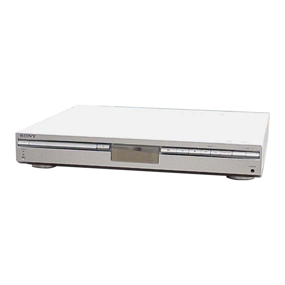
HCD-SB100/SB200
SERVICE MANUAL
Ver. 1.4 2005.04
• HCD-SB100/SB200 are the amplifier, DVD/CD and
tuner section in DAV-SB100/SB200.
Manufactured under license from Dolby Laboratories. "Dolby", "Pro Logic",
and the double-D symbol are trademarks of Dolby Laboratories.
Confidential Unpublished works. Copyright 1992-1997 Dolby
Laboratories. All rights reserved.
Manufactured under license from Digital Theater Systems, Inc.
US Pat. No. 5,451,942 5,956,674, 5,974,380, 5,978,762 and other
worldwide patents issued and pending. "DTS" and "DTS Digital Surround"
are registered trademarks of Digital Theater Systems, Inc. Copyright 1996,
2000 Digital Theater Systems, Inc. All rights reserved.
Sony Corporation
9-879-182-05
Audio Group
2005D16-1
Published by Sony Engineering Corporation
© 2005.04
Photo: HCD-SB100
SPECIFICATIONS
(SB100: US, CND models)
Power supply
120V AC, 60Hz
Power consumption
70W, No more than 1 W (120V AC) (at the power saving mode)
Mass
4.7
kg
External dimensions (W x H x D) 430 x 70 x 383.5 mm
Operating conditions
Temperature: 5°C to 35°C, Operation status: Horizontal
Operating humidity
5% to 85%
Laser
Semiconductor laser, wavelength 650 nm for VCD and DVD,
wavelength 780 nm for CD
Emission duration
Continuous
Signal system
NTSC 525/60
Frequency response (audio)
2 Hz ~ 20 kHz (±1.0 dB)
Signal-to-noise ratio (audio)
More than 75 dB (1 kHz, NOP, 20 kHz LPF/A-Filter)
Dynamic range (audio)
More than 70 dB
Harmonic distortion (audio)
0.5 % (1 kHz, at 12W position) (20 kHz LPF/A-Filter)
Inputs
VIDEO
(AUDIO IN):
Sensitivity: 800 m V
Impedance: 50 kilohms
1.0 V (p-p), 75 Ω, negative sync., RCA jack
Video output
S VIDEO OUT
(Y) 1.0 V (p-p), 75 ohms, negative sync, Mini DIN 4-pin x 1
(C) 0.286 V (p-p) 75 ohms
COMPONENT VIDEO OUT
(Y) 1.0 V (p-p), 75 ohms, negative sync, RCA jack x 1
(P
/C
)/(P
B
B
Tuning Range
87.5 - 108 MHz
Intermediate Frequency
10.7 MHz
Signal-to Noise Ratio
60 dB (Mono)
Tuning Range
522 - 1,611 kHz
Intermediate Frequency
450 kHz
50W + 50W (8 Ω at 1 kHz, THD 10 %)
Stereo mode
Surround mode
Front: 50W + 50W
(* Depending on the sound mode
Centre*: 50W
settings and the source, there
Surround*: 50W + 50W (8Ω at 1 kHz, THD 10 %)
may be no sound output.)
Subwoofer*: 80W (4Ω at 50 Hz, THD 10 %)
PHONES: (32 Ω, 25mW)
Outputs
/C
) 0.7 V (p-p), 75 ohms, RCA jack x 2
R
R
US Model
Canadian Model
HCD-SB100
AEP Model
UK Model
E Model
Australian Model
HCD-SB100/SB200
• Abbreviation
AUS : Australian model
CND : Canadian model
EA
: Saudi Arabia model
EE
: East European model
RU
: Russian model
SP
: Singapore model
– Continued on next page –
DVD RECEIVER
Advertisement
Table of Contents

Related Manuals for Sony HCD-SB100


Summary of Contents for Sony HCD-SB100
-
Page 1: Service Manual
UK Model E Model Australian Model HCD-SB100/SB200 Photo: HCD-SB100 • HCD-SB100/SB200 are the amplifier, DVD/CD and tuner section in DAV-SB100/SB200. Manufactured under license from Dolby Laboratories. “Dolby”, “Pro Logic”, • Abbreviation and the double-D symbol are trademarks of Dolby Laboratories. - Page 2 HCD-SB100/SB200 Ver. 1.1 (SB100: AEP, UK, RU, EE models) (SB100: EA, SP, AUS models) Power supply 220-240V AC, 50/60Hz Power supply 220-240V AC, 50/60Hz Power consumption 70W, No more than 1 W (220-240V AC) (at the power saving mode) Power consumption...
- Page 3 THE PARTS LIST ARE CRITICAL TO SAFE OPERATION. FONCTIONNEMENT. NE REMPLACER CES COM- POSANTS REPLACE THESE COMPONENTS WITH SONY PARTS WHOSE QUE PAR DES PIÈCES SONY DONT LES NUMÉROS SONT PART NUMBERS APPEAR AS SHOWN IN THIS MANUAL OR DONNÉS DANS CE MANUEL OU DANS LES SUPPLÉMENTS IN SUPPLEMENTS PUBLISHED BY SONY.
-
Page 4: Table Of Contents
HCD-SB100/SB200 Ver. 1.1 TABLE OF CONTENTS SERVICING NOTES 7-4. Printed Wiring Board ..........5 – AMP Section SB200 (Component Side) – ....51 7-5. Printed Wiring Board GENERAL ..............6 – AMP Section SB200 (Conductor Side) – ..... 52 7-6. Schematic Diagram – AMP Section (1/6) – ....53 DISASSEMBLY 7-7. -
Page 5: Servicing Notes
HCD-SB100/SB200 Ver. 1.1 SECTION 1 SERVICING NOTES NOTES ON HANDLING THE OPTICAL PICK-UP BLOCK OR BASE UNIT The laser diode in the optical pick-up block may suffer electrostatic break-down because of the potential difference generated by the charged electrostatic load, etc. on clothing and the human body. -
Page 6: General
HCD-SB100/SB200 SECTION 2 GENERAL This section is extracted from instruction manual. • Abbreviation : Australian model : Canadian model : Saudi Arabia model : East European model : Russian model : Singapore model Front Panel Controls VOLUME Control @ / 1 (POWER) indicator Press “+”... -
Page 7: Rear Panel Connections
HCD-SB100/SB200 (SB100: AEP, UK, RU, EE models) Rear Panel Connections AC Power Cord Plug into the power source. EURO AV OUTPUT (TO TV) Connect to your TV set. MONITOR OUT (VIDEO) Connect to a TV with video input. VIDEO (AUDIO IN L/R) Connect the audio output of an external source (VCR, LD player, etc). - Page 8 HCD-SB100/SB200 (SB100: US, CND, EA, SP, AUS models) Rear Panel Connections AC Power Cord Plug into the power source. SPEAKER CONNECTORS Connect the six supplied MONITOR OUT (VIDEO) speakers to these terminals. Connect to a TV with video input. VIDEO (AUDIO IN L/R) Connect the audio output of an external source (VCR, LD player, etc).
- Page 9 HCD-SB100/SB200 (SB200: AEP, UK, RU, EE models) Rear Panel Connections AC Power Cord Plug into the power source. EURO AV OUTPUT (TO TV) Connect to your TV set. MONITOR OUT (VIDEO) Connect to a TV with video input. VIDEO (AUDIO IN R/L) Connect the audio output of an external source (VCR, LD player, etc).
- Page 10 HCD-SB100/SB200 (SB200: SP, AUS models) Rear Panel Connections AC Power Cord Plug into the power source. SPEAKER CONNECTORS Connect the six supplied MONITOR OUT (VIDEO) speakers to these terminals. Connect to a TV with video input. VIDEO (AUDIO IN L/R) Connect the audio output of an external source (VCR, LD player, etc).
-
Page 11: Remote Control
HCD-SB100/SB200 Remote Control SLEEP SONY TV DIRECT To place the unit in the Sleep mode. Select the output source to DVD directly. TUNER/BAND TV @ / 1 Selects the DVD Receiver’s tuner as the Switches TV ON and OFF. listening choice. (FM and AM bands) -
Page 12: Disassembly
HCD-SB100/SB200 Ver. 1.1 SECTION 3 DISASSEMBLY • This set can be disassembled in the order shown below. • : In order to remove set AMP board please remove POWER board and DVD board. 3-1. DISASSEMBLY FLOW 3-2. CASE (Page 13) 3-3. -
Page 13: Case
HCD-SB100/SB200 Ver. 1.1 • Follow the disassembly procedure in the numerical order given. 3-2. CASE 3 two screws 2 two case screws 1 two case screws 4 case 3-3. FRONT PANEL ASSY SECTION 3 five claws 1 w ire (flat type) -
Page 14: Power Board
HCD-SB100/SB200 Ver. 1.1 3-4. POWER BOARD 5 connector 4 connector (CN902) (CN901) 1 connector (CN903) 3 four screws 2 connector (PN901) 6 POWER board... -
Page 15: Dvd Board
HCD-SB100/SB200 Ver. 1.1 3-5. DVD BOARD 1 two screws 2 cover 3 w ire (flat type) 23p (PDM01) 4 w ire (flat type) 11p (PDM02) 5 connector (CN903) 6 four screws 8 connector (PDA03) 9 DVD board 7 connector (PDA02) -
Page 16: Dvd Mechanism Deck
HCD-SB100/SB200 Ver. 1.1 3-6. DVD MECHANISM DECK 1 two screws 2 cover 7 DVD mechanism deck 3 w ire (flat type) 23p (PDM01) 6 screw 4 w ire (flat type) 8 two claws 11p (PDM02) 9 door DVD 5 screw 3-7. -
Page 17: Amp Board
HCD-SB100/SB200 Ver. 1.1 3-8. AMP BOARD 1 w ire (flat type) 12p (PN103) 2 two screws 3 two screws 7 AMP board 4 two screws 5 screw 6 two screws... -
Page 18: Electrical Trouble Shooting Guide
HCD-SB100/SB200 Ver. 1.1 SECTION 4 ELECTRICAL TROUBLE SHOOTING GUIDE 4-1. AUDIO PART 1. POWER CHECK FLOW INSERT POWER CORD. TURN ON CHECK POWER PLUG THE RED LED? AND POWER SUPPLY CIRCUIT . TURN POWER ON. IS POWER ON? CHECK POWER SUPPLY CIRCUIT. - Page 19 HCD-SB100/SB200 Ver. 1.1 2. AUDIO µ.COM CIRCUIT POWER ON Does other function Does CD/DVD name appear at FLD? appear at FLD? Does it appear Does LOADING DVD Error at appear at FLD? FLD? Check Does no Dise or Connector(PN902)if Reconnet it.
- Page 20 HCD-SB100/SB200 Ver. 1.1 3. FRONT CIRCUIT (1/2)
- Page 21 HCD-SB100/SB200 Ver. 1.1 4. FRONT CIRCUIT (2/2)
- Page 22 HCD-SB100/SB200 Ver. 1.1 4-2. DVD PART 1. POWER CHECK FLOW Does other function name at FLD? PDM02 PDM01 PDA02 PDA03 PDA01...
- Page 23 HCD-SB100/SB200 Ver. 1.1 2. TEST & DEBUG FLOW...
- Page 24 HCD-SB100/SB200 Ver. 1.1...
- Page 25 HCD-SB100/SB200 Ver. 1.1...
- Page 26 HCD-SB100/SB200 Ver. 1.1...
- Page 27 HCD-SB100/SB200 Ver. 1.1...
- Page 28 HCD-SB100/SB200 Ver. 1.1...
- Page 29 HCD-SB100/SB200 Ver. 1.1 4-3. DETAILS AND WAVEFORMS ON SYSTEM TEST AND DEBUGGING 1. SYSTEM 27MHz CLOCK, RESET, FLASH R/W SIGNAL 1) MT1379 main clock is at 27MHz (X501) 2) MT1336 reset is high active...
- Page 30 HCD-SB100/SB200 Ver. 1.1 3) RS232 waveform during procedure (Downloading) 4) Flash R/W enable signal during download (Downloading)
- Page 31 HCD-SB100/SB200 Ver. 1.1 2. SDRAM CLOCK 1) MT1379 main clock is at 27MHz (X501) 3. TRAY OPEN/CLOSE SIGNAL 1) Tray open/close waveform...
- Page 32 HCD-SB100/SB200 Ver. 1.1 2) Tray close waveform 3) Tray open waveform...
- Page 33 HCD-SB100/SB200 Ver. 1.1 4. SLED CONTROL RELATED SIGNAL (NO DISC CONDITION) 5. LENS CONTROL RELATED SIGNAL (NO DISC CONDITION)
- Page 34 HCD-SB100/SB200 Ver. 1.1 6. LASER POWER CONTROL RELATED SIGNAL (NO DISC CONDITION) 7. DISC TYPE JUDGEMENT WAVEFORM...
- Page 35 HCD-SB100/SB200 Ver. 1.1...
- Page 36 HCD-SB100/SB200 Ver. 1.1 8. FOCUS ON WAVEFORM...
- Page 37 HCD-SB100/SB200 Ver. 1.1 9. SPINDLE CONTROL WAVEFORM (NO DISC CONDITION)
- Page 38 HCD-SB100/SB200 Ver. 1.1 10. TRACKING CONTROL RELATED SIGNAL (SYSTEM CHECKING)
- Page 39 HCD-SB100/SB200 Ver. 1.1 11. RF WAVEFORM 12. MT1379 AUDIO OPTICAL AND COAXIAL OUTPUT (ASPDIF)
- Page 40 HCD-SB100/SB200 Ver. 1.1 13. MT1379 VIDEO OUTPUT WAVEFORM 1) Full colorbar signal (CVBS) 2) Y...
- Page 41 HCD-SB100/SB200 Ver. 1.1 3) C 14. AUDIO OUTPUT FORM AUDIO DAC 1) Audio related Signal...
-
Page 42: Test Mode
HCD-SB100/SB200 Ver. 1.1 SECTION 5 TEST MODE DVD Processor Reset Procedure: 1. Press the DVD SETUP key on the remote commander to enter the set up screen. The following SET UP menu is dis- played. 2. Move the cursor to [TV Aspect,16:9 Wide] on the screen. -
Page 43: Electrical Adjustment
HCD-SB100/SB200 Ver. 1.2 SECTION 6 ELECTRICAL ADJUSTMENT [RFMON Level Check] DVD SECTION Connection: [TEST DISC LIST] oscilloscope Use the following test disc on test mode. DVD board TDV-520CSO (DVD-SL): PART No. J-2501-236-A LUV-P01 (CD): PART No. 4-999-032-01 PDM01 pin 2 (RFOUT) –... - Page 44 HCD-SB100/SB200 Ver. 1.1 MEMO...
-
Page 45: Diagrams
HCD-SB100/SB200 Ver. 1.1 SECTION 7 DIAGRAMS • Circuit Boards Location THIS NOTE IS COMMON FOR PRINTED WIRING BOARDS AND SCHEMATIC DIAGRAMS. (In addition to this, the necessary note is printed in each block.) For Schematic Diagrams. For Printed Wiring Boards. -
Page 46: Block Diagram - Dvd Section
HCD-SB100/SB200 Ver. 1.1 7-1. BLOCK DIAGRAM – DVD SECTION – IC201 OPTICAL CD/DVD RF AMP, PICK-UP SERVO CONTROL UNIT 96 DVDRFIP RF OUT PROG L IC5C1 DVD VIDEO IC501 Q501 DVDC MPEG & VIDEO PROCESS DRIVE JK601 DVDB RFOP RFIP... -
Page 47: Audio Section
HCD-SB100/SB200 Ver. 1.1 – AUDIO SECTION – IC301 IC502 DIGITAL AUDIO PROCESSOR H.P AMP JK002 PWM HP LP A+INPUT Q503,509 A OUTPUT MUTE A-INPUT PWM HP LN 45 PHONES PWM HP RP B+INPUT R-CH B OUTPUT R-CH PWM HP PN... -
Page 48: Power Section
HCD-SB100/SB200 Ver. 1.1 – POWER SECTION – PN103 IC101 (3/3) L-OUT RMC001 AUDIO TU L SYSTEM CONTROLLER SECTION R-OUT REMOTE R-CH REMOCON CONTROL RECEIVER STEREO STEREO LD001 T902 BD901 TUNER T_CE T CE TRANSFORMER T_RDS_DATA STBY LED STANDBY AC IN... -
Page 49: Printed Wiring Board - Amp Section Sb100 (Component Side)
HCD-SB100/SB200 Ver. 1.1 • See page 45 for Circuit Boards Location. 7-2. PRINTED WIRING BOARD – AMP SECTION SB100 (COMPONENT SIDE) – [AMP BOARD](COMPONENT SIDE) (SB100) IC601 IC202 IC501 IC710 IC750 IC770 IC730 IC502 IC101 IC301 • Semiconductor Location Ref. No. -
Page 50: Printed Wiring Board - Amp Section Sb100 (Conductor Side)
HCD-SB100/SB200 Ver. 1.1 • See page 45 for Circuit Boards Location. 7-3. PRINTED WIRING BOARD – AMP SECTION SB100 (CONDUCTOR SIDE) – [AMP BOARD](CONDUCTOR SIDE) AEP, UK, RU, EE EURO AV (SB100) JK700 JK602 (TO TV) JK601 SPEAKER OUT PUT... -
Page 51: Printed Wiring Board - Amp Section Sb200 (Component Side)
HCD-SB100/SB200 Ver. 1.1 • See page 45 for Circuit Boards Location. 7-4. PRINTED WIRING BOARD – AMP SECTION SB200 (COMPONENT SIDE) – [AMP BOARD](COMPONENT SIDE) (SB200) IC601 IC202 IC501 IC710 IC750 IC770 IC730 IC502 IC101 • Semiconductor Location IC301 Ref. No. -
Page 52: Printed Wiring Board - Amp Section Sb200 (Conductor Side)
HCD-SB100/SB200 Ver. 1.1 • See page 45 for Circuit Boards Location. 7-5. PRINTED WIRING BOARD – AMP SECTION SB200 (CONDUCTOR SIDE) – [AMP BOARD](CONDUCTOR SIDE) AEP, UK, RU, EE (SB200) EURO AV JK700 JK701 JK602 (TO TV) JK601 SPEAKER SUB WOOFER... -
Page 53: Schematic Diagram - Amp Section (1/6)
HCD-SB100/SB200 Ver. 1.1 • See page 69 for Waveform. • See page 73 for IC Pin Function Description. 7-6. SCHEMATIC DIAGRAM – AMP SECTION (1/6) – AMP BOARD(4/6) DSP SECTION AMP BOARD(5/6) AMP BOARD(5/6) AMP BOARD(3/6) AMP BOARD (1/6) MICOM SECTION... -
Page 54: Schematic Diagram - Amp Section (2/6)
HCD-SB100/SB200 Ver. 1.1 • See page 70 for IC Block Diagrams. 7-7. SCHEMATIC DIAGRAM – AMP SECTION (2/6) – AMP BOARD (2/6) I/O SECTION SB200 * R660,661 R667 100:47 US,CND,SP,EA,AUS IC502 200:9.1 H.P AMP (COMPONENT OPTION) SB200 Q503,504,609 MUTE Q503... -
Page 55: Schematic Diagram - Amp Section (3/6)
HCD-SB100/SB200 Ver. 1.1 • See page 70 for IC Block Diagram. • See page 69 for Waveform. • See page 75 for IC Pin Function Description. 7-8. SCHEMATIC DIAGRAM – AMP SECTION (3/6) – AMP BOARD(1/6) AMP BOARD(1/6,6/6) AMP BOARD... -
Page 56: Schematic Diagram - Amp Section (4/6) (Sb100)
HCD-SB100/SB200 Ver. 1.1 7-9. SCHEMATIC DIAGRAM – AMP SECTION (4/6) (SB100) – HCD-SB100/SB200... -
Page 57: Schematic Diagram - Amp Section (5/6) (Sb200)
HCD-SB100/SB200 Ver. 1.1 7-10. SCHEMATIC DIAGRAM – AMP SECTION (5/6) (SB200) – AMP BOARD(3/6) AMP BOARD(1/6) SMPS AMP BOARD (5/6) (SB200) AMP SECTION IC710 IC730 IC750 IC770 AUDIO POWER DRIVE AUDIO POWER DRIVE AUDIO POWER DRIVE AUDIO POWER DRIVE STA508 STM... -
Page 58: Schematic Diagram - Amp Section (6/6)
HCD-SB100/SB200 Ver. 1.1 7-11. SCHEMATIC DIAGRAM – AMP SECTION (6/6) – AMP BOARD (6/6) SMPS SECTION KTA1281Y -36.1 -28.7 Q971,975 -29.2 -28V REG KTC3205 -29.2 -29.2 -28.7 POWER BOARD (1/2)(SB100) CN901 (Page 67) (100:+32VF)(200:+35V) (100:+32VF)(200:+35V) (100:+32VF)(200:+35V) POWER BOARD -23.6 -23.7... -
Page 59: Printed Wiring Board - Dvd Section
HCD-SB100/SB200 Ver. 1.1 • See page 45 for Circuit Boards Location. 7-12. PRINTED WIRING BOARD – DVD SECTION – [DVD BOARD](CONDUCTOR SIDE) [DVD BOARD](COMPONENT SIDE) AMP BOARD (SB100) AMP BOARD PN200 (SB100) (Page 50) PN201 (Page 50) AMP BOARD AMP BOARD... -
Page 60: Schematic Diagram - Dvd Section (1/3)
HCD-SB100/SB200 Ver. 1.1 • See page 72 for IC Block Diagram. • See page 69 for Waveforms. 7-13. SCHEMATIC DIAGRAM – DVD SECTION (1/3) – DVD BOARD (1/3) DVD SECTION BOARD (3/3) IC501 MPEG&VIDEO PROCESS IC501 MT1379EEC BOARD (2/3) IC5C1... -
Page 61: Schematic Diagram - Dvd Section (2/3)
HCD-SB100/SB200 Ver. 1.1 • See page 71 for IC Block Diagram. • See page 69 for Waveforms. 7-14. SCHEMATIC DIAGRAM – DVD SECTION (2/3) – DVD BOARD (2/3) DVD SECTION INVERTER SWITCH SWITCH IC201 CD/DVD RF AMP SERVO CONTROL IC201... -
Page 62: Schematic Diagram - Dvd Section (3/3)
HCD-SB100/SB200 Ver. 1.1 7-15. SCHEMATIC DIAGRAM – DVD SECTION (3/3) – DVD BOARD (3/3) DVD SECTION POWER BOARD (1/2)(SB100) CN903 (Page 67) POWER BOARD (2/2)(SB200) CN903 (Page 68) BOARD (1/3) AMP BOARD (3/6) PN201 (Page 55) BOARD (1/3) AMP BOARD... -
Page 63: Printed Wiring Board - Front Section
HCD-SB100/SB200 Ver. 1.1 • See page 45 for Circuit Boards Location. 7-16. PRINTED WIRING BOARD – FRONT SECTION – [FRONT BOARD] [LED BOARD] (COMPONENT SIDE) (COMPONENT SIDE) [EAR PHONE BOARD] (COMPONENT SIDE) AMP BOARD (SB200) PN101 (Page 51) [FRONT BOARD]... -
Page 64: Schematic Diagram - Front Section
HCD-SB100/SB200 Ver. 1.1 7-17. SCHEMATIC DIAGRAM – FRONT SECTION – FRONT BOARD (FLUORESCENT INDICATOR TUBE) LED BOARD RMC001 REMOTE CONTROL RECEIVER DRIVER AMP BOARD (1/6) PN102 (Page 53) STAND SW010 PRESET AMP BOARD (1/6) PN101 (Page 53) EAR PHONE BOARD... -
Page 65: Printed Wiring Board - Power Section (Sb100)
HCD-SB100/SB200 Ver. 1.1 • See page 45 for Circuit Boards Location. 7-18. PRINTED WIRING BOARD – POWER SECTION (SB100) – AMP BOARD AMP BOARD (SB100) (SB100) PN901 PN902 [POWER BOARD] (SB100) (Page 50) (Page 50) IC922 IC924 AC IN IC921... -
Page 66: Printed Wiring Board - Power Section (Sb200)
HCD-SB100/SB200 Ver. 1.1 • See page 45 for Circuit Boards Location. 7-19. PRINTED WIRING BOARD – POWER SECTION (SB200) – AMP BOARD AMP BOARD (SB200) (SB200) PN901 PN902 (Page 52) (Page 52) [POWER BOARD] (SB200) AC IN IC922 IC924 IC921... -
Page 67: Schematic Diagram - Power Section (1/2) (Sb100)
HCD-SB100/SB200 Ver. 1.1 7-20. SCHEMATIC DIAGRAM – POWER SECTION (1/2) (SB100) – POWER BOARD (1/2) (SB100) IC921 +5V REG T901 TRANSFORMER IC922 IC924 +12V REG +8V REG BOARD (6/6) PN902 13.6 (Page 58) IC923 +3.3V REG VOLTAGE CONTROLLER 21.4 21.9 -12.7... -
Page 68: Schematic Diagram - Power Section (2/2) (Sb200)
HCD-SB100/SB200 Ver. 1.1 7-21. SCHEMATIC DIAGRAM – POWER SECTION (2/2) (SB200) – POWER BOARD (2/2) (SB200) IC924 IC921 +8V REG +5V REG T901 TRANSFORMER KA378R05 AMP BOARD IC922 (6/6) +12V REG PN902 (Page58) KIA7808 KA78R12 KA78R33 IC923 IC901 VOLTAGE +3.3V REG... - Page 69 HCD-SB100/SB200 Ver. 1.1 • Waveforms – DVD Board – – AMP Board – IC201 oh (DVD RFIP) IC5C1 wa (Y out) IC301 ih (CLK_IN) 1.3 Vp-p 4.5 Vp-p 81 ns 1.1 Vp-p 500 mV/DIV, 20 µ s/DIV 200 mV/DIV, 100 ns/DIV...
-
Page 70: Ic Block Diagrams
HCD-SB100/SB200 Ver. 1.1 • IC Block Diagrams – AMP Board – IC202 CS5331A Comparator Voltage Reference High Digital Decimation Pass SDATA AINL Filter LP Filter Filter SCLK Serial Output Interface AGND LRCK Comparator High Digital Decimation Pass MCLK AINR Filter... - Page 71 HCD-SB100/SB200 Ver. 1.1 – DVD Board – IC202 L6560-A-TE Thermal Shutdown Signal System GND S-GND (LOAD output voltage setting) VCONT BTL-AMP Output VCC2 MUTE MUTE ON/OFF VLO- VIN4 VLO+ VIN4- V04+ VIN4+ VO4- VREF-IN VO3+ VIN1(VREF)-SW VIN1/VREF-SW VO3- VREF- OUT(CH1)
- Page 72 HCD-SB100/SB200 Ver. 1.1 IC5C1 MM1623XFBE S-DC OUT VCC1 VCC2 S1/S2 150kΩ BIAS 200Ω C IN S-DC OUT 75Ω MUTE 1 C OUT DRIVER -6dB 6.75MHz CLAMP CVBS IN YC MIX CLAMP 75Ω Y IN CVBS OUT DRIVER 6.75MHz GND1 GND2 75Ω...
- Page 73 HCD-SB100/SB200 Ver. 1.1 • IC Pin Function Description AMP BOARD IC101 LC87684C-54C7 (SYSTEM CONTROLLER) Pin No. Pin Name Description DVD_RESET Reset signal output to DVD P_CTL Power control signal output DVD_CE CE signal to DVD /STEREO Stereo signal output from the tuner...
- Page 74 HCD-SB100/SB200 Ver. 1.1 Pin No. Pin Name Description VDD4 — Power suply terminal(+5V) 9818_PDN PDN signal output to the Audio Dac 9818_RESET Reset signal output to the Audio Dac NC75 — Not used NC76 — Not used 16:9/4:3 Output signal of TV MODE change...
- Page 75 HCD-SB100/SB200 Ver. 1.1 AMP BOARD IC301 PS9818 (DIGITAL AUDIO PROCESSOR) Pin No. Pin Name Description IO_VSS1 — I/O digital ground. PLL_DVSS — PLL digital ground. PLL_DVDD — PLL peripheral digital power supply. 2.5V supply voltage. PLL_XPD Internal PLL Power Down. Active Low.
- Page 76 HCD-SB100/SB200 Ver. 1.1 Pin No. Pin Name Description PWM3_M Negative PWM output of channel 3. PWM3_ Positive PWM output of channel 3. IO_VDD56 — 3.3V Digital power supply. I/O power supply. IO_VSS57 — I/O digital ground. PWM4_M Negative PWM output of channel 4.
-
Page 77: Exploded Views
HCD-SB100/SB200 SECTION 8 EXPLODED VIEWS NOTE: • -XX and -X mean standardized parts, so they • Abbreviation The components identified by mark 0 or may have some difference from the original : Australian model dotted line with mark 0 are critical for safety. -
Page 78: Chassis Section
HCD-SB100/SB200 Ver. 1.2 8-2. CHASSIS SECTION supplied DVD mechanism section supplied supplied supplied supplied Ref. No. Part No. Description Remark Ref. No. Part No. Description Remark 9-885-069-27 DOOR DVD 9-885-069-49 DVD BOARD ASSY (US,CND) 9-885-071-11 AMP BOARD ASSY (200:UK,AEP,EE) 9-885-069-47 DVD BOARD ASSY (AUS) -
Page 79: Dvd Mechanism Section
HCD-SB100/SB200 Ver. 1.4 8-3. DVD MECHANISM SECTION supplied 106 107 supplied supplied Ref. No. Part No. Description Remark Ref. No. Part No. Description Remark 9-885-072-02 CLAMP ASSEMBLY 9-885-072-25 CAP 9-885-072-04 BASE ASSEMBLY 9-885-072-26 CAP 9-885-072-33 SCREW, DRAWING 9-885-072-30 SHAFT 9-885-072-03 BASE ASSEMBLY... -
Page 80: Electrical Parts List
HCD-SB100/SB200 Ver. 1.4 SECTION 9 ELECTRICAL PARTS LIST NOTE: • Due to standardization, replacements in the • CAPACITORS When indicating parts by reference number, uF: µF parts list may be different from the parts please include the board name. specified in the diagrams or the components •... - Page 81 HCD-SB100/SB200 Ver. 1.3 Ref. No. Part No. Description Remark Ref. No. Part No. Description Remark < CONNECTOR > 9-885-069-32 DVD BOARD ASSY(UK,AEP) 9-885-069-39 DVD BOARD ASSY(EA) PN101 9-885-055-76 CONNECTOR (CIRC),FFC/FPC 9-885-069-49 DVD BOARD ASSY(US,CND) PN102 9-885-074-00 CONNECTOR (CIRC),FFC/FPC 24P 9-885-069-47 DVD BOARD ASSY(AUS)
- Page 82 HCD-SB100/SB200 Ver. 1.4 EAR PHONE FRONT POWER Ref. No. Part No. Description Remark Ref. No. Part No. Description Remark EAR PHONE BOARD 0 C954 9-885-073-80 CAPACITOR HI-VOL 470P/1K **************** 0 CM901 9-885-073-81 CAPACITOR DRAWING 435D < JACK > 0 CM902...
- Page 83 HCD-SB100/SB200 Ver. 1.1 POWER Ref. No. Part No. Description Remark < SENSOR > 0 PC910 8-749-018-95 SENSOR LTV-817B,PHOTO COUPLER(LITEON) 0 PC911 8-749-018-95 SENSOR LTV-817B,PHOTO COUPLER(LITEON) 0 PC912 8-749-018-95 SENSOR LTV-817B,PHOTO COUPLER(LITEON) < CONECTOR > PN901 9-885-073-70 CONNECTOR(CIRC),DRAWING 3P < TRANSISTOR >...
-
Page 84: Revision History
HCD-SB100/SB200 REVISION HISTORY Clicking the version allows you to jump to the revised page. Also, clicking the version at the upper right on the revised page allows you to jump to the next revised page. Ver. Date Description of Revision 2004.09...