Table of Contents
Advertisement
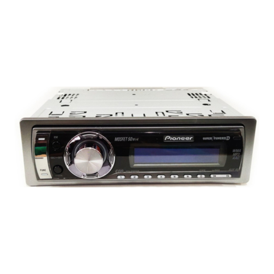
CD RECEIVER
DEH-P590IB
DEH-P5900IB
This service manual should be used together with the following manual(s):
Model No.
Order No.
CX-3195
CRT3815
For details, refer to "Important Check Points for Good Servicing".
PIONEER CORPORATION
PIONEER ELECTRONICS (USA) INC. P.O. Box 1760, Long Beach, CA 90801-1760, U.S.A.
PIONEER EUROPE NV Haven 1087, Keetberglaan 1, 9120 Melsele, Belgium
PIONEER ELECTRONICS ASIACENTRE PTE. LTD. 253 Alexandra Road, #04-01, Singapore 159936
PIONEER CORPORATION 2006
Mech.Module
S10.5COMP2
CD Mech. Module : Circuit Descriptions, Mech. Descriptions, Disassembly
4-1, Meguro 1-chome, Meguro-ku, Tokyo 153-8654, Japan
DEH-P590IB/XN/UC
/XN/UC
Remarks
ORDER NO.
CRT3851
/XN/UC
K-ZZU. DEC. 2006 Printed in Japan
Advertisement
Table of Contents

Related Manuals for Pioneer DEH-P590IBXN


Summary of Contents for Pioneer DEH-P590IBXN
- Page 1 PIONEER CORPORATION 4-1, Meguro 1-chome, Meguro-ku, Tokyo 153-8654, Japan PIONEER ELECTRONICS (USA) INC. P.O. Box 1760, Long Beach, CA 90801-1760, U.S.A. PIONEER EUROPE NV Haven 1087, Keetberglaan 1, 9120 Melsele, Belgium PIONEER ELECTRONICS ASIACENTRE PTE. LTD. 253 Alexandra Road, #04-01, Singapore 159936 PIONEER CORPORATION 2006 K-ZZU.
-
Page 2: Safety Information
SAFETY INFORMATION CAUTION This service manual is intended for qualified service technicians; it is not meant for the casual do-it-yourselfer. Qualified technicians have the necessary test equipment and tools, and have been trained to properly and safely repair complex products such as those covered by this manual. Improperly performed repairs can adversely affect the safety and reliability of the product and may void the warranty. - Page 3 [Important Check Points for Good Servicing] In this manual, procedures that must be performed during repairs are marked with the below symbol. Please be sure to confirm and follow these procedures. 1. Product safety Please conform to product regulations (such as safety and radiation regulations), and maintain a safe servicing environment by following the safety instructions described in this manual.
-
Page 4: Table Of Contents
CONTENTS SAFETY INFORMATION ............................. 2 1. SPECIFICATIONS ............................5 2. EXPLODED VIEWS AND PARTS LIST ......................8 2.1 PACKING ..............................8 2.2 EXTERIOR............................... 10 2.3 CD MECHANISM MODULE........................14 3. BLOCK DIAGRAM AND SCHEMATIC DIAGRAM ..................16 3.1 BLOCK DIAGRAM ........................... 16 3.2 OVERALL CONNECTION DIAGRAM(GUIDE PAGE)................ -
Page 5: Specifications
1. SPECIFICATIONS - DEH-P590IB/XN/UC Backup current ....5 mA or less DEH-P590IB/XN/UC... - Page 6 - DEH-P5900IB/XN/UC Backup current ....5 mA or less DEH-P590IB/XN/UC...
- Page 7 DEH-P590IB/XN/UC...
-
Page 8: Exploded Views And Parts List
2. EXPLODED VIEWS AND PARTS LIST OTES : • Parts marked by " * " are generally unavailable because they are not in our Master Spare Parts List. • The > mark found on some component parts indicates the importance of the safety factor of the part. Therefore, when replacing, be sure to use parts of identical designation. - Page 9 (1)PACKING SECTION PARTS LIST Mark No. Description Part No. Mark No. Description Part No. Polyethylene Bag CEG1173 Holder CND1250 ••••• Handle CND3707 3-1 Caution Card CRP1310 Bush CNV3930 3-2 Caution Card See Contrast table (2) Screw Assy CEA5317 3-3 Warranty Card See Contrast table (2) Polyethylene Bag CEG-127...
-
Page 10: Exterior
2.2 EXTERIOR 56 62 DEH-P590IB/XN/UC... - Page 11 (1)EXTERIOR SECTION PARTS LIST Mark No. Description Part No. Mark No. Description Part No. Knob Unit XXA7493 Screw BMZ30P040FTB Screw BSZ26P060FTC ••••• Screw BSZ30P060FTC Sub Grille Assy See Contrast table (2) Screw BSZ30P200FTC Plate XNS7196 Earth Plate CNC8915 Grille Unit See Contrast table (2) Button Unit XXA7508...
- Page 12 (2) CONTRAST TABLE DEH-P590IB/XN/UC and DEH-P5900IB/XN/UC are constructed the same except for the following: Mark Description DEH-P590IB/XN/UC DEH-P5900IB/XN/UC Panel XNS7182 XNS7181 Tuner Amp Unit XWM7164 XWM7165 Detachable Assy XXA7518 XXA7517 Button XAC7157 XAC7156 Sub Grille Assy XXA7500 XXA7499 Grille Unit XXA7504 XXA7503 Holder...
- Page 13 DEH-P590IB/XN/UC...
-
Page 14: Cd Mechanism Module
2.3 CD MECHANISM MODULE DEH-P590IB/XN/UC... - Page 15 CD MECHANISM MODULE SECTION PARTS LIST Mark No. Description Part No. Mark No. Description Part No. Rack CNV8342 CD Core Unit(S10.5COMP2) CWX3514 Connector(CN101) CKS4182 Roller CNV8343 Connector(CN701) CKS4808 Holder CNV8344 Screw BMZ20P025FTC CNV8345 Screw BSZ20P040FTC Guide CNV8347 CNV8348 Screw(M2 x 3) CBA1511 Screw(M2 x 4) CBA1835...
-
Page 16: Block Diagram And Schematic Diagram
3. BLOCK DIAGRAM AND SCHEMATIC DIAGRAM 3.1 BLOCK DIAGRAM TUNER AMP UNIT 10 9 8 18 19 20 21 FM/AM TUNER UNIT IC3 EEPROM 3.3V 5.0V ANTENNA CN401 AM ANT FMRF 2.5V FM ANT 3.3V FMRF MIXER, IF AMP DET, FM MPX, RF adj ANT adj CF52... - Page 17 RESET IC602 S-80835CNMC-B8U CN352 MUTE Q351 BZ621 BUZZER Q353 PEE 24 TUNPCE2 TUNPCE1 TUNPDI TUNPDI TUNPDO TUNPDO X601 Q352 TUNPCK TUNPCK 20.00MHz VDD REGULATOR XOUT Q911 SYSTEM Q912 CONTROLLER IC 601(1/2) PEG274A DALMON CN901 BACKUP SENSE B.UP B.UP BSENS B.UP Q931 ASENS ACC SENSE...
-
Page 18: Overall Connection Diagram(Guide Page)
3.2 OVERALL CONNECTION DIAGRAM(GUIDE PAGE) Note: When ordering service parts, be sure to refer to " EXPLODED VIEWS AND PARTS LIST" or "ELECTRICAL PARTS LIST". Large size SCH diagram FM,AM(22.5 kHz,30 %) : -24 dBs Guide page Detailed page IPBUS:2.2 dBs AUX1/IPOD : 2.2 dBs EJECT CN1801... - Page 19 TUNER AMP UNIT WOOFER L CH WOOFER R CH FRONT L CH > FRONT R CH REAR L CH FM,AM:-0.9 dBs IPBUS:14.3 dBs REAR CD:14.7 dBs R CH AUX1/IPOD:13.3 dBs 600uH SYSTEM CONTROLLER > CEK1208 FM,AM:21.1 dBs IPBUS:36.3 dBs CD:36.7 dBs AUX1/IPOD:35.3 dBs DEH-P590IB/XN/UC...
- Page 20 DEH-P590IB/XN/UC...
- Page 21 DEH-P590IB/XN/UC...
- Page 22 DEH-P590IB/XN/UC...
- Page 23 DEH-P590IB/XN/UC...
-
Page 24: Keyboard Unit
3.3 KEYBOARD UNIT CN1951 MULTI-CONTROL DEH-P590IB/XN/UC... - Page 25 KEYBOARD UNIT PD8169A(P590IB) PD8168A(P5900IB) OEL UNIT DEH-P590IB/XN/UC...
-
Page 26: Cd Mechanism Module(Guide Page)
3.4 CD MECHANISM MODULE(GUIDE PAGE) PICKUP UNIT(P10.5)(SERVICE) SWITCHES: CD CORE UNIT(S10.5COMP2) S901:HOME SWITCH..ON-OFF S903:DSCSNS SWITCH..ON-OFF S904:12EJ SWITCH.....ON-OFF S905:8EJ SWITCH....ON-OFF The underlined indicates the switch position. M1 CXC7134 SPINDLE MOTOR M2 CXC4026 LOADING/CARRIAGE MOTOR CD DRIVER DEH-P590IB/XN/UC... - Page 27 CD CORE UNIT(S10.5COMP2) SIGNAL LINE FOCUS SERVO LINE TRACKING SERVO LINE CARRIAGE SERVO LINE SPINDLE SERVO LINE CN651 & DEH-P590IB/XN/UC...
- Page 28 DEH-P590IB/XN/UC...
- Page 29 DEH-P590IB/XN/UC...
- Page 30 DEH-P590IB/XN/UC...
- Page 31 DEH-P590IB/XN/UC...
- Page 32 - Waveforms Note : 1. The encircled numbers denote measuring points in the circuit diagram. 2. Reference voltage REFO1(1.65 V) 1DSCSNS 1DSCSNS 1DSCSNS 5 V/div 500 ms/div 5 V/div 500 ms/div 5 V/div 500 ms/div 28SNS 5CLCONT 28SNS 5 V/div 5 V/div 5 V/div 312SNS...
- Page 33 500 μs/div 500 μs/div %RFAGC %RFAGC %RFAGC 1 V/div 1 V/div 1 V/div 2 ms/div 500 mV/div 500 mV/div 500 mV/div 9TIN 9TIN 9TIN 500 mV/div 500 mV/div 500 mV/div 4 Tracks Jump waveform 10 Tracks Jump waveform 32 Tracks Jump waveform Ref.: Ref.: Ref.:...
-
Page 34: Pcb Connection Diagram
4. PCB CONNECTION DIAGRAM 4.1 TUNER AMP UNIT NOTE FOR PCB DIAGRAMS i Po TUNER AMP UNIT 1.The parts mounted on this PCB include all necessary parts for several destination. AUX JACK For further information for WIRED REMOTE INPUT respective destinations, be sure to check with the schematic dia- CORD ASSY gram. - Page 35 i Pod CONNECTOR SIDE A REAR OUTPUT FRONT OUTPUT ANTENNA JACK SUBWOOFER OUTPUT CN352 TESTIN CN1950 CN701 FRONT DEH-P590IB/XN/UC...
- Page 36 TUNER AMP UNIT >FU 352 (B,128,136) Fuse 3 A CEK1286 DEH-P590IB/XN/UC...
- Page 37 SIDE B DEH-P590IB/XN/UC...
-
Page 38: Keyboard Unit
4.2 KEYBOARD UNIT KEYBOARD UNIT KEYBOARD UNIT SIDE A SIDE B CN1951 OEL UNIT MULTI-CONTROL DEH-P590IB/XN/UC... -
Page 39: Panel Unit
4.3 PANEL UNIT SIDE A PANEL UNIT CN1801 EJECT SIDE B PANEL UNIT CN801 DEH-P590IB/XN/UC... -
Page 40: Cd Core Unit(S10.5Comp2)
4.4 CD CORE UNIT(S10.5COMP2) CD CORE UNIT(S10.5COMP2) SIDE A CN651 PICKUP UNIT(P10.5)(SERVICE) LOADING /CARRIAGE MOTOR SPINDLE MOTOR DEH-P590IB/XN/UC... - Page 41 CD CORE UNIT(S10.5COMP2) SIDE B DEH-P590IB/XN/UC...
-
Page 42: Electrical Parts List
5. ELECTRICAL PARTS LIST NOTE: Parts whose parts numbers are omitted are subject to being not supplied. • The part numbers shown below indicate chip components. • Chip Resistor RS1/_S___J,RS1/__S___J Chip Capacitor (except for CQS..) CKS.., CCS.., CSZS..The > mark found on some component parts indicates the importance of the safety factor of the part. •... - Page 43 Circuit Symbol and No. Part No. Circuit Symbol and No. Part No. D 805 (B,109,31) Diode MC2846-11 R 209 (A,109,74) RS1/16S221J D 821 (A,78,14) Diode HZS9L(B2) R 210 (A,72,96) RS1/16S221J R 212 (A,52,75) RS1/16S152J D 852 (B,49,18) Diode RB411D D 853 (A,24,29) Diode MTZJA10(B) R 213...
- Page 44 Circuit Symbol and No. Part No. Circuit Symbol and No. Part No. R 645 (A,85,69) RS1/16S221J R 850 (A,28,37) RD1/4PU681J R 646 (B,71,36) RS1/16S221J R 852 (A,33,26) RS1/16S1R0J R 647 (A,71,35) RS1/16S221J R 857 (B,38,25) RS1/16S391J R 649 (B,71,34) RS1/16S104J R 858 (A,38,29) RD1/4PU272J...
- Page 45 Circuit Symbol and No. Part No. Circuit Symbol and No. Part No. C 220 (A,69,99) CEJQ4R7M35 C 702 (A,120,33) CKSRYB473K50 C 221 (A,73,103) CEJQ4R7M35 C 703 (A,117,125) CKSYB475K16 C 222 (A,77,103) CEJQ4R7M35 C 705 (A,136,71) CKSRYB105K10 C 223 (A,83,103) CEJQ4R7M35 C 706 (A,133,71) CKSRYB105K10...
- Page 46 Circuit Symbol and No. Part No. Circuit Symbol and No. Part No. D 1820 (A,40,117) LED SML412BC5T(NP) R 1853 (B,8,68) RAB4C473J D 1821 (A,6,158) LED SML412BC5T(NP) R 1855 (A,29,69) RS1/16S101J R 1856 (A,26,69) RS1/16S101J D 1822 (A,40,144) LED SML412BC5T(NP) R 1857 (B,18,58) RS1/16S101J D 1831...
- Page 47 Circuit Symbol and No. Part No. Circuit Symbol and No. Part No. C 221 (A,44,53) CKSSYB104K10 R 101 (B,60,73) RS1/10SR2R4J C 222 (B,43,53) CCSSCH560J50 R 102 (B,59,71) RS1/10SR2R4J R 103 (B,60,71) RS1/10SR2R7J C 223 (B,45,53) CCSSCH4R0C50 R 104 (B,52,69) RS1/16SS222J C 224 (A,43,55) CKSSYB104K10...
-
Page 48: Adjustment
6. ADJUSTMENT 6.1 CD ADJUSTMENT 1) Cautions on adjustments 2) Test mode • In this product the single voltage (3.3 V) is used for the This mode is used to adjust the CD mechanism module. regulator. The reference voltage is the REFO1 (1.65 V) •... - Page 49 - Flow Chart [Key] [LIST] + [CLOCK] + Reset or [LIST] + [CLOCK] + BU + ACC Contents Test Mode In Display Head Unit Remote Control [CD] or [SOURCE] Source On [BAND] Power On Power On RF AMP SPINDLE (T.Offset is adjusted) (T.Offset is not adjusted) Gain switching Speed switching...
-
Page 50: Checking The Grating After Changing The Pickup Unit
6.2 CHECKING THE GRATING AFTER CHANGING THE PICKUP UNIT • Note : The grating angle of the PU unit cannot be adjusted after the PU unit is changed. The PU unit in the CD mechanism module is adjusted on the production line to match the CD mechanism module and is thus the best adjusted PU unit for the CD mechanism module. - Page 51 Ech → Xch 20 mV/div, AC Grating waveform Fch → Ych 20 mV/div, AC 0° 30° 45° 60° 75° 90° DEH-P590IB/XN/UC...
-
Page 52: Error Mode
6.3 ERROR MODE - Error Messages If a CD is not operative or stopped during operation due to an error, the error mode is turned on and cause(s) of the error is indicated with a corresponding number. This arrangement is intended at reducing nonsense calls from the users and also for facilitating trouble analysis and repair work in servicing. -
Page 53: Ipod Test Mode
[Features of this test mode] Enables switching at any time to the iPod source Disables communication with iPod Disables indication of logos (Pioneer) on iPod Functions regardless of connection of the iPod body to H/U [How to shift to test mode] The following describes how to enter and display the test mode. -
Page 54: System Microcomputer Test Program
6.5 SYSTEM MICROCOMPUTER TEST PROGRAM - PCL Output In the normal operation mode (with the detachable panel installed, the ACC switched ON, the standby mode cancelled), shift the TESTIN IC601(Pin 86) terminal to H. The clock signal is output from the PCL terminal IC601(Pin 41). The frequency of the clock signal is 625 kHz that is one 32th of the fundamental frequency. -
Page 55: General Information
7. GENERAL INFORMATION 7.1 DIAGNOSIS 7.1.1 DISASSEMBLY Removing the Case (not shown) 1. Remove the Case. CD Mechanism Module Removing the CD Mechanism Module (Fig.1) Remove the four screws. Disconnect the connector and then remove the CD Mechanism Module. Removing the Grille Assy (Fig.1) Remove the two screws and then remove the Grille Assy. - Page 56 - How to hold the Mechanism Unit 1. Hold the Upper and Lower Frames. 2. Do not hold the front portion of the Upper Frame, because it is not very solid. Do not squeeze this area. - Removing the Upper and Lower Frames 1.
- Page 57 - How to remove the CD Core Unit Shorting Solder 1. Apply Shorting Solder to the flexible cable of the Pickup, and disconnect it from the connector. 2. Unsolder the four leads, and loosen the Screw. 3. Remove the CD Core Unit. Caution: When assembling the CD Core Unit, assemble it with the SW in a clamped state so as not to damage it.
-
Page 58: Connector Function Description
7.1.2 CONNECTOR FUNCTION DESCRIPTION DEH-P590IB/XN/UC... - Page 59 7.2 IC NJM2794V OUT1 IN1+ IN1- OUT1 IN1+ IN1- VREF Vref IN2- IN2+ OUT2 IN2- OUT2 IN2+ PML016B - Pin Layout DEH-P590IB/XN/UC...
- Page 60 - Block Diagram DEH-P590IB/XN/UC...
- Page 61 PAL007C TC4066BFT IN/OUT1 1 14 VDD OUT/IN1 2 13 CONT1 OUT/IN2 3 12 CONT4 IN/OUT2 4 11 IN/OUT4 CONT2 5 10 OUT/IN4 9 OUT/IN3 CONT3 6 VSS 7 8 IN/OUT3 DEH-P590IB/XN/UC...
- Page 62 - Pin Functions (PEG274A) Function and Operation Pin No. Pin Name Format System power control output SYSPW KEYD Wired remote control key input Not used cdrst(rst@) CD mechanism reset output Not used External data bus width change input BYTE Processor mode change input CNVSS TEL mute input TELIN...
- Page 63 Function and Operation Pin No. Pin Name Format psens Connection sense input For consumption current reduction output DALMON Not used tunpce@ TUNER : Chip enable output(EEPROM) TUNER : Chip enable output(PLL) TUNPCE1 ROM correction chip select output ROMCS asens ACC sense input bsens Backup sense input ROM correction clock output...
- Page 64 - Pin Functions (PE5547A) Function and Operation Pin No. Pin Name Format E2PROM : Data input/output ROMDATA E2PROM : Clock output ROMCK ROMCS E2PROM : Chip select output Not used LOAD/EJECT direction switching output LOEJ Disc sense input DSCSNS *sns 8 cm disc detection input !@sns 12 cm disc detection input...
- Page 65 Function and Operation Pin No. Pin Name Format Power supply for DAC DA.VDD D.GND Ground for digital circuits Power supply for digital circuits D.VDD Capacitor connection for 1.6 V regulator REG16 3-wire audio LR clock output LRCK 3-wire audio serial I/F clock output SCKO 3-wire audio serial I/F data output DOUT...
- Page 66 - Pin Functions (PEG272A) Function and Operation Pin No. Pin Name Format Not used ROM correction data input/output ROMDT ROMCK ROM correction clock output Remote control input ROM correction chip select output ROMCS External data bus width change input(VSS) BYTE Processor mode change input CNVSS Not used...
- Page 67 Function and Operation Pin No. Pin Name Format Image ROM : Address bus 4 bit Image ROM : Address bus 3 bit Image ROM : Address bus 2 bit Image ROM : Address bus 1 bit Non connection Image ROM : Data bus 15 bit Image ROM : Data bus 14 bit Image ROM : Data bus 13 bit Image ROM : Data bus 12 bit...
- Page 68 - FM/AM Tuner Unit 10 9 8 18 19 20 21 IC 5 IC 3 EEPROM 5 V 3.3 V 5.0 V AM ANT FMRF IC 2 2.5 V IC 1 FM ANT 3.3 V FMRF MIXER, IF AMP DET, FM MPX RF adj ANT adj CF52...
-
Page 69: Operational Flow Chart
7.3 OPERATIONAL FLOW CHART Power ON Vcc=5 V Pin 14 bsens Pin 73 bsens=L asens Pin 72 asens=L dsens Pin 39 dsens=L ASENBO←H Pin 80 CSENS - 2 V < CSENS < 3 V Pin 91 Last source returns. CD loading functions are available. 2 V <... -
Page 70: Operations
8. OPERATIONS DEH-P590IB/XN/UC... - Page 71 DEH-P590IB/XN/UC...
- Page 72 CND1250 CND1249 BPZ20P060FTB DEH-P590IB/XN/UC...
- Page 73 - Connection Diagram DEH-P590IB/XN/UC...
- Page 74 - Jigs List Name Jig No. Remarks Test Disc TCD-782 Checking the grating L.P.F. Checking the grating g (Two pieces) - Grease List Name Grease No. Remarks Grease GEM1024 CD Mechanism Module Grease GEM1045 CD Mechanism Module Before shipping out the product, be sure to clean the following portions by using the prescribed cleaning tools: Portions to be cleaned...