Table of Contents
Advertisement
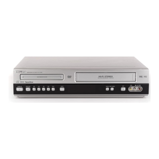
DVD-VCR Player
SECTION 1 SUMMARY
PRODUCT SAFETY SERVICING
GUIDELINES FOR VIDEO PRODUCTS
SERVICING PRECAUTIONS
SERVICE INFORMATION FOR EEPROM IC SETTING
SPECIFICATIONS
DIRECTIONS FOR USE
SECTION 2 CABINET & MAIN CHASSIS
1. EXPLODED VIEWS
1. CABINET AND MAIN FRAME SECTION
2. PACKING ACCESSORY SECTION
SECTION 3 ELECTRICAL
OVERALL BLOCK DIAGRAM
VCR PART
ELECTRICAL ADJUSTMENT PROCEDURES
ELECTRICAL TROUBLESHOOTING GUIDE
1. POWER(SMPS) CIRCUIT
2. SYSTEM/KEY CIRCUIT
3. SERVO CIRCUIT
4. Y/C CIRCUIT
5. HI-FI CIRCUIT
6. TUNER/IF CIRCUIT
BLOCK DIAGRAMS
1. POWER(SMPS) BLOCK DIAGRAM
2. TU/IF, NICAM & A2 BLOCK DIAGRAM
3. VPS BLOCK DIAGRAM
4. Y/C BLOCK DIAGRAM
5. HI-FI BLOCK DIAGRAM
6. SYSTEM BLOCK DIAGRAM
CIRCUIT DIAGRAMS
1. POWER(SMPS) CIRCUIT DIAGRAM
2. TU/IF, NICAM & A2 CIRCUIT DIAGRAM
3. A/V CIRCUIT DIAGRAM
4. HI-FI CIRCUIT DIAGRAM
5. SCART(JACK) CIRCUIT DIAGRAM
6. SYSTEM CIRCUIT DIAGRAM
7. TIMER CIRCUIT DIAGRAM
• WAVEFORM & VOLTAGE SHEET
• CIRCUIT VOLTAGE CHART
PRINTED CIRCUIT DIAGRAMS
1. MAIN P.C.BOARD
©
Copyright 2003 Philips Consumer Electronics B.V. Eindhoven, The Netherlands.
All rights reserved. No part of this publication may be reproduced, stored in a
retrieval system or transmitted, in any form or by any means, electronic,
mechanical, photocopying, or otherwise without the prior permission of Philips.
Published by MW 0365 Service PaCE
1-1
2. SMPS P.C.BOARD
3. KEY P.C.BOARD
1-3
4. TIMER P.C.BOARD
1-4
DVD PART
1-5
ELECTRICAL TROUBLESHOOTING
1-6
GUIDE & WAVEFORMS
1-7
1. SYSTEM OPERATION FLOW
2. TEST & DEBUG FLOW
2-1
DETAILS AND WAVEFORMS ON
2-2
SYSTEM TEST AND DEBUGGING
2-2
1. SYSTEM 27MHZ CLOCK,
2-3
RESET, FLASH R/W SIGNAL
3-1
2. SDRAM CLOCK
3. TRAY OPEN/CLOSE SIGNAL
3-2
4. SLED CONTROL RELATED SIGNAL (NO DISC CONDITION)
5. LENS CONTROL RELATED SIGNAL (NO DISC CONDITION)
3-3
6. LASER POWER CONTROL RELATED SIGNAL
3-4
3-4
7. DISC TYPE JUDGEMENT WAVEFORM
3-7
8. FOCUS ON WAVEFORM
3-8
9. SPINDLE CONTROL WAVEFORM (NO DISC CONDITION)
3-11
10. TRACKING CONTROL RELATED SIGNAL
3-15
3-18
11. RF WAVEFORM
3-20
12. MT1379 AUDIO OPTICAL AND COAXIAL
3-20
OUTPUT (ASPDIF)
3-22
13. MT1379 VIDEO OUTPUT WAVEFORM
3-23
14. AUDIO OUTPUT FROM AUDIO DAC
3-24
BLOCK DIAGRAMS
3-26
1. OVERALL BLOCK DIAGRAM
3-28
2. SERVO BLOCK DIAGRAM
3-30
3. MPEG & MEMORY BLOCK DIAGRAM
3-30
4. VIDEO & AUDIO BLOCK DIAGRAM
3-32
CIRCUIT DIAGRAMS
3-34
1. SYSTEM CIRCUIT DIAGRAM
3-36
2. RF & DSP SERVO CIRCUIT DIAGRAM
3-38
3. AUDIO CIRCUIT DIAGRAM
3-40
4. AV/JACK CIRCUIT DIAGRAM
3-42
• CIRCUIT VOLTAGE CHART
3-44
PRINTED CIRCUIT DIAGRAMS
3-46
1. MAIN P.C.BOARD
3-50
3-50
SECTION 4 MECHANISM
Printed in the Netherlands
(NO DISC CONDITION)
(SYSTEM CHECKING)
Subject to modification
DVD755VR
DVD755VR /00
DVD755VR /02
DVD755VR /05
DVD755VR /14
3-52
3-52
3-52
3-54
3-54
3-55
3-61
3-61
3-61
3-62
3-65
3-65
3-66
3-66
3-68
3-69
3-70
3-71
3-71
3-72
3-73
3-75
3-75
3-76
3-77
3-78
3-79
3-79
3-81
3-83
3-85
3-87
3-91
3-91
4-1
EN 3122 785 13520
Advertisement
Chapters
Table of Contents
Troubleshooting

Related Manuals for Philips DVD755VR


Summary of Contents for Philips DVD755VR
- Page 1 All rights reserved. No part of this publication may be reproduced, stored in a retrieval system or transmitted, in any form or by any means, electronic, mechanical, photocopying, or otherwise without the prior permission of Philips. Published by MW 0365 Service PaCE...
-
Page 2: Section 1 Summary
CONTENTS SECTION 1 ..SUMMARY SECTION 2 ..CABINET & MAIN CHASSIS SECTION 3 ..ELECTRICAL SECTION 4 ..MECHANISM OF VCR PART SECTION 5 ..MECHANISM OF DVD PART SECTION 6 . - Page 3 SECTION 1 SUMMARY CONTENTS PRODUCT SAFETY SERVICING GUIDELINES FOR VIDEO PRODUCTS ..1-3 SERVICING PRECAUTIONS .................. 1-4 SERVICE INFORMATION FOR EEPROM IC SETTING ........1-5 SPECIFICATIONS ....................1-6...
-
Page 4: Product Safety Servicing Guidelines For Video Products
PRODUCT SAFETY SERVICING GUIDELINES FOR VIDEO PRODUCTS CAUTION : DO NOT ATTEMPT TO MODIFY THIS PRODUCT IN ANY WAY, SUBJECT : X-RADIATION NEVER PERFORM CUSTOMIZED INSTALLATIONS WITHOUT MANUFAC- 1. BE SURE PROCEDURES AND INSTRUCTIONS TO ALL SERVICE PER- TURER’S APPROVAL. UNAUTHORIZED MODIFICATIONS WILL NOT ONLY SONNEL COVER THE SUBJECT OF X-RADIATION. -
Page 5: Servicing Precautions
SERVICING PRECAUTIONS CAUTION : Before servicing the VCR+DVD covered by this Electrostatically Sensitive (ES) Devices service data and its supplements and addends, read and fol- Some semiconductor (solid state) devices can be damaged low the SAFETY PRECAUTIONS. NOTE : if unforeseen cir- easily by static electricity. -
Page 6: Service Information For Eeprom Ic Setting
MASKROM : R00 cursor Up/Down key. EEPROM : R00 LG CODE • For PHILIPS model, change a remocon key by using following JIG key. PHILIPS MODEL : FRONT FF + FRONT REC MODEL NAME... -
Page 7: Specifications
SPECIFICATIONS DVD PART Power supply AC 220~230V, 50Hz Power consumtion Mass 5.4kg External dimensions 430 x 97.5 x 360 (W x H x D) Signal system PAL 625/50, NTSC 525/60 Laser Semiconductor laser, wavelength 650nm Frequency range (digital audio) 4 Hz to 20 kHz Signal-to-noise ratio (digital audio) More than 100 dB (EIAJ) Audio dynamic range (digital audio) -
Page 8: Directions For Use
Directions for Use... -
Page 27: Section 2 Cabinet & Main Chassis
SECTION 2 CABINET & MAIN CHASSIS CONTENTS 1. EXPLODED VIEWS ........................2-2 1. Cabinet and Main Frame Section ...................2-2 2. Packing Accessory Section ....................2-3... -
Page 28: Exploded Views
EXPLODED VIEWS 1. Cabinet and Main Frame Section OPTIONAL PARTS... -
Page 29: Packing Accessory Section
2. Packing Accessory Section 810 CABLE ASS'Y, RF CABLE, COAXIAL PLUG ASS'Y(YELLOW) PLUG ASS'Y(RED/WHITE) 813 PLUG ASS'Y(BLACK) BATTERY 821 SCART CABLE REMOCON INSTRUCTION ASSEMBLY PACKING PACKING BOX CARTON OPTIONAL PARTS... -
Page 30: Table Of Contents
SECTION 3 ELECTRICAL CONTENTS OVERALL BLOCK DIAGRAM DVD PART ......3-2 VCR PART ELECTRICAL TROUBLESHOOTING GUIDE & WAVEFORMS ........3-54 ELECTRICAL ADJUSTMENT 1. SYSTEM OPERATION FLOW ......3-54 PROCEDURES ............3-3 2. TEST & DEBUG FLOW ........3-55 ELECTRICAL TROUBLESHOOTING DETAILS AND WAVEFORMS ON GUIDE ................3-4 SYSTEM TEST AND DEBUGGING ....3-61... -
Page 31: Overall Wiring Diagram
OVERALL WIRING DIAGRAM A_MUTE_R A_MUTE_L 6DAC_MUTE D_A_R_OUT D_A_L_OUT C_V_OUT(DVD) Pr/R Pb/B PDV03 PMD02 DATA DATA RESET K.RTN OPTICAL COAXIAL S/COMPO PVD02 PMD01 TIMER 12VA(DRUM) 5.0V 5.3VA PMP01 ERASE FULL P3D03 A.PB A.REC A/E(-) A/E(+) CTL(-) CTL(+) P3D02 DRUM DFG/FG 12VA(DRUM) MOTOR I-limit REV'H'... -
Page 32: Vcr Part
VCR PART ELECTRICAL ADJUSTMENT PROCEDURES 1. Servo Adjustment 1) PG Adjustment • Test Equipment a) OSCILLOSCOPE C) PAL MODEL : PAL SP TEST TAPE b) NTSC MODEL : NTSC SP TEST TAPE • Adjustment And Specification MODE MEASUREMENT POINT ADJUSTMENT POINT SPECIFICATION V.Out PLAY... -
Page 33: Electrical Troubleshooting Guide
ELECTRICAL TROUBLESHOOTING GUIDE 1. Power(SMPS) CIRCUIT (1) No 5.3VA (SYS/Hi-Fi/TUNER) (2) No 12VA (TO CAP, DRUM MOTOR) NO 5.3VA. NO 12VA. Replace the F101. Is the Vcc(13V) supplied to Check or Replace Is the F101 normal? (Use the same Fuse) (+) terminal in D115, D117? the D110. - Page 34 (4) No 5V (TO DVD) (5) No 33V (TUNER) NO 5V. No 33V. Is 5.3VA put into Check the 5.3VA Line Check. Is Timer H “L”? the Q160 Emitter? Timer’H’ Signal. Is the Q162 Base Check the Power Check or Replace “H”? Control.
- Page 35 (8) No 3.3V(TO DVD) (9) No 27V(TO CAP) NO 3.3V. NO 27V. Check or Replace Check the HSR ‘H’ Is Vcc(4V) supplied Is HSR ‘H’ ‘H’? to IC152 Pin1? the D111. Signal from µ-com. Check the Power Is the Q162 Base Is 0V put into the Replace Q154.
-
Page 36: System/Key Circuit
2. SYSTEM/KEY CIRCUIT (1) AUTO STOP Auto Stop Does the SW25 waveform Check the Drum Motor appear at the IC501 signal. Pin105? Do T/UP Reel Pulses Do the T-UP Reel Pulses Does 5.2V appear at the appear at the Q514 appear at the IC501 Pin49? RS501? Base terminal ? -
Page 37: Servo Circuit
3. SERVO CIRCUIT (1) Unstable Video in PB MODE Unstable Video in PB Mode. Does the Noise level of the screen change periodically? Do the CTL pulses appear Is adjusting the height of at the IC501 Pin8? the CTL Head accurate? Does the CFG waveform Readjust the height of the appear at the IC501... - Page 38 2. SERVO CIRCUIT (3) When the Capstan Motor doesn’t run, When the Capstan Motor doesn’t run, Refer to “SMPS(CAPSTAN/12Volt) Does 12VA appear at the PMC01? Trouble Shooting”. Does 2.8V appear at the PMC01? Check the PMC01 and the Capstan Does the PWM signal appear at the IC501 Pin108? Motor Ass’y.
- Page 39 (4) KEY doesn’t working KEY doesn’t working. Is 5V applied to the IC501 Refer to “SMPS 5.3VA Pin36? Trouble Shooting”. Does LED or FLD change Replace the defective when a function button is switches. pressed? 3-10...
-
Page 40: Y/C Circuit
4. Y/C CIRCUIT (1) No Video in EE Mode, No Video in EE Mode Does the Video signal Check the 24Pin of Tuner. appear at the IC301 Pin48? Is 5V applied to the IC301 Check the 5.2VT, 5.3VA Pins18, 24, 42, 55, 72, 91? Line. - Page 41 3. Y/C CIRCUIT (2) When the Y(Luminance) signal doesn’t appear on the screen in PB Mode, Is 5.2VT, 5.3VA applied to the Check the line of the 5.2VT, 5.3VA Line. (Power Circuit) IC301 Pins24, 42, 55, 72, 91? Is the I C Bus siganl applied Refer to ‘SYSTEM I C BUS...
- Page 42 3. Y/C CIRCUIT (3) When the C(Color) signal doesn’t appear on the screen in PB Mode, Is 5.2VT/5.3VA applied to the Check the line of the 5.2VT/ 5.3VA Line. (Power Circuit) IC301 Pins24, 42, 55, 72, 91. Is the Color Rotary signal Check the Color Rotary applied to the IC301 Circuit.
- Page 43 3. Y/C CIRCUIT (4) When the Video signal doesn’t appear on the screen in REC Mode, Is the EE signal normal? Check EE Mode. Is 5.2VT/5.3VA applied to the Check the line of the 5.2VT/ IC301 Pins24,42,55,72,91? 5.3VA Line.(Power Circuit) Does PB Mdoe operate Check PB Mode.
-
Page 44: Hi-Fi Circuit
5. Hi-Fi CIRCUIT (A) No Sound(EE Mode) No Sound. Check the TU Audio of IC801 Check the IC751 Pins30, 31. Pins2, 3. Check the DVD Audio of IC801 Check the DVD MODULE. (PMD02 Pins13, 15). Pins4, 5. Check the AV1 Audio of IC801 Check the Scart1 Jack. - Page 45 3. Y/C CIRCUIT (B) Hi-Fi Playback PB mode No Sound. Check the Vcc of IC801 Check Power 5.2V, 12VT. (Pins34, 40) Check the Hi-Fi Selection switch. Check IC501 Pin106 (A.H/SW) (IC801 Pin41) and the Tape quality. Is the RF Envelope at IC801 Pin44 over 2Vp-p? Check IC801 Pin42(Data), Check the parts of µ-COM...
- Page 46 Hi-Fi REC. It can’t be recorded Hi-Fi Audio signal. Check Vcc of IC801.(Pins34, 40) Check Power 5V, 12VT. Check ports of µ-COM. Check IC801 Pin42(Data), Pin43(CLOCK). (IC501 pins 59, 60) Check Audio input signal of IC801 Do Audio signals appear at IC801 Pins2, 3(TU.A.), 4, 5(DVD.A.), Pins16, 17? 6, 7(AVI.A.), 8, 9(AV2.A.), 10, 11(AV3.A.).
-
Page 47: Tuner/If Circuit
6. Tuner/IF CIRCUIT (A) No Picture on the TV screen No picture on the TV screen Does the Video signal at Is +33VT applied to TU701 Check 33VT line. the TU701 Pin24. Pin16? Is +5VT applied to TU701 Check 5VT line. Pin13? Does the Clock signal Check the lIC Clock Signal... - Page 48 (B) No Sound No Sound. Check the Vcc of IC751 Pins1, 11, 19, Check 5.2V Line. 22, 33. Check the Tuner SiF signal at IC751 Check the Tuner SIF of TU701 Pin22. Pin2. Check the oscillator of IC751 Pins5, 6. Replace X751 Check the IIC Clock and Data at IC751 Check the Audio of IC751 Pins30, 31.
-
Page 50: Block Diagrams
(R157, Q150, R158, R159, D121, C155) IC103 (BK) (WH) HOT CIRCUIT PWR CTL FROM µ-COM BLOCK PWR CTL 'H' (Q162,R163,R164, R171,C161) FROM µ-COM TIMER 'H' NOTES : Symbol denotes AC ground. COMBI SCART Symbol denotes DC chassis ground. PHILIPS 3-20 3-21... -
Page 51: Tu/If, Nicam & A2 Block Diagram
2. Tu/IF, NICAM & A2 BLOCK DIAGRAM 3. VPS BLOCK DIAGRAM VC02 PD2/ 5.4VA VC01 S.V.W Iref 5.2VT Power) (From CVBS V.out VSUP COMBI SCART VC6's 3-22 3-23... -
Page 52: Y/C Block Diagram
4. Y/C BLOCK DIAGRAM (PB MODE) (REC MODE) V.OUT V.IN3 FRONT V.OUT V.IN4 (MICOM) V.OUT MICOM V.OUT SYNC C.SYNC CLOCK CLOCK DATA DATA C.ROTARY C.ROTARY V.H.SW V.H.SW REC'H' COMBI SCART VC6's 3-24 3-25... -
Page 53: Hi-Fi Block Diagram
5. Hi-Fi BLOCK DIAGRAM VIDEO INPUT BLOCK Hi-Fi/ AUDIO INPUT 36 35 BLOCK Tu A.IN 'L' Tu A.IN 'R' A.OUT 'L' DVD A.IN 'L' A.OUT DVD A.IN 'R' IC802 To JACK A.OUT 'R' IC801 EU1 A.IN 'L' EU1 A.IN 'R' EU2 A.IN 'L' EU2 A.IN 'R' AV2 A.IN 'L'... -
Page 54: System Block Diagram
6. SYSTEM BLOCK DIAGRAM LD(+) LD(-) OTPB LED 'H' IC501 CANAL DET 'H' HD6432197A L/M CONTROL R525, R526 R/C IN(2W) CST SW 2fsc R524, R514, R518, R516, R589, C577, C576, L501, Q504 COMBI SCART VC6's 3-28 3-29... -
Page 55: Circuit Diagrams
2. Voltages are DC-measured with a digital voltmeter MODIFIED OR ALTERED WITHOUT PERMISSION IMPLEMENTATION OF THE LATEST SAFETY AND during Play mode. FROM THE PHILIPS ELECTRONICS CORPORATION. PERFORMANCE IMPROVEMENT CHANGES INTO ALL COMPONENTS SHOULD BE REPLACED ONLY THE SET IS NOT DELAYED UNTIL THE NEW SERVICE WITH TYPES IDENTICAL TO THOSE IN THE ORIGI- LITERATURE IS PRINTED. -
Page 56: Tu/If, Nicam & A2 Circuit Diagram
2. TU/IF, NICAM & A2 CIRCUIT DIAGRAM (COMBI SCART) EE MODE(VIDEO) TU MODE (AUDIO) 3-32 3-33... -
Page 57: A/V Circuit Diagram
3. A/V CIRCUIT DIAGRAM IC301 Pin 69, 68 are defective. PB and Recording is failed. (IC301 doesn’t operate.) Q305 is defective. IC301 Pin70 is defective. EE, PB Screen doesn’t appear. PB COLOR Signal disappear. D301or IC301 Pin 80 REC is defective. IC301 Pin 84 is defective. -
Page 58: Hi-Fi Circuit Diagram
4. Hi-Fi CIRCUIT DIAGRAM IC801 Pins42, 43 aredefective. All Audio is not appear. 44 Pin is defective. Hi-Fi Audio is not appear. OPTIONAL PART (COMBI SCART) 3-36 3-37... -
Page 59: Scart(Jack) Circuit Diagram
5. SCART(JACK) CIRCUIT DIAGRAM OPTIONAL PART (COMBI SCART) 3-38 3-39... -
Page 60: System Circuit Diagram
6. SYSTEM CIRCUIT DIAGRAM SW is defective. Key service dead. Reset is defective. Set dead. IC504 is defective. CLOCK SETTING will not operate. X501 is defective. µ-COM will not operate. X502 is defective. RC501 is defective. R/C will not operate. VCR will not operate. -
Page 61: Timer Circuit Diagram
7. TIMER CIRCUIT DIAGRAM 3-42 3-43... -
Page 62: Waveform & Voltage Sheet
WAVEFORM & VOLTAGE SHEET _ IC301 Oscilloscope Waveform * IC501 Waveform Photographs IC301 Pin IC301 Pins 38,32,31 IC301 Pin IC301 Pin V.HSW DV.SYNC CTL(+) CTL(-) PB mode PB/REC mode REC mode (IC501 Pin 105) (IC501 PIN 109) (IC501 Pin 3) (IC501 Pin4) 1V/10mS 1V/100uS... -
Page 63: Circuit Voltage Chart
• CIRCUIT VOLTAGE CHART MODE MODE MODE MODE MODE MODE MODE PIN NO. PIN NO. PIN NO. PIN NO. PIN NO. PIN NO. PIN NO. I C 2 0 1 4.85 V 4.85 V 4.75 V 1.73 V 1.67 V 2.51 V 1.86 V 0.004 V... - Page 64 MODE PIN NO. 5.6 V 5.58 V 5.59 V Q301 COLECTOR 0.02 V 0.01~4.8V 0.011 V 5.6 V 5.58 V 5.59 V BASE 0.01 V 0.013 V 0.79 V Q7S1 EMITER 0.003 V 0.004 V 0.005 V BASE 0.007 V 0.007 V 0.008 V 5.54 V...
-
Page 65: Printed Circuit Diagrams
PRINTED CIRCUIT DIAGRAMS 1. MAIN P.C.BOARD LOCATION GUIDE 3-50 3-51... -
Page 66: Smps P.c.board
2. SMPS P.C.BOARD 4. KEY P.C.BOARD LOCATION GUIDE 3. TIMER P.C.BOARD LOCATION GUIDE 3-52 3-53... -
Page 68: Dvd Part
DVD PART ELECTRICAL TROUBLESHOOTING GUIDE 1. System operation flow Power On 1. 8032 initializes SERVO, DSP & RISC registers 2. Write RISC code to SDRAM 3. Reset RISC Show LOGO Tray Closed? Tray Close to Closed position SLED at Inner Side? SLED Moves to Inner Position 1. -
Page 69: Test & Debug Flow
2. Test & debug flow TEST Check the AC Vol tage Check the POWER PART Power PCBA (110V or 220V) Switch on the Power PCBA the DC Vol tage outputs OK? Check the POWER PART (5V, 3.3V, 8V, 12V) Make sure the main PCBA don't Is 3.3V and 2.5V DC Check the regulators or diode(D601). - Page 70 RESET or Power On. Flash Check connecti on lines between FLASH Memory operates Show LOGO? & MT1379 and the FLASH access time properly? whether is sui table or not. Check connection lines between SDRAM SDRAM(IC502,IC503) & MT1379 and the works properl y? SDRAM is damaged.
- Page 71 Does the SLED move Check the connection line of Motor Driver STBY to inner side when it is at STBY signal . Pin is High? outter positi on? Check the rel ated circuit of Motor Driver STBY FMSO. Pin is High? Check the amp circuit on SL+ and SL- output motor driver.
- Page 72 Check the laser power circuit Laser turns on when LD01 or LD02 output on MT1336 and connecting to reading disc? properly? power transistor. (Q204, Q205) Collector Check therel ated ci rcuit on voltage of power laser power transi stor transistor is OK? ( Q204, Q205) Check cable connection between transistor couput and pick-up head.
- Page 73 Proper Check connections between signals on A, B, C, Focus ON OK? MT1336 and pick-up head. D of MT1336 Check the related circuit Proper FEO signal on MT1336 FEO sugnal . on MT1336? Check FEO connection between MT1336 and MT1379 Check the related Proper FEO signal Track On OK?
- Page 74 Audio Normal DAC received Check connection between MT1379 Audio output & Audio DAC. (Check VRST#, ACLK, correct data stream? when disc playback? ABCK, ASDAT3) Normal Check the related circuit of Audio DAC Audio DAC. (Check Audio out? (IC401) out Pin 14, 15,18,19) Check Audio filter, amplify, mute circuit.
-
Page 75: Details And Waveforms On System Test And Debugging
DETAILS AND WAVEFORMS ON SYSTEM TEST AND DEBUGGING 1. SYSTEM 27MHz CLOCK,RESET,FLASH R/W SIGNAL 1) MT1379 main clock is at 27MHz(X501) 3.8V, 27MHz FIG 1-1 2) MT1379 & MT1336 reset is high active. Power Cord in 5.2VA PWR_CTL(CN505 PIN 7) M_RESET(CN505 PIN 9) URST(IC501 PIN 188) FIG 1-2... - Page 76 3) RS232 waveform during procedure(Downloading) TXD(J6 PIN3) RXD(J6 PIN 2) FIG 1-3 4) Flash R/W enable signal during download(Downloading) FRD(IC5A1 PIN 28) FWR(IC5A1 PIN 11) FIG 1-4 3-62...
-
Page 77: Sdram Clock
2. SDRAM CLOCK 1) MT1379 main clock is at 27MHz(X501) DCLK = 93MHz, Vp-p=2.2, Vmax=2.7V (IC502,IC503 PIN 35) FIG 2-1 3. TRAY OPEN/CLOSE SIGNAL 1) Tray open/close waveform OPEN((CN203 PIN 3) CLOSE(CN203 PIN 2) TROPEN(IC202 PIN 1) TRCLOSE(IC202 PIN 2) FIG 3-1 3-63... - Page 78 2) Tray close waveform OPEN((CN203 PIN 3) CLOSE(CN203 PIN 2) TROPEN(IC202 PIN 1) TRCLOSE(IC202 PIN 2) FIG 3-2 3) Tray open waveform OPEN((CN203 PIN 3) CLOSE(CN203 PIN 2) TROPEN(IC202 PIN 1) TRCLOSE(IC202 PIN 2) FIG 3-3 3-64...
-
Page 79: Sled Control Related Signal (No Disc Condition)
4. SLED CONTROL RELATED SIGNAL (NO DISC CONDITION) FMSO(2.0V/1.4V/1.0V) (IC501 PIN 19) STBY(5V) – (IC201 PIN 50) SL+(4.7V/3.6V/1.9V) (IC202 PIN 12) SL-(5.3V/3.7V/2.5V) (IC202 PIN 13) FIG 4-1 5. LENS CONTROL RELATED SIGNAL(NO DISC CONDITION) FOSO(1.5V/1.4V/1.3V) (IC501 PIN 12) F+(4.0V/3.6V/3.2V) (IC202 PIN 9) F-(4.0V/3.6V/3.2V) (IC202 PIN 8) FIG 5-1... -
Page 80: Laser Power Control Related Signal(No Disc Condition)
6. LASER POWER CONTROL RELATED SIGNAL(NO DISC CONDITION) MDI1(0V/180mV) (IC201 PIN 124) LD01(5.0V//3.5V) IC201 PIN 125) LD02(5.0V/3.6V) (IC201 PIN 126) FIG 6-1 7. DISC TYPE JUDGEMENT WAVEFORM F+(IC202 PIN 9) FE(IC201 PIN 18) RFL(IC201 PIN 19) FIG 7-1 (DVD) 3-66... - Page 81 F+(IC202 PIN 9) FE(IC201 PIN 18) RFL(IC201 PIN 19) FIG 7-2 (DVD) F+(IC202 PIN 9) FE(IC201 PIN 18) RFL(IC201 PIN 19) FIG 7-3 (CD) 3-67...
-
Page 82: Focus On Waveform
F+(IC202 PIN 9) FE(IC201 PIN 18) RFL(IC201 PIN 19) FIG 7-4 (CD) 8. FOCUS ON WAVEFORM FE(IC201 PIN 18) FOSO(IC501 PIN12) F+(IC202 PIN 9) F-(IC202 PIN 8) FIG 8-1 (DVD) 3-68... -
Page 83: Spindle Control Waveform (No Disc Condition)
FE(IC201 PIN 18) FOSO(IC501 PIN12) F+(IC202 PIN 9) F-(IC202 PIN 8) FIG 8-2 (CD) 9. SPINDLE CONTROL WAVEFORM (NO DISC CONDITION) DMSO(1.4V/1.8V) (IC501 PIN 18) SP-(3.6V/2.4V) (IC202 PIN 10) SP+(3.6V/4.8V) (IC202 PIN 11) FIG 9-1 3-69... -
Page 84: Tracking Control Related Signal(System Checking)
10. TRACKING CONTROL RELATED SIGNAL(System checking) TE(IC201 PIN 21) TRSO(IC501 PIN 13) T-(IC202 PIN 7) T+(IC202 PIN 6) FIG 10-1(DVD) TE(IC201 PIN 21) TRSO(IC501 PIN 13) T-(IC202 PIN 7) T+(IC202 PIN 6) FIG 10-2(CD) 3-70... -
Page 85: Rf Waveform
11. RF WAVEFORM RFOP(2.3V/1.1V) (IC201 PIN 6) RFON(0.8V/2.0V) (IC201 PIN 7) FIG 11-1 12. MT1379 AUDIO OPTICAL AND COAXIAL OUTPUT (ASPDIF) (IC501 PIN 153) FIG 12-1 3-71... -
Page 86: Mt1379 Video Output Waveform
13. MT1379 VIDEO OUTPUT WAVEFORM 1) Full colorbar signal(CVBS) (IC604 PIN 23) FIG 13-1 2) Y (IC604 PIN 21) FIG 13-2 3-72... -
Page 87: Audio Output From Audio Dac
3) C (IC604 PIN 26) FIG 13-3 14. AUDIO OUTPUT FROM AUDIO DAC 1) Audio L/R (JK601 PIN 4,5) FIG 14-1 3-73... - Page 88 2) Audio related Signal ASDATA3 ASDAT3(IC501 PIN 157) ABCK(IC501 PIN 148) ALRCK(IC501 PIN 149) FIG 14-2 3-74...
-
Page 89: Block Diagrams
BLOCK DIAGRAMS 1. Overall Block Diagram MA11,BA1 DQM[2:3] MUTE DQ[16:31] ASPDIF Y[1:6] CVBS ASPECT DQM[0:1] DQ[00:15] URST F+,F-,T+,T- SP+,SP- SL+,SL- LOAD+,LOAD- DECK MECHANISM COMBI SCART MTK MODEL 3-75... -
Page 90: Servo Block Diagram
2. SERVO Block Diagram DQ[16:31] DQ[0:15] COMBI SCART MTK MODEL 3-76... -
Page 91: Mpeg & Memory Block Diagram
3. MPEG & MEMORY Block Diagram AD[0:7] A[0:19] DQ[16:31] PWR,PCE,PRD DQM2,DQM3 CS,DCKE,MA[0:10] DCLK,WE,CAS,RAS M_REQ VFD_TXD VFD_SCK DQ[0:15] DQM0,DQM1 VFD_RXD URST,S_REQ COMBI SCART MTK MODEL 3-77... -
Page 92: Video & Audio Block Diagram
4. VIDEO & AUDIO Block Diagram COMBI SCART MTK MODEL 3-78... -
Page 94: Circuit Diagrams
CIRCUIT DIAGRAMS 1. SYSTEM CIRCUIT DIAGRAM No Power on Video signal not appeared System not working or screen is abnormal Program download fail COMBI SCART MTK Digitron all not display Video signal Y '03. 3. 25 SR17444A System not working Video signal Color 3-79 3-80... -
Page 95: Rf & Dsp Servo Circuit Diagram
2. RF & DSP SERVO CIRCUIT DIAGRAM CD/DVD LD will not on COMBI SCART MTK '03. 3. 25 SR17445A 3-81 3-82... -
Page 96: Audio Circuit Diagram
3. AUDIO CIRCUIT DIAGRAM COMBI SCART MTK '03. 3. 25 SR17447A 3-83 3-84... -
Page 97: Av/Jack Circuit Diagram
4. AV/JACK CIRCUIT DIAGRAM COMBI SCART MTK '03. 3. 25 SR17446A 3-85 3-86... -
Page 98: Circuit Voltage Chart
• CIRCUIT VOLTAGE CHART IC201 IC202 IC501 IC502 IC505 IC510 IC5A1 IC401 IC402 IC5C1 IC201 IC202 IC501 IC502 IC505 IC510 IC5A1 IC401 IC402 IC5C1 (MT1336E) (MOTOR) (MT1379) (SDRAM) (EEPROM) (BUFFER) (FLASH) (CS4391) (AMP) (MM1623XFBE) (MT1336E) (MOTOR) (MT1379) (SDRAM) (EEPROM) (BUFFER) (FLASH) (CS4391) (AMP) - Page 99 Q201 Q202 Q203 Q204 IC201 IC202 IC501 IC502 IC505 IC510 IC5A1 IC401 IC402 IC5C1 (MT1336E) (MOTOR) (MT1379) (SDRAM) (EEPROM) (BUFFER) (FLASH) (CS4391) (AMP) (MM1623XFBE) STOP PLAY STOP PLAY STOP PLAY STOP PLAY PIN STOP PLAY STOP PLAY STOP PLAY STOP PLAY STOP PLAY STOP PLAY STOP PLAY STOP PLAY STOP PLAY STOP PLAY 5.14 4.34...
-
Page 100: Printed Circuit Diagrams
PRINTED CIRCUIT DIAGRAMS 1. MAIN P.C.BOARD LOCATION GUIDE 3-91 3-92... -
Page 102: Section 4 Mechanism
SECTION 4 MECHANISM OF VCR PART CONTENTS DECK MECHANISM PARTS DECK MECHANISM ADJUSTMENT LOCATIONS • Tools and Fixtures for Service ....4-12 1. Mechanism Alignment Position Check..4-13 • Top View............4-1 2. Preparation for Adjustment......4-14 • Bottom View ..........4-1 3. Checking Torque ........4-14 4. -
Page 103: Top View
DECK MECHANISM PARTS LOCATIONS • Top View Procedure Fig- Part Fixing Type Starting 1 Drum Assembly 3 Screw 2 Plate Top 2 Hook 3 Holder Assembly CST Chassis Hole 4 Opener Door Chassis Hole 5 Bracket Assembly 3 Hook L/D Motor 2,3,4 6 Gear Assembly Rack F/L 1 Hook, Chassis Hole A-2... - Page 104 DECK MECHANISM DISASSEMBLY Stator (S2) (S2) (S3) Drum Motor (S3) Rotor Drum Sub Assembly (Fig. A-1-1) Drum FPC Carbon Brush (S1) (S1) (S1) Holder FPC Fig. A-1 (Fig. B-1) 1. Drum Assembly (Fig. A-1-1) 1) Unplug the Drum FPC Connector. 2) Remove three Screws(S1) on bottom side and separate the Drum assembly.
- Page 105 DECK MECHANISM DISASSEMBLY (Fig. A-2-1) Plate Top (B') (Fig. A-2-2) Holder Assembly CST (Fig. A-2-6) Arm Assembly F/L (C1) (Fig. A-2-7) Lever Assembly S/W (H8) Bracket Assembly L/D Motor Spring Lever S/W (Fig. A-2-4) (C') (E') Opener Door (Fig. A-2-3) (H6) Chassis Gear Assembly Rack F/L...
-
Page 106: Bracket Assembly L/D Motor
DECK MECHANISM DISASSEMBLY 2. Plate Top (Fig. A-2-1) 2) Unhook three Hooks(H3, H4, H5) on bottom side of the Chassis, lift up the Bracket Assembly L/M and disassem- 1) Pull the (B) portion of the Plate Top back in direction of ble the Bracket Assembly L/D Motor. - Page 107 DECK MECHANISM DISASSEMBLY Arm Assembly Cleaner (Fig. A-3-1) (S4) Base Assembly A/C Head (Fig. A-3-3) Head F/E (Fig. A-3-2) Chassis Fig. A-3 9. Arm Assembly Cleaner (Fig. A-3-1) 11. Base Assembly A/C Head (Fig. A-3-3) 1) Breakaway the (A) portion as Fig. A-3-1 from the 1) Remove the Screw(S4) and lift the Base Assembly A/C embossing of the Chassis, turn the Arm assembly Head up.
- Page 108 DECK MECHANISM DISASSEMBLY Arm Assembly Tension (Fig. A-4-3) (H11) Spring TB Brake Assembly T (Fig. A-4-1) Spring Tension Reel S Reel T (Fig. A-4-4) (Fig. A-4-4) Spring RS Brake Assembly RS (Fig. A-4-2) (H12) (H9) (H10) Base Tension Chassis Fig. A-4 12.
- Page 109 DECK MECHANISM DISASSEMBLY Opener Lid (Fig. A-5-2) Assembly Pinch (Fig. A-5-3) Base Assembly P4 Lever T/up (H13) (Fig. A-5-1) (Fig. A-5-4) (H13) Arm T/up (Fig. A-5-5) Chassis Fig. A-5 16. Base Assembly P4 (Fig. A-5-1) NOTE 1) Breakaway the (A) portion of the Base Assembly P4 from When reassembling, confirm the (C) portion of the Arm the embossing of the Chassis.
- Page 110 DECK MECHANISM DISASSEMBLY Belt Capstan (Fig. A-6-1) Motor Capstan (Fig. A-6-2) Washer(W1) Clutch Assembly D35 (Fig. A-6-4) (L1) (L1) Brake Assembly Capstan (Fig. A-6-5) Lever F/R (Fig. A-6-3) (L2) Chassis (S5) Fig. A-6 20. Belt Capstan (Fig. A-6-1)/ 22. Clutch Assembly D35 (Fig. A-6-4) Motor Capstan (Fig.
- Page 111 DECK MECHANISM DISASSEMBLY (H14) Gear Cam Hole(B) Gear Cam (Fig. A-7-2) Gear Drive Hole(A) Washer (W2) Gear Sector (Fig. A-7-3) Plate Slider Gear Drive (Fig. A-7-4) (Fig. A-7-1) Lever Tension (Fig. A-7-5) Lever spring (L3) (Fig. A-7-6) Gear Drive Hole(C) Base Loading (H15) (H16)
- Page 112 DECK MECHANISM DISASSEMBLY Gear Assembly P2 Hole Gear Assembly P3 Hole Gear Assembly P3 (Fig. A-8-2) Gear Sector Hole(A) Lever Spring Boss Gear Assembly P2 Plate Slider Hole(B) (Fig. A-8-1) Chassis Base Assembly P3 (Fig. A-8-4) Base Assembly P2 (Fig. A-8-3) Fig.
- Page 113 DECK MECHANISM DISASSEMBLY (S7) Base Tension Base Loading (Fig. A-9-2) Arm Assembly Idler (Fig. A-9-1) (Fig. A-9-3) Chassis Fig. A-9 31. Base Loading (Fig. A-9-1) 33. Arm Assembly Idler (Fig. A-9-3) 1) Remove the Screw(S7). 1) Make narrower the two parts, (B) and (C), as Fig. A-9-3. 2) Lift the Base Loading up.
-
Page 114: Deck Mechanism Adjustment
DECK MECHANISM ADJUSTMENT • Tools and Fixfures for Service 1. Cassette Torque Meter 2. Alignment Tape 3. Torque Gauge SRK-VHT-303(Not SVC part) Parts No NTSC: DTN-001 600g.Cm ATG Parts No: D00-D006 PAL:DTN-0002 Parts No:D00-D002 4. Torque Gauge Adaptor 5. Post Height Adjusting Driver 6. -
Page 115: Mechanism Alignment Position Check
DECK MECHANISM ADJUSTMENT 1. Mechanism Alignment Position Check Purpose:To determine if the Mechanism is in the correct position, when a Tape is ejected. Test Conditions (Mechanism Test Equipment/ Fixture Check Point Condition) • Mechanism and Mode Switch Position • Blank tape •... -
Page 116: Checking Torque
DECK MECHANISM ADJUSTMENT 2. Preparation for Adjustment (To set the cassette without tape. Cover the holes of the End Sensors at the both sides of Deck Mechanism of the loading state the Chassis to prevent a light leak. without inserting a cassette tape). Then the Deck Mechanism drives to the Stop Mode. -
Page 117: Guide Roller Height Adjustment
DECK MECHANISM ADJUSTMENT 4.Guide Roller Height Adjustment Purpose: To regulate the height of the tape so that the bottom of the tape runs along the tape guide line on the Lower Drum. 4-1. Preliminary Adjustment Test Equipment/ Fixture Test Conditions (Mechanism Condition) Adjustment Point •... -
Page 118: Audio/Control (A/C) Head Adjustment
DECK MECHANISM ADJUSTMENT 5. Audio/Control (A/C) Head Adjustment Purpose: To insure that the tape passes accurately over the Audio and Control Tracks in exact alignment of the both Record and Playback Modes. 5-1. Preliminary Adjustment (Height and Tilt Adjustment) Perform the Preliminary Adjustment, when there is no Audio Output Signal with the Alignment Tape. Test Equipment/ Fixture Test Conditions (Mechanism Condition) Adjustment Point... -
Page 119: X-Value Adjustment
DECK MECHANISM ADJUSTMENT 5-2. Confirm that the tape passes smoothly (2) If folding or curling is observed at the top of it then slowly turn the Tilt Adjustment Screw(C) in the between the Take-up Guide and Pinch counterclockwise direction. Roller(using a mirror or the naked eye). 1) After completing Step 5-1.(Preliminary Adjustment), check NOTE: that the tape passes around the Take-up Guide and Pinch... - Page 120 DECK MECHANISM ADJUSTMENT 7. Adjustment after Replacing Drum Assembly (Video Heads) Purpose: To correct for shift in the Roller Guide and X value after replacing the Drum. Test Conditions Test Equipment/ Fixture Connection Point Adjustment Points (Mechanism Condition) • CH-1: PB RF Envelope •...
-
Page 121: Check Before Starting Repairs
MAINTENANCE/INSPECTION PROCEDURE 1. Check before starting repairs The following faults can be remedied by cleaning and oil- ing. Check the needed lubrication and the conditions of cleanliness in the unit. Check with the customer to find out how often the unit is used, and then determine that the unit is ready for inspec- tion and maintenance. -
Page 122: Required Maintenance
MAINTENANCE/INSPECTION PROCEDURE 2. Required Maintenance 4. Supplies Required for Inspection and Maintence The recording density of a VCR(VCP) is much higher than that of an audio tape recorder. VCR(VCP) components must (1) Grease : Kanto G-311G (Blue) or equivalent be very precise, at tolerances of 1/1000mm, to ensure com- (2) Isopropyl Alcohol or equivalent patibility with the other VCRs. - Page 123 MAINTENANCE/INSPECTION PROCEDURE 5-2) Greasing (2) Periodic greasing Grease specified locations every 5,000 hours. (1) Greasing guidelines 1) Loading Path Inside & Top side 6) Plate Slider Guide Sections Apply grease, with a cleaning patch. Do not use exces- 2) Base Assembly P2,P3 stopper 7) Plate Slider Guide Sections sive grease.
- Page 124 MAINTENANCE/INSPECTION PROCEDURE Lever, F/R, Base, Tension GEAR AY, P2 & P3 Boss Lever, F/R Base, Tension Clutch (G-754. Yellow) Arm Tension Guide Hole 4-22...
-
Page 125: Deck Mechanism
MECHANISM TROUBLESHOOTING GUIDE 1.Deck Mechanism Auto REW doesn't work. Is the output of END sensor of supply side "H"? “H”: more than 3.5V “L”: less than 0.7V~1V Is the Vcc. voltage of End Check the syscon power. sensor 5V? Replace the End sensor. Is the voltage across IR LED Replace the IR LED. - Page 126 MECHANISM TROUBLESHOOTING GUIDE AUTO STOP. (PLAY/CUE/REV) Check alignment positions (page 4-13). In Play/Cue/Rev, Is the Pinch Roller in contact with the Is the output of DFG, DPG OK? Replace the Drum Motor. Capstan Shaft? Are there T/up and Supply Reel Check the Servo, Syscon.
- Page 127 MECHANISM TROUBLESHOOTING GUIDE In PB mode Tape Presence not sensed. Is the Pinch Roller attached Check Alignment positions to the Capstan Motor Shaft? (page 4-13). Does the T/Up Reel turn? Is the Belt ok? Replace the Belt. Check the Clutch and Idler Does the Capstan Motor turn? Assembly.
-
Page 128: Front Loading Mechanism
MECHANISM TROUBLESHOOTING GUIDE 2. Front Loading Mechanism Cassette cannot be inserted. Does the Lever Assembly Is the Lever Assembly Switch Replace or add the Lever Switch work? Spring damaged or omitted? Assembly Switch Spring. Does the CST IN Switch work Replace the CST IN Switch. - Page 129 MECHANISM TROUBLESHOOTING GUIDE Cassette does not load. Does the cassette insert? Does the Opener Lid work? Does the Gear Assembly Rack F/L Replace the Opener Lid. work? Replace the Gear Rack F/L. Does the Opener Door work? Check the opener Door assembled Does the Arm Assembly F/L work? correctly.
- Page 130 EXPLODED VIEWS 1. Front Loading Mechanism Section 4-28...
- Page 131 EXPLODED VIEWS 2. Moving Mechanism Section(1) OPTIONAL PART 4-29...
- Page 132 EXPLODED VIEWS 3. Moving Mechanism Section(2) OPTIONAL PART 4-30...
- Page 133 MEMO...
- Page 134 SECTION 5 MECHANISM OF DVD PART CONTENTS EXPLODED VIEW 1. Deck Mechanism Exploded View .................5-1...
- Page 135 EXPLODED VIEWS 1. DECK Mechanism Exploded View 024A 024B 024A 011A 015A 015B 015C...
- Page 136 C273 9965 000 18560 0.033µF 50V K (X) 1508 R/ C541 4822 124 11947 10µF 20% 16V FRONT PWB DVD755VR /02 C542 9965 000 18556 0.1µF 50V Z (F) 1508 R/TP C274 9965 000 18561 470pF 50V J 1508 R/TP C543 4822 124 11947 10µF 20% 16V...
- Page 137 3141 018 51690 TRA SM 2SK3018 R427 4822 051 30102 1k 5% 0,062W Q204 4822 130 61269 2SA1037KQ MAIN PWB DVD755VR /02 R501 4822 117 12902 8k2 1% 0.063W 0603 Q205 4822 130 61269 2SA1037KQ 9965 000 18576 750k Ω 1/16 W 5% 1608 R/...
- Page 138 C306 9965 000 18592 1200P 50V K B 2.0X1.25 R/ C502 4822 124 23056 47µF 20% 16V C5S3 9965 000 18597 0.022µF 50V K B 2.0X1.2 R/ C503 4822 124 12052 220µF 20% 6,3V C307 4822 124 23053 1µF 20% 63V C504 4822 124 12052 220µF 20% 6,3V C706...
- Page 139 C864 4822 124 23053 1µF 20% 63V Q303 4822 130 10491 KTC3875S-GR-T1(ALG) R501 4822 117 11373 100Ω 1% RC12H 0805 C869 4822 124 11947 10µF 20% 16V Q304 4822 130 10491 KTC3875S-GR-T1(ALG) R502 4822 117 11373 100Ω 1% RC12H 0805 C870 9965 000 18587 0.1µF 2012 50V 80%,-20% Q305...
- Page 140 1,25W L123 9965 000 19212 CHOCK(22mH ) 5MM TOKO R842 4822 117 13577 330Ω 1% RC12H 0805 1,25W PSU PWB DVD755VR /xx L125 9965 000 19213 CHOCK ,20µH R850 4822 117 11373 100Ω 1% RC12H 0805 KWANGSUNG LEAD CU R851 4822 117 11373 100Ω...
- Page 141 SW60 ASSEMBLY 9965 000 19257 THVV502GAA POSTECH Various DC 12 V 5- SW60 FRONT PWB DVD755VR /00 9965 000 19245 VCR PHILIPS COMBI 9965 000 19257 THVV502GAA POSTECH DC 12 V 5- Various VCR MECHANICAL DVD755VR /xx C601 4822 124 11947 10µF 20% 16V 9965 000 18512 DOOR.CASE...
- Page 142 C293 4822 124 23056 47µF 20% 16V C576 9965 000 18556 0.1µF 50V Z (F) 1508 R/TP L613 9965 000 18575 HB-1M2012-102JT C295 4822 124 11947 10µF 20% 16V C577 9965 000 18556 0.1µF 50V Z (F) 1508 R/TP CERATECH TP C296 9965 000 18556 0.1µF 50V Z (F) 1508 R/TP C578...
- Page 143 4822 051 30102 1k 5% 0,062W R427 4822 051 30102 1k 5% 0,062W C362 4822 124 23056 47µF 20% 16V MAIN PWB DVD755VR /00 R501 4822 117 12902 8k2 1% 0.063W 0603 C363 9965 000 18586 0.01µF 50V 5% B(5YP) 2012 9965 000 18576 750k Ω...
- Page 144 C575 9965 000 18602 1000P 50V K B 2.0X1.25 R/ C814 4822 124 23056 47µF 20% 16V L305 9965 000 18641 100M K 6X6 L5 TP C815 4822 124 11947 10µF 20% 16V L307 9965 000 18640 10µH 5% TP 3X5 TR5 C576 9965 000 18611 27P 50V J COG 2.0X1.2 R/ C816...
- Page 145 R901 4822 117 11383 12k 1% 0,1W R557 4822 051 20273 27k 5% 0,1W R902 4822 117 10833 10k 1% 0,1W FRONT PWB DVD755VR /05 R558 4822 051 20223 22k 5% 0,1W R903 4822 117 11927 75Ω 1% 0,1W R559...
- Page 146 C202 9965 000 18556 0.1µF 50V Z (F) 1508 R/TP C505 5322 126 11583 10nF 10% 50V 0603 D601 9965 000 18565 RL104F TP RECTRON NON C203 9965 000 18556 0.1µF 50V Z (F) 1508 R/TP C506 9965 000 11253 CHIP 100P/50V (J) CH 0603 400V 1A C206 9965 000 18557 100µF SRA 16V M FM5...
- Page 147 4822 051 30102 1k 5% 0,062W R427 4822 051 30102 1k 5% 0,062W C362 4822 124 23056 47µF 20% 16V MAIN PWB DVD755VR /05 R501 4822 117 12902 8k2 1% 0.063W 0603 C363 9965 000 18586 0.01µF 50V 5% B(5YP) 2012 9965 000 18576 750k Ω...
- Page 148 C508 9965 000 18587 0.1µF 2012 50V 80%,-20% C712 9965 000 18605 0.01µF 50V K B 2.0X1.25 R/ C884 9965 000 18587 0.1µF 2012 50V 80%,-20% C509 9965 000 18601 22P 50V J 2.0X1.2 R/TP C713 9965 000 18614 56P 50V J 2.0X1.25 R/TP C885 9965 000 18587 0.1µF 2012 50V 80%,-20% C511...
- Page 149 Q308 9965 000 16622 CHIP TRANSISTOR R512 4822 051 20102 1k 5% 0,1W R802 4822 051 20333 33k 5% 0,1W KTA1504GR-RTK R513 4822 051 20102 1k 5% 0,1W R803 4822 117 12955 2k7 1% 0,1W 0805 Q309 9965 000 16622 CHIP TRANSISTOR R514 4822 051 20124 120k 5% 0,1W R804...
- Page 150 9965 000 18557 100µF SRA 16V M FM5 C5A1 4822 124 11947 10µF 20% 16V TP(5) C5A2 9965 000 18556 0.1µF 50V Z (F) 1508 R/TP FRONT PWB DVD755VR /14 C413 5322 126 11578 1nF 10% 50V 0603 C5C1 4822 124 23056 47µF 20% 16V C414...
- Page 151 3141 018 51690 TRA SM 2SK3018 R427 4822 051 30102 1k 5% 0,062W Q204 4822 130 61269 2SA1037KQ MAIN PWB DVD755VR /14 R501 4822 117 12902 8k2 1% 0.063W 0603 Q205 4822 130 61269 2SA1037KQ 9965 000 18576 750k Ω 1/16 W 5% 1608 R/...
- Page 152 C337 4822 124 23053 1µF 20% 63V C545 9965 000 18610 0.033µF 25V K B 2.0X1.25 R/ C7M6 9965 000 18611 27P 50V J COG 2.0X1.2 R/ C338 4822 126 13751 47nF 10% 63V C339 4822 124 23053 1µF 20% 63V C546 9965 000 18607 47µF SRA,SS 35V M FM5 TP C7S3...
- Page 153 C938 9965 000 18587 0.1µF 2012 50V 80%,-20% R301 4822 117 11148 56k 1% 0,1W R553 4822 117 11503 220Ω 1% 0.1W R302 4822 117 10833 10k 1% 0,1W R554 4822 117 13577 330Ω 1% RC12H 0805 R303 4822 117 10965 18k 1% 0,1W 1,25W R304 4822 117 10833 10k 1% 0,1W...
- Page 154 R863 4822 051 20472 4k7 5% 0,1W R864 4822 051 20472 4k7 5% 0,1W R874 4822 117 11927 75Ω 1% 0,1W R875 4822 051 20472 4k7 5% 0,1W R876 4822 051 20472 4k7 5% 0,1W R890 4822 051 20561 560Ω 5% 0,1W R902 4822 117 10833 10k 1% 0,1W R903...