Icom IC-V8 Service Manual
Hide thumbs
Also See for IC-V8:
- Instruction manual (80 pages) ,
- Service manual (6 pages) ,
- Instruction manual (68 pages)
Table of Contents
Advertisement
Advertisement
Table of Contents

Related Manuals for Icom IC-V8


Summary of Contents for Icom IC-V8
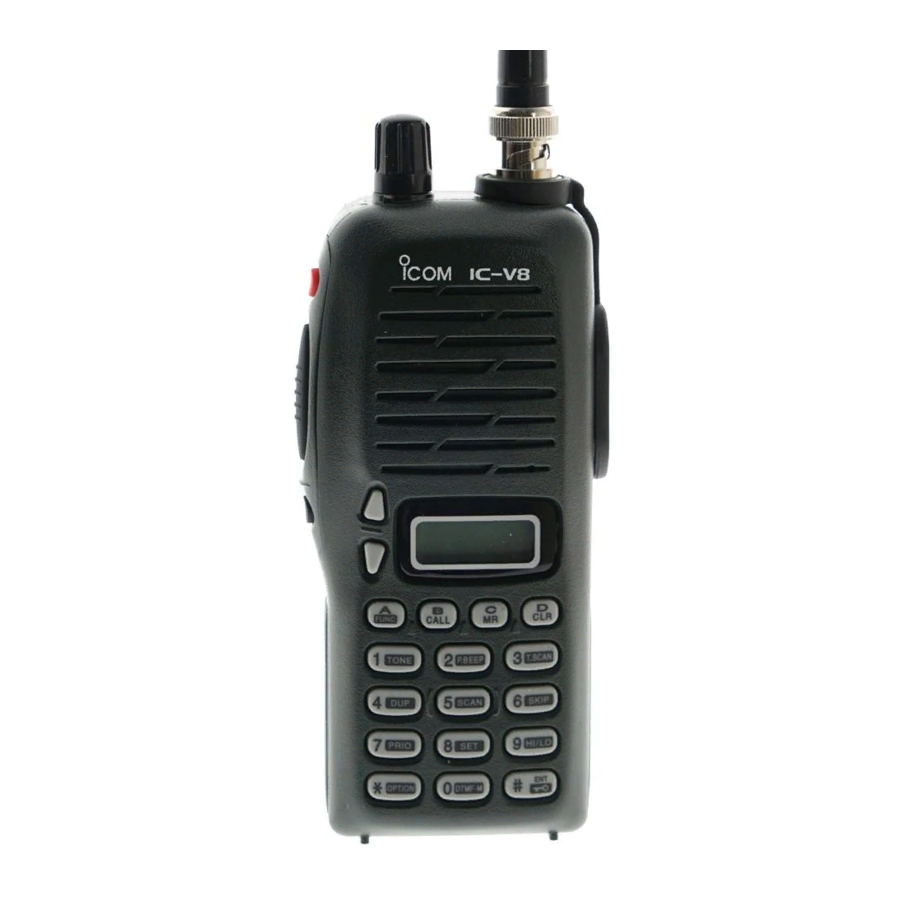
- Page 1 VHF TRANSCEIVER iC-v8...
- Page 2 INTRODUCTION This service manual describes the latest service information for the IC-V8 at the time of publication. To upgrade quality, all electrical or mechanical parts and internal circuits are subject to change without notice or oblig- ation. DANGER NEVER connect the transceiver to an AC outlet or to a DC power supply that uses more than 10.3 V.
-
Page 3: Table Of Contents
TABLE OF CONTENTS SECTION 1 SPECIFICATIONS SECTION 2 INSIDE VIEWS SECTION 3 DISASSEMBLY INSTRUCTIONS SECTION 4 CIRCUIT DESCRIPTION 4 - 1 RECEIVER CIRCUITS ....................4 - 1 4 - 2 TRANSMITTER CIRCUITS .................... 4 - 2 4 - 3 PLL CIRCUIT ........................4 - 3 4 - 4 OTHER CIRCUITS ...................... - Page 4 SECTION 1 SPECIFICATIONS ‘ ‘ GENERAL • Frequency coverage Version Receive Transmit [USA] 144.000–148.000 MHz 136.000–174.000 MHz* [GEN] 136.000–174.000 MHz* *Specifications Guaranteed: 144–148 MHz only • Type of emission : F2D/ F3E • Frequency stability : ± 10 ppm (–10˚C to +60˚C; +14˚F to +140˚F) •...
- Page 5 SECTION 2 INSIDE VIEWS TOP VIEW BOTTOM VIEW Antenna swtching circuit (D2, D8: MA77) Power amplifier (Q1: 2SK3476) Antenna swtching circuit (D1: MA77) RF amplifier (Q12: 3SK274) 1st mixer IC3A: NJM12902V (Q13: 3SK274) Q37: DTA144EU FM IF IC (IC2: TA31136FN) Crystal filter FI1, Fl3: FL-298 IF amplifier...
- Page 6 SECTION 3 DISASSEMBLY INSTRUCTIONS 3-1 DISASSEMBLY INSTRUCTION • REMOVING THE CHASSIS PANEL 1 Unscrew 1 nut A, and remove 1 knob B. 2 Unscrew 2 screws C. 3 Take off the chassis in the direction of the arrow. 4 Unplug J6 to separate front panel and chassis. (black, 2 mm) x 2 Chassis J6 (Speaker connector)
- Page 7 3-2 OPTIONAL UNIT INSTALLATIONS 1 Remove the option cover. 2 Remove the bottom protective paper of spoge. 3 Connect the UT-108 optional unit to J5. 4 Replace the option cover to the chassis-hole. Option cover Option unit SPONGE Parts name : 1556 sponge Order No.
-
Page 8: Circuit Description
SECTION 4 CIRCUIT DESCRIPTION RECEIVER CIRCUITS The 1st IF signal is applied to two crystal filters (FI1 and FI3) to suppress out-of-band signals. The filtered 1st IF signal is 4-1-1 ANTENNA SWITCHING CIRCUIT applied to the IF amplifier (Q14), then applied to the 2nd Received signals passed through the low-pass filter (L1, L2, mixer circuit (IC1, pin 16). -
Page 9: Transmitter Circuits
The AF signals are applied to the AF power amplifier circuit The audio signals (SHIFT) change the reactance of D37 to (IC5, pin 4) to obtain the specified audio level. The amplified modulate an oscillated signal at the VCO (Q50, D38). The AF signals, output from pin 10, are applied to the internal oscillated signal is amplified at the LO (Q6) and buffer (Q4) speaker (SP1) via the speaker jack (CHASSIS unit;... -
Page 10: Pll Circuit
4-5 POWER SUPPLY CIRCUITS PLL CIRCUITS VOLTAGE LINE A PLL circuit provides stable oscillation of the transmit fre- quency and receive 1st LO frequency. The PLL output com- DESCRIPTION LINE pares the phase of the divided VCO frequency to the refer- The voltage from the attached battery pack. -
Page 11: Port Allocations
4-6 PORT ALLOCATIONS 4-6-1 CPU (IC8) Port Port Description Description number name number name Input port for the clock signal from the Outputs control signal for the regulator DICK [DIAL] (S801). AFON circuit of AF power amplifier. High : When squelch is open, etc. RESET Input port for reset signal. - Page 12 4-6-2 D/A CONVERTOR IC (IC10) Port Description number name Output tunable bandpass filter control 2, 3 T1, T2 signals. • Outputs tunable bandpass filter con- trol signal while receiving. • Outputs TX power control signal while transmitting. VOLOUT Outputs AF volume control signal. Outputs DTCS’s gradient control sig- nal.
-
Page 13: Adjustment Procedures
SECTION 5 ADJUSTMENT PROCEDURES 5-1 PREPARATION REQUIRED TEST EQUIPMENT EQUIPMENT GRADE AND RANGE EQUIPMENT GRADE AND RANGE Output voltage : 7.2 V DC DC power supply Digital multimeter Input impedance : 10 M /V DC or better Current capacity : 5 A or more •... -
Page 14: Pll Adjustment
5-2 PLL ADJUSTMENT MEASUREMENT ADJUSTMENT ADJUSTMENT ADJUSTMENT CONDITIONS VALUE UNIT LOCATION UNIT ADJUST PLL LOCK 1 • Operating frequency : MAIN Connect a digital multi 2.7 V MAIN VOLTAGE 145.000 MHz meter to check point • Receiving PLL lock voltage adjustment PLL lock voltage check point... -
Page 15: Main Unit
SECTION 6 PARTS LIST [MAIN UNIT] [MAIN UNIT] ORDER ORDER DESCRIPTION DESCRIPTION 1130008350 S.IC LV2105V-TLM 6050010800 S.XTAL CR-659 (21.25 MHz) 1110003490 S.IC TA31136FN (D,EL) 6050010870 S.XTAL CR-663 (9.200 MHz) 1110005340 S.IC NJM12902V-TE1 6070000210 S.DISCRIMINATOR CDBCA450CX24 1130008090 S.IC BU4066BCFV-E1 1110001810 S.IC TA7368F (TP1) 1130010490 S.IC BR24C16FV-E2... - Page 16 [MAIN UNIT] [MAIN UNIT] ORDER ORDER DESCRIPTION DESCRIPTION 7030003400 S.RESISTOR ERJ3GEYJ 471 V (470 R238 7410000950 S.ARRAY EXB-V8V 102JV 7030003470 S.RESISTOR ERJ3GEYJ 182 V (1.8 k ) R239 7030003440 S.RESISTOR ERJ3GEYJ 102 V (1 k ) 7030003400 S.RESISTOR ERJ3GEYJ 471 V (470 R240 7030003440 S.RESISTOR ERJ3GEYJ 102 V (1 k )
- Page 17 [MAIN UNIT] [MAIN UNIT] ORDER ORDER DESCRIPTION DESCRIPTION 4030006860 S.CERAMIC C1608 JB 1H 102K-T-A C133 4030011600 S.CERAMIC C1608 JB 1C 104KT-N 4030006900 S.CERAMIC C1608 JB 1E 103K-T-A C134 4030007170 S.CERAMIC C1608 CH 1H 221J-T-A 4030007150 S.CERAMIC C1608 CH 1H 151J-T-A C135 4030011280 S.CERAMIC C1608 CH 1H 271J-T-A...
- Page 18 [MAIN UNIT] ORDER DESCRIPTION C361 4030006860 S.CERAMIC C1608 JB 1H 102K-T-A C363 4030006860 S.CERAMIC C1608 JB 1H 102K-T-A C364 4030007060 S.CERAMIC C1608 CH 1H 270J-T-A C365 4030009560 S.CERAMIC C1608 CH 1H R75B-T-A C367 4030009500 S.CERAMIC C1608 CH 1H 0R5B-T-A C368 4030009500 S.CERAMIC C1608 CH 1H 0R5B-T-A C369...
- Page 19 SECTION 7 MECHANICAL PARTS AND DISASSEMBLY [CHASSIS PARTS] [ACCESSORIES] REF. NO. ODER NO. DESCRIPTION QTY. REF. NO. ODER NO. DESCRIPTION QTY. 6510022460 Ant connector- BNC-R162 3310002840 Antenna FA-B2E 0880000840 Battery BP-208 8210017981 2251 T-front panel (B)-1 8930050890 2251 terminal holder 8930042040 1922 Belt clip 8010017990 2251 chassis 8930051290 2251 OPT sheet...
- Page 20 MP33 (C) J1 (C) MP39 (C) MP32 (C) MP32 (C) MP23 (C) MP31 (C) MP4 (C) MP3 (C) MP15 (C) MP25 (C) MP2 (C) MP5 (C) MP5 (M) MP31 (C) MP14 (C) MP8 (C) MP31 (C) MP9 (C) MP41 (C) MP37 (C) MP2 (M) MP33 (C)
- Page 21 SECTION SECTION 8 PARTS LIST SEMI-CONDUCTOR INFORMATION 8 - 1 TRANSISTORS AND FETS 8 - 2 DIODES NAME SYMBOL INSIDE VIEW NAME SYMBOL INSIDE VIEW NAME SYMBOL INSIDE VIEW DTA144EU 2SA1576 R HVC376B UN911F DTC144EU 2SB1132 Q HVU350B UN9213 MA2S077 2SC4116 GR DTC144TU 2SC4406 4...
- Page 22 SECTION 9 BOARD LAYOUTS 9 - 1 MAIN UNIT (TOP VIEW) The combination of this page and the next page shows the unit layout in the same configuration as the actual P.C. Board. BATT S801 ENCODER ANTENNA EXT. MIC EXT. SPEAKER SPEAKER 9 - 1...
- Page 23 The combination of this page and the previous page shows the unit layout in the same configuration as the actual P.C. Board. (BOTTOM VIEW) MICROPHONE OPTIONAL UNIT 9 - 2...
-
Page 24: Disassembly Information
SECTION 10 BC-146 OPTIONAL DESKTOP CHARGER INFORMATION 10-1 PARTS LIST 10-2 DISASSEMBLY INFORMATION [CHARGE UNIT] REF. NO. ODER NO. DESCRIPTION QTY. 7010007550 RESISTOR ERG3SJ680H 7010007100 RESISTOR PSD1/4V 1 k 6510021470 CONNECTOR HEC0470-01-230 5040001390 LED TLG124A 0910053820 PCB B 5650 8930051340 2338 TERMINAL 8930051340 2338 TERMINAL [CHASSIS UNIT] REF. -
Page 25: Voltage Diagram
10-3 VOLTAGE DIAGRAM C : 13.8V C : 7.2V N : 13.8V N : 13.8V R1 68 TLG124A HEC0470-01-230 C : 9.2V N : 13.8V 10-4 BOARD LAYOUT B5650 10 - 2... -
Page 26: Block Diagram
SECTION 11 BLOCK DIAGRAM X1: CR-659 21.250 MHz Q51: DTC144EU D37: MA2S077 Q59: 2SC4116 SHIFT VCO5 VCO5 REF. D1: MA77 D38: HVU350B D3: MA77 D2: MA77 OPTIONAL Q50: UMX5 Q6: 2SC4406 Q4: 2SC4406 Q3: 2SC5085 Q2:2SK3475 Q1:2SK3476 MIC, AF, PTT D4: MA77 D8: MA77 UNIT... - Page 27 SECTION 12 VOLTAGE DIAGRAM Q11 XP4601 4.68V R337 TX: 1.99V SW5V 1.8M RX: 0V PSVCO PSVCO 4.00V R362 1.45V R355 C394 CR-659 R310 R305 220k R353 OPV1 OPV1 21.250 MHz C300 4.75V 0.001 C301 2.46V 4.7k R304 C357 2SC4116 0.001 R306 C363 R311...
- Page 28 0.001 R160 EXCCL3225U R305 C289 TX: 4.06V 0.001 C288 C204 0.01 0.01 2.37V 27nH 21nH 2.7 H 2.46V RX: 0V 0.001 0.001 R304 C357 C390 C281 0.001 50nH MA77 0.001 0.001 0.96V 1.21V 17.5nH 50nH 60nH C356 0.001 0.001 150p C205 R309 8.2k C2 2.5p...
- Page 29 SECTION 12 VOLTAGE DIAGRAM Q11 XP4601 R337 4.68V TX: 1.99V SW5V 1.8M RX: 0V 0.001 R160 PSVCO PSVCO EXCCL3225U 4.00V R362 1.45V R355 C394 CR-659 OPV1 21.250 MHz 220k R353 R310 R305 C289 OPV1 C300 TX: 4.06V 0.01 0.01 0.001 C288 C204 4.75V...
- Page 30 1-1-32, Kamiminami, Hirano-ku, Osaka 547-0003, Japan Phone : 06 6793 5302 : 06 6793 0013 : http://www.icom.co.jp/world/index.html < > Corporate Headquarters Communication Equipment 2380 116th Avenue N.E., Bellevue, WA 98004, U.S.A. Himmelgeister Str. 100, D-40225 Düsseldorf, Germany Phone : ( 425 ) 454-8155...
- Page 31 Count on us! S-13802MZ-C1 1-1-32, Kamiminami, Hirano-ku, Osaka 547-0003, Japan © 2001 Icom Inc.