Table of Contents
Advertisement
Advertisement
Table of Contents

Related Manuals for Clevo M860TU

Summary of Contents for Clevo M860TU
- Page 3 Preface Notebook Computer M860TU Service Manual...
- Page 4 Preface Notice The company reserves the right to revise this publication or to change its contents without notice. Information contained herein is for reference only and does not constitute a commitment on the part of the manufacturer or any subsequent ven- dor.
-
Page 5: About This Manual
Preface About this Manual This manual is intended for service personnel who have completed sufficient training to undertake the maintenance and inspection of personal computers. It is organized to allow you to look up basic information for servicing and/or upgrading components of the M860TU se- ries notebook PC. - Page 6 Preface IMPORTANT SAFETY INSTRUCTIONS Follow basic safety precautions, including those listed below, to reduce the risk of fire, electric shock and injury to per- sons when using any electrical equipment: 1. Do not use this product near water, for example near a bath tub, wash bowl, kitchen sink or laundry tub, in a wet basement or near a swimming pool.
-
Page 7: Instructions For Care And Operation
Preface Instructions for Care and Operation The notebook computer is quite rugged, but it can be damaged. To prevent this, follow these suggestions: Don’t drop it, or expose it to shock. If the computer falls, the case and the components could be damaged. Do not expose the computer Do not place it on an unstable Do not place anything heavy... -
Page 8: Power Safety
Preface Avoid interference. Keep the computer away from high capacity transformers, electric motors, and other strong mag- netic fields. These can hinder proper performance and damage your data. Take care when using peripheral devices. Use only approved brands of Unplug the power cord before peripherals. -
Page 9: Battery Precautions
Preface Battery Precautions • Only use batteries designed for this computer. The wrong battery type may explode, leak or damage the computer. • Do not continue to use a battery that has been dropped, or that appears damaged (e.g. bent or twisted) in any way. Even if the computer continues to work with a damaged battery in place, it may cause circuit damage, which may possibly result in fire. -
Page 10: Related Documents
Preface Related Documents You may also need to consult the following manual for additional information: User’s Manual on CD This describes the notebook PC’s features and the procedures for operating the computer and its ROM-based setup pro- gram. It also describes the installation and operation of the utility programs provided with the notebook PC. VIII... -
Page 11: Table Of Contents
Preface Contents Introduction ..........1-1 Part Lists ..........A-1 Overview ..................1-1 Part List Illustration Location ............A-2 System Specifications ..............1-2 Top without Fingerprint ..............A-3 External Locator - Top View with LCD Panel Open ......1-6 Top with Fingerprint ..............A-4 External Locator - Front and Rear View .........1-7 Bottom ................... - Page 12 Preface Card Reader & 1394 JMB380 ............B-21 New Card, CCD, Fan ..............B-22 KBC-ITE IT8512 ................. B-23 HDMI, 3G ..................B-24 LED, Screw Hole ................. B-25 Azalia CODEC ALC662 .............. B-26 Audio AMP .................. B-27 SRS, MDC, BT ................B-28 DVI, INV ..................
-
Page 13: Introduction
Introduction 1: Introduction Overview This manual covers the information you need to service or upgrade the M860TU series notebook computer. Information about operating the computer (e.g. getting started, and the Setup utility) is in the User’s Manual. Information about driv- ers (e.g. -
Page 14: System Specifications
Introduction System Specifications Feature Specification Processor Types Intel® Core™2 Duo Processor 45nm (45 Nanometer) Process Technology (478-pin) Micro-FC-PGA Package, Socket P 6MB On-die L2 Cache & 1066MHz FSB (35W) T9400/ T9600 2.53GHz / 2.8GHz Intel® Core™2 Duo Processor 45nm (45 Nanometer) Process Technology (478-pin) Micro-FC-PGA Package, Socket P 6MB On-die L2 Cache &... - Page 15 Introduction Feature Specification Video Adapter NVIDIA GeForce 9600M GS PCI-E Video Card NVIDIA GeForce 8800M GTX PCI-E Video Card Options 256MB GDDR3 Video RAM On Board 512MB GDDR3 Video RAM On Board MS DirectX® 10.0 Compatible MS DirectX® 10.0 Compatible MXM-II MXM-III Supports HDCP...
- Page 16 Introduction Feature Specification I/O Ports Four USB 2.0 Ports One S/PDIF Out Jack One Combined eSATA Port/USB Port One RJ-45 LAN Jack eSATA Port (hot swapping supported in Windows Vista only): One RJ-11 Modem Jack AHCI mode supports hot swapping One Mini-IEEE1394a Port IDE mode does not support hot swapping One DC-In Jack...
- Page 17 Introduction Feature Specification Power Full Range AC/DC Adapter – AC in 100 - 240V, 50 - 60Hz DC Output 20V, 6A (120 Watts) Easy Changeable 8-Cell Smart Lithium-Ion 4400mAH Main Battery Environmental Temperature Relative Humidity Spec Operating: 5°C - 35°C Operating: 20% - 80% Non-Operating:...
-
Page 18: External Locator - Top View With Lcd Panel Open
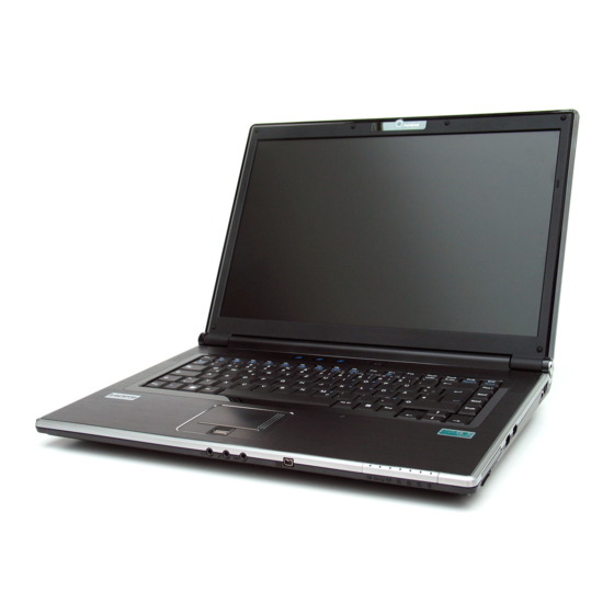
Introduction External Locator - Top View with LCD Panel Open Figure 1 Top View 1. Optional Built-In PC Camera 2. LCD 3. Hot Key Buttons 4. Power Button 5. Speakers 6. Keyboard 7. Built-In Microphone 8. TouchPad and Buttons 9. Fingerprint Reader Module (optional) 1 - 6 External Locator - Top View with LCD Panel Open... -
Page 19: External Locator - Front And Rear View
Introduction External Locator - Front and Rear View Figure 2 Front View 1. Headphone-Out Jack 2. Microphone-In Jack 3. S/PDIF-Out Jack 4. Mini-IEEE 1394 Port 5. LED Indicators Figure 3 Rear View 1. Vent/Fan Intake/ Outlet 2. DVI-Out Port 3. HDMI-Out Port 4. -
Page 20: External Locator - Left & Right Side View
Introduction External Locator - Left & Right Side View Figure 4 Left Side View 1. Optional Device Drive Bay (for CD/DVD Device) Figure 5 Right Side View 1. Express Card Slot 2. 7-in-1 Card Reader 3. 2 * USB 2.0 Ports 4. -
Page 21: External Locator - Bottom View
Introduction External Locator - Bottom View Figure 6 Bottom View 1. Vent/Fan Intake/ Outlet 2. Battery 3. Battery Release Latch 4. Component Bay Cover 5. 3.5G USIM Card Cover Overheating To prevent your com- puter from overheating make sure nothing blocks the vent/fan in- takes while the com- puter is in use. -
Page 22: Mainboard Overview - Top (Key Parts)
Introduction Mainboard Overview - Top (Key Parts) Figure 7 Mainboard Top Key Parts 1. ITE 2. Southbridge 3. CMOS Battery 4. New Card Assembly 1 - 10 Mainboard Overview - Top (Key Parts) -
Page 23: Mainboard Overview - Bottom (Key Parts)
Introduction Mainboard Overview - Bottom (Key Parts) Figure 8 Mainboard Bottom Key Parts 1. CPU Socket (no CPU installed) 2. Mini-PCIe Socket (3G Module) 3. Mini-PCIe Socket (Wireless Lan Module) 4. Memory Slots DDR2 So-DIMM 5. NorthBridge 6. 160-Pin VGA Socket Mainboard Overview - Bottom (Key Parts) 1 - 11... -
Page 24: Mainboard Overview - Top (Connectors)
Introduction Mainboard Overview - Top (Connectors) Figure 9 Mainboard Top Connectors 1. LED Cable Connector 2. Inverter Board Cable Connector 3. Keyboard Cable Connector 4. TouchPad Cable Connector 5. Microphone Cable Connector 6. CMOS Battery Connector 7. CCD Cable Connector 8. -
Page 25: Mainboard Overview - Bottom (Connectors)
Introduction Mainboard Overview - Bottom (Connectors) Figure 10 Mainboard Bottom Connectors 1. DC-In Jack 2. eSATA + USB Port 3. HDMI Port 4. DVI-Out Port 5. RJ-11 Jack 6. RJ-45 Jack 7. 7-in-1 Card Reader Connector 8. Mini-IEEE 1394a Port 9. - Page 26 Introduction 1 - 14...
-
Page 27: Disassembly
Disassembly 2: Disassembly Overview This chapter provides step-by-step instructions for disassembling the M860TU series notebook’s parts and subsystems. When it comes to reassembly, reverse the procedures (unless otherwise indicated). We suggest you completely review any procedure before you take the computer apart. Procedures such as upgrading/replacing the RAM, CD device and hard disk are included in the User’s Manual but are repeated here for your convenience. -
Page 28: Maintenance Tools
Disassembly NOTE: All disassembly procedures assume that the system is turned OFF, and disconnected from any power supply (the battery is removed too). Maintenance Tools The following tools are recommended when working on the notebook PC: • M3 Philips-head screwdriver •... -
Page 29: Maintenance Precautions
Disassembly Maintenance Precautions The following precautions are a reminder. To avoid personal injury or damage to the computer while performing a re- moval and/or replacement job, take the following precautions: Power Safety Warning 1. Don't drop it. Perform your repairs and/or upgrades on a stable surface. If the computer falls, the case and other Before you undertake components could be damaged. -
Page 30: Disassembly Steps
Disassembly Disassembly Steps The following table lists the disassembly steps, and on which page to find the related information. PLEASE PERFORM THE DISASSEMBLY STEPS IN THE ORDER INDICATED. To remove the Battery: To remove the Wireless LAN Module: 1. Remove the battery page 2 - 5 1. -
Page 31: Removing The Battery
Disassembly Removing the Battery Figure 1 Battery Removal 1. Turn the computer off, and turn it over. 2. Slide latch towards the unlock symbol and hold it in place, and lift the battery up and out of the battery bay. a. -
Page 32: Removing The Hard Disk Drive
Disassembly Removing the Hard Disk Drive Figure 2 HDD Assembly The hard disk drive is mounted in a removable case and can be taken out to accommodate other 2.5" serial (SATA) hard Removal disk drives with a height of 9.5mm (h). Follow your operating system’s installation instructions, and install all necessary drivers and utilities (as outlined in Chapter 4 of the User’s Manual) when setting up a new hard disk. - Page 33 Disassembly 6. Remove screws from the hard disk assembly. 7. Pull the hard disk assembly in the direction of the arrow 8. Carefully remove the hard disk assembly in the direction of the arrow Figure 3 9. Remove screws to separate the hard disk from the bracket and connector HDD Assembly...
-
Page 34: Removing The Optical (Cd/Dvd) Device
Disassembly Removing the Optical (CD/DVD) Device Figure 4 Optical Device 1. Turn off the computer, turn it over and remove the battery (page 2 - 5) and component bay cover (page 2 - Removal 2. Remove the screw at point , and use a screwdriver to carefully push out the optical device at point out of... -
Page 35: Removing The System Memory (Ram)
Disassembly Removing the System Memory (RAM) Figure 5 The computer has two memory sockets for 200 pin Small Outline Dual In-line Memory Modules (SO-DIMM) supporting RAM Module DDRIII (DDR3) Up to 1066 MHz. The main memory can be expanded up to 4GB. The SO-DIMM modules supported Removal are 1024MB and 2048MB DDRIII Modules. -
Page 36: Removing And Installing A Processor
Disassembly Removing and Installing a Processor Figure 6 Processor Removal Procedure Processor Removal 1. Turn off the computer, turn it over, and remove the battery (page 2 - 5) and the component bay cover (page 2 - 2. The heat sink will be visible at point on the mainboard a. - Page 37 Disassembly 5. Turn the release latch towards the unlock symbol to release the CPU. Figure 7 6. Carefully (it may be hot) lift the CPU up and out of the socket (Figure 7e). Processor Removal 7. Reverse the process to install a new CPU. (cont’d) 8.
-
Page 38: Processor Installation Procedure
Disassembly Processor Installation Procedure Figure 8 Processor 1. Insert the CPU , pay careful attention to the pin alignment, it will fit only one way (DO NOT FORCE IT!), and turn Installation the release latch towards the lock symbol (Figure 8b). -
Page 39: Removing The Vga Card
Disassembly Removing the VGA Card Figure 9 VGA Card Removal 1. Turn off the computer, turn it over, and remove the battery (page 2 - 5), the component bay cover (page 2 - 6) and the CPU heat sink (page 2 - 10). -
Page 40: Removing The 3G Module
Disassembly Removing the 3G Module Figure 10 3G Module Removal 1. Turn off the computer, turn it over, and remove the battery (page 2 - 5) and the component bay cover (page 2 - 2. The 3G module will be visible at point on the mainboard. -
Page 41: Removing The Wireless Lan Module
Disassembly Removing the Wireless LAN Module Figure 11 Wireless LAN 1. Turn off the computer, turn it over, and remove the battery (page 2 - 5) and the component bay cover (page 2 - Module Removal 2. The wireless LAN module will be visible at point on the mainboard. -
Page 42: Removing The Bluetooth Module
Disassembly Removing the Bluetooth Module Figure 12 Bluetooth Module 1. Turn off the computer, turn it over, and remove the battery (page 2 - 5) and the component bay cover (page 2 - Removal 2. The Bluetooth module will be visible at point on the mainboard. -
Page 43: Removing The Inverter Board
Disassembly Removing the Inverter Board Figure 13 Inverter Board 1. Turn off the computer, and remove the battery (page 2 - Removal 2. Remove any rubber covers, screws and hinge covers (Figure 13a), then run your finger around the middle of the frame to carefully unsnap the LCD front panel module from the back. -
Page 44: Removing The Keyboard
Disassembly Removing the Keyboard Figure 14 Keyboard Removal 1. Turn off the computer, and remove the battery (page 2 - 2. Press the four keyboard latches at the top of the keyboard to elevate the keyboard from its normal position (you a. -
Page 45: Removing The Modem
Disassembly Removing the Modem Figure 15 Modem Removal 1. Turn off the computer, turn it over and remove the battery (page 2 - 5), hard disk (page 2 - 6), optical device (page 8), RAM (page 2 - 9), CPU (page 2 - 10), VGA card (page 2 -... - Page 46 Disassembly 4. Carefully lift the top case (Figure 16e) up and off the computer. Figure 16 5. Remove screws from the modem and disconnect cable Modem Removal 6. Lift the modem Figure 16g up and off the computer. (cont’d) e. Lift the top case off the computer.
-
Page 47: Part Lists
Part Lists Appendix A:Part Lists This appendix breaks down the M860TU series notebook’s construction into a series of illustrations. The component part numbers are indicated in the tables opposite the drawings. Note: This section indicates the manufacturer’s part numbers. Your organization may use a different system, so be sure to cross-check any relevant documentation. -
Page 48: Part List Illustration Location
Part Lists Part List Illustration Location The following table indicates where to find the appropriate part list illustration. Table A - 1 Part List Illustration Part M860TU Location page A - 3 Top without Fingerprint page A - 4 Top with Fingerprint page A - 5 Bottom page A - 6... -
Page 49: Top Without Fingerprint
Part Lists Top without Fingerprint Figure A - 1 Top without Fin- gerprint 切除按鍵上方 無鉛 卡鉤加至0.8MM厚 無鉛 無鉛 無鉛 無鉛 加色粉 無鉛 無鉛 加切 理線槽 無鉛 區降 無鉛 頭徑 頭厚 圓型盤頭(無鉛) 無鉛 無鉛 無鉛 無鉛 無鉛 無鉛 無鉛 無鉛 無鉛 型... -
Page 50: Top With Fingerprint
Part Lists Top with Fingerprint Figure A - 1 Top with Finger- print 切除按鍵上方 無鉛 卡鉤加至0.8MM厚 無鉛 無鉛 無鉛 無鉛 加色粉 無鉛 無鉛 加切 理線槽 無鉛 區降 無鉛 頭徑 頭厚 圓型盤頭(無鉛) 加高 無鉛 無鉛 無鉛 無鉛 無鉛 無鉛 無鉛 無鉛 無鉛... -
Page 51: Bottom
Part Lists Bottom 無鉛 無鉛 無鉛 無鉛 無鉛 無鉛 無鉛 華力 無鉛 藍天3 互億 無鉛 無鉛 無鉛 無鉛 無鉛 凱碩 無鉛 Figure A - 2 無鉛 無鉛 Bottom 無鉛 無鉛 無鉛 無鉛 無鉛 無鉛 (三價絡)無鉛 無鉛 無鉛 無鉛 海華 無鉛 無鉛... -
Page 52: Lcd
Part Lists Figure A - 3 無鉛 無鉛 無鉛 (加背膠) 無鉛 (無印刷) 加背膠 無鉛 無鉛 無鉛 水電鍍 無鉛 (非耐落) 無鉛 無鉛 無鉛 無鉛 無鉛 無鉛 無鉛 無鉛 無鉛 無鉛 無鉛 惠貿 無鉛 無鉛 無鉛 無鉛 無鉛 無鉛 無鉛 無鉛 無鉛 無鉛... -
Page 53: Dvd-Rom Drive
Part Lists DVD-ROM Drive Figure A - 4 DVD-ROM Drive 無鉛 無鉛 無鉛 無鉛 無鉛 DVD-ROM Drive A - 7... -
Page 54: Combo Drive
Part Lists Combo Drive Figure A - 5 Combo Drive 無鉛 無鉛 無鉛 無鉛 A - 8 Combo Drive... -
Page 55: Hdd
Part Lists Figure A - 6 無鉛 (無鉛) HDD A - 9... - Page 56 Part Lists A - 10...
-
Page 57: Schematic Diagrams
Schematic Diagrams Appendix B:Schematic Diagrams This appendix has circuit diagrams of the M860TU notebook’s PCB’s. The following table indicates where to find the appropriate schematic diagram. Table B - 1 Diagram - Page Diagram - Page Diagram - Page Schematic SYSTEM BLOCK DIAGRAM - Page B - 2 ICH9-M 4/4, Power - Page B - 17 Power 1.5V/0.75V - Page B - 32... - Page 58 Schematic Diagrams SYSTEM BLOCK DIAGRAM CLEVO M860TU System Block Diagram BU TT OM BO AR D SY S5 V,S YS 3V ,V DD3 ,V DD 5, 3V ,5V B OTT OM P OWE R BO TT OM LE D M EM ORY T ER MI NA TIO NS...
- Page 59 Schematic Diagrams Penryn 1/2 U 2 2 A U 2 2 B H _ A # [ 3 5: 3 ] H _ A # 3 A [ 3 ] # A D S # H _ A D S # H _ D # [ 63 : 0 ] H _ D # [ 6 3 : 0] H _ A # 4...
- Page 60 Schematic Diagrams Penryn 2/2 V C O R E V C O R E U 2 2 D PLA CE NE AR CP U U 2 2 C V S S [ 00 1 ] V S S [ 0 8 2] V C OR E A B 2 0 P 21...
- Page 61 Schematic Diagrams Cantiga 1/6, Host P in N a m e S tr ap Description C o nfigur ation 000 = 10 66 010 = 80 0 C FG2: 0 FS B Fr eguency 011 = 66 7 U 2 5 A O t hers = R ese rved H _A #[ 3 5 : 3 ] 2 A 1 4...
-
Page 62: Cantiga 2/6, Peg
Schematic Diagrams Cantiga 2/6, PEG D MI X2 se lect P E G_ TX P [ 0. . 1 5] P E G_T X P [ 0 . . 1 5] P E G_ TX N [ 0 . . 15 ] P E G_T X N [ 0. -
Page 63: Cantiga 3/6, Ddr
Schematic Diagrams Cantiga 3/6, DDR U25E M _B_D Q[63:0] U25D M _B _DQ0 A K47 B C16 M _A _DQ [ 6 3: 0] S B_D Q_0 SB _B S _0 M _B _B S 0# 11 M _A_D Q0 A J38 B D21 M _B _DQ1... -
Page 64: Cantiga 4/6, Power 1
Schematic Diagrams Cantiga 4/6, Power 1 U 2 5 G 1 . 5 V 1. 5V _G MC H V GF X_ C OR E 1 . 0 5 V M U 2 5 F V C C _ G MC H A P 33 W 28 V C C _ S M_ 1... -
Page 65: Cantiga 5/6, Gnd
Schematic Diagrams Cantiga 5/6, GND U25I U25J AU48 AM 36 BG 21 VS S_1 VS S_100 VSS _199 VS S_297 AR48 AE36 VS S_2 VS S_101 VSS _200 VS S_298 AL48 AW 21 VS S_3 VS S_102 VSS _201 VS S_299 B B47 AU21 VS S_4... -
Page 66: Cantiga 6/6, Power 2
Schematic Diagrams Cantiga 6/6, Power 2 1 . 0 5V S U 2 5 H + V C C P _ GMC H L4 1 1 . 0 5V M 1. 0 5 V M For P M H C B 16 0 8K F -12 1 T2 5 852 mA 3 . -
Page 67: Ddr3 So-Dimm 1
Schematic Diagrams DDR3 SO-DIMM 1 SO-DIMM 0 J D I M M1 A M _A _A [ 14 : 0 ] M_ A _ D Q [ 63 : 0 ] 6 M _A _ A 0 M _A _D Q0 D Q0 M _A _ A 1 M _A _D Q1... -
Page 68: Ddr3 So-Dimm 2
Schematic Diagrams DDR3 SO-DIMM 2 SO-DIMM 1 J D I MM 2A M_ B _ A [ 14 : 0 ] M_ B _ D Q [ 6 3: 0] 6 M_ B _ A 0 M_ B _ D Q 0 D Q0 M_ B _ A 1 M_ B _ D Q 1... -
Page 69: Lcd
Schematic Diagrams 1. 8 V S 1 . 8V S PANEL V D D 1 V D D 1 V D D 2 V D D 2 V D D 3 V D D 3 V D D 4 V D D 4 V D D 5 V D D 5 V D D 6... -
Page 70: Ich9-M 1/4, Sata
Schematic Diagrams ICH9-M 1/4, SATA D VT:Change to 12P R TC V C C C 2 6 8 1 2 p_ 5 0V _0 4 20m i ls R 1 7 5 V D D 3 C 5 66 C 55 9 1 0M _0 4 3 2 . -
Page 71: Ich9-M 2/4, Pci, Usb
Schematic Diagrams ICH9-M 2/4, PCI, USB G NT0 #0 an d S PI_CS# 1 h ave S P I_MO SI have a wea k inter nal U 1 5D pul l - down PCI E xp res s Por t Con fi gu rat io n 2 b it 2 in ter na l pu ll u p. -
Page 72: Ich9-M 3/4
Schematic Diagrams ICH9-M 3/4 3 . 3 V S U 1 5C 3 . 3 V I C H _ S MB C L K 0 G1 6 A H 2 3 S A T A 0 GP 1 0 , 11 , 1 8 I C H _S MB C L K 0 S MB C LK S A TA 0 G P / GP I O 21... -
Page 73: Ich9-M 4/4, Power
Schematic Diagrams ICH9-M 4/4, Power R T C V C C U 1 5 F U 1 5E 20m ils 1 . 0 5V S A 2 3 A 1 5 Z 1 6 07 A A 2 6 L ayout not e: V C C R T C V C C 1 _0 5 [ 1 ] V S S [ 1 ]... -
Page 74: Odd, Usb2.0 & Esata
Schematic Diagrams ODD, USB2.0 & eSATA S A T A TX N 4 LP 1 4 E S A T A _T X N EM I S A T A TX P 4 E S A T A _T X P Co -La yo ut USB 2.0&... -
Page 75: Clock Generator
Schematic Diagrams Clock Generator CR# A: CLOCK GENERATOR 3 . 3V M CR# B: C LK _ MC H _ B C L K C 5 03 *1 0p _ N P O _0 4 CR# C: 3 . 3 V M_ C L K CR# D: L 47 L ayou t no te:... -
Page 76: Pci-E Lan Rtl8111C, Rj45Rj11
Schematic Diagrams PCI-E LAN RTL8111C, RJ45RJ11 L5 6 3 . 3V P VT: F or C le vo N or ma l De si gn G LA N 3 3 L A N _ V D D 3 L A N V D D 1 2 H C B 2 0 12 K F - 50 0 T 40 S 1 2 60 mi l... -
Page 77: Card Reader & 1394 Jmb380
Schematic Diagrams Card Reader & 1394 JMB380 IEEE1394 13 9 4_ T P B I A S 0 C 6 6 8 0 . 33 u _1 6 V _ 06 SD Car d MS Ca rd LP 5 R 5 08 5 6 _0 4 J1 3 94 P O R T 1 M DIO 0... -
Page 78: New Card, Ccd, Fan
Schematic Diagrams New Card, CCD, Fan NEW CARD 3. 3 V C 3 4 0 P VT 3 , 9, 1 3 , 16 , 2 3 , 33 , 3 6 1 . 5 V S *. 1 u _1 6 V _ 04 3 . -
Page 79: Kbc-Ite It8512
Schematic Diagrams KBC-ITE IT8512 R 3 11 1 0K _0 4 W D T _ E N V D D 3 V D D 3 K B C _ A V D D L 3 9 V D D 3 F C M1 6 0 8K -1 2 1T 0 6 R 3 12 *1 0 K _ 04... -
Page 80: Hdmi, 3G
Schematic Diagrams HDMI, 3G 5 V S _ H D MI 3. 3 V S HDMI 5 V S R 67 6 R 67 7 D V T R 6 78 R 6 79 3 . 9K _ 0 4 3 . -
Page 81: Led, Screw Hole
Schematic Diagrams LED, Screw Hole ACIN BATT V D D 3 V D D 3 3 . 3 V S PWR/SUS CHARGE FULL R 6 3 2 R 6 2 8 R 6 34 R 62 6 R 62 4 R 62 3 R 6 22 1 0 0 _0 6... -
Page 82: Azalia Codec Alc662
Schematic Diagrams Azalia CODEC ALC662 3 . 3 V S 5 V S _ A U D 5 V S L 59 L2 4 Z 2 5 01 H C B 1 6 08 K F -1 2 1T 2 5 H C B 1 6 08 K F -1 2 1T 2 5 C 70 5 C 3 54... -
Page 83: Audio Amp
Schematic Diagrams Audio AMP 5 V S _ A M P 5 V S L2 3 H C B 2 0 1 2 K F -5 0 0 T 4 0 3 . 3 V S 5 V S C 3 57 C 3 8 4 C 3 82 C 38 1... -
Page 84: Srs, Mdc, Bt
Schematic Diagrams SRS, MDC, BT AUDIO PROCESSOR PRE-AMP 5V S _A U D 2 , 14 , 1 5, 1 6 , 1 9, 2 1 , 28 , 2 9 , 30 , 3 1, 3 2 , 3 4, 3 6 , 37 , 3 8 3. -
Page 85: Dvi, Inv
Schematic Diagrams DVI, INV 3. 3 V S 3 . 3 V S C 1 7 C 1 6 C 1 8 * . 1u _ 16 V _ 0 4 * . 1u _ 1 6V _ 0 4 * 1 u_ 1 0V _0 6 B A V 9 9 B A V 99... -
Page 86: Power Charger, Dc-In
Schematic Diagrams Power Charger, DC-In V A + + D V T P F B 1 7 A / 1 2 5V J B A T T A 1 4. 7 u _2 5 V _ 08 V D D 3 Z 2 90 2 J A C B 1 4 . -
Page 87: Power Gpu
Schematic Diagrams Power GPU V I N V I N Near N B N ear S B P C 1 64 P C 1 65 P C 16 1 P D 2 P C 1 5 8 P C 15 9 P C 16 0 P C 23 1 P C 2 39... -
Page 88: Power 1.5V/0.75V
Schematic Diagrams Power 1.5V/0.75V V I N 3 . 3 V V D D Q P R 1 9 9 P R 1 9 3 P D 2 4 F M0 5 4 0 -N P R 20 4 1 . 5 M_ 0 4 1 0 _ 0 4 6- 06 -00 54 0-0 21 1 00 K _ 0 4... -
Page 89: Power 3.3Vm/1.8Vs/1.05Vm
Schematic Diagrams Power 3.3VM/1.8VS/1.05VM V I N P C 5 0 P C 5 1 P C 52 Z 3 2 01 P C 46 P C 4 7 P C 4 8 P R 1 7 9 * 10 m i l _ s ho rt P R 1 6 1 1 0 _ 04 Z 32 1 0... -
Page 90: Power 3Vs/5Vs / Power S/W
Schematic Diagrams Power 3VS/5VS / Power S/W POWER SW P ower Pl ane 6 -15 -044 68-7 B0 S Y S 15 V V D D 5 5V S P Q 29 V I N 1 P D 3 S C S 75 1 V -40 P R 1 9 1 V I N 6-06 -75 140- 061... -
Page 91: Power Vdd3/Vdd5/3.3V/5V
Schematic Diagrams Power VDD3/VDD5/3.3V/5V P Q3 4 V I N Pow er P lane A O4 4 6 8 Powe r Pl ane 6-15 -044 68- 7B0 V D D 5 P Q1 8 A O4 46 8 S Y S 1 5V V D D 3 3 . -
Page 92: Power Vcore
Schematic Diagrams Power VCORE VCORE FOR MEROM CPU V I N V -R C 1 P C 1 0 9 P C 10 3 P D 1 1 1 u _ 2 5V _ 0 8 F M0 5 4 0-N P R 1 13 EMI:cl ose to PQ37 1 0 00 p _ 50 V _ 0 4... -
Page 93: Mini Card/Wlan
Schematic Diagrams Mini Card/WLAN MINI-PCIE CARD W LA N 1_ 3 . 3 V JM I N I _ W L A N 1 P C I E _W A K E # 1 5 , 19 , 2 1, 22 , 2 3 P C I E _ W A K E # W A K E # 3. -
Page 94: Mxm Pci-E Type Iii
Schematic Diagrams MXM PCI-E Type III JM X M1 1V 8R U N 2 V 5 R U N V I N P WR _S R C C 123 C 124 C 2 3 C 24 C 25 C 4 67 C 477 1 V 8 R U N P W R _ S R C... -
Page 95: Board To Board Con/Tpm
Schematic Diagrams Board to Board CON/TPM HOT KEY (M/B side) P Q6 6 2 N 7 00 2 D D ON # P Q 67 2 N 7 0 0 2 JL E D 2 M _ B T N # 3 3 A P _K E Y # W E B 0# W E B 1 #... -
Page 96: Button Board
Schematic Diagrams Button Board BJLED 2 BJ SPK1 BPW RBTN# B+5VS BW EB#0 BSPKOUTR+ BW EB#1 BSPKOUTR- BW EB#2 BSPKOUTL+ BSPKOUTL- B +5VS B +VI N 680_06 88266-0400 BSPKOUTR+ BC 7 BC10 Z3901 BSPKOUTR- *180P_04 *180P_04 BSPKOUTL+ POWE R BSPKOUTL- BUTT ON HT-150N B-D T B+VI N... -
Page 97: Click Board
Schematic Diagrams Click Board T 3 . 3V T +5 V S TM39 8 T H 3 T H 1 T H 4 T H 6 TJ _ TP B 2 C 23 6 D 8 7 C 23 6 D 8 7 C 23 6 D 8 7 C 23 6 D 8 7 T R 9... -
Page 98: Finger Printer Board
Schematic Diagrams Finger Printer Board FU 1 FES D _R IN G E XT_R I N G2 FGR I D 0/S EN S E C R I D O R I N G F GN D FMU XOU T MU XOU T A VD D F AV D D Sheet 41 of 42... -
Page 99: Sim Card Board
Schematic Diagrams SIM Card Board Sheet 42 of 42 SIM Card Board MR 3 *4. 7K _04 MJ _SI MT1 LOCK (TOP VIEW) MJ _ST1 MUI M_C LK *10m il_s hor t MR 2 * 10m il_s hor t MU IM_D ATA U I M_CLK U I M_D A TA MUI M_R ST... - Page 100 Schematic Diagrams B - 44...