Table of Contents
Advertisement
Quick Links
Advertisement
Table of Contents
Troubleshooting

Related Manuals for Panasonic KX-TG6500BXB


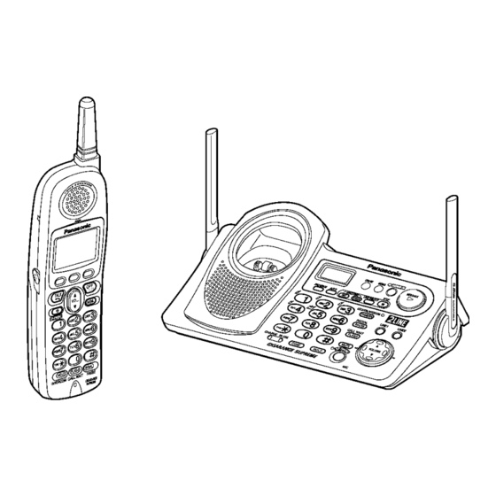
Summary of Contents for Panasonic KX-TG6500BXB
- Page 1 ORDER NO. KM40406474C3 Telephone Equipment KX-TG6500BXB KX-TGA650BXB Expandable Cordless Answering System Black Version (for Asia, Middle Near East and other areas) © 2004 Panasonic Communications Co., Ltd. All rights reserved. Unauthorized copying distribution is a violation of law.
-
Page 2: Table Of Contents
KX-TG6500BXB / KX-TGA650BXB Note: Because CONTENTS 5 to 10 are the extracts from the Operating Instructions of this model, they are subject to change without notice. Please refer to the original Operating Instructions for further information. CONTENTS Page Page 1 ABOUT LEAD FREE SOLDER (PbF: Pb free) 9.6. - Page 3 KX-TG6500BXB / KX-TGA650BXB 16.2. To Terminate Communication 29.3. Removing Solder from Between Pins 16.3. Ringing 30 CABINET AND ELECTRICAL PARTS (BASE UNIT) 17 BLOCK DIAGRAM (BASE UNIT_MAIN) 31 CABINET AND ELECTRICAL PARTS (HANDSET) 18 CIRCUIT OPERATION (BASE UNIT_MAIN) 32 CABINET AND ELECTRICAL PARTS (CHARGER UNIT) 18.1.
-
Page 4: About Lead Free Solder (Pbf: Pb Free)
KX-TG6500BXB / KX-TGA650BXB 1 ABOUT LEAD FREE SOLDER (PbF: Pb free) Note: In the information below, Pb, the symbol for lead in the periodic table of elements, will refer to standard solder or solder that contains lead. We will use PbF when discussing the lead free solder used in our manufacturing process which is made from Tin (Sn), Silver (Ag), and Copper (Cu). -
Page 5: How To Recognize That Pb Free Solder Is Used
KX-TG6500BXB / KX-TGA650BXB 1.2. How to recognize that Pb Free solder is used 1.2.1. Base Unit 1.2.1.1. Main P.C.B. IC501 IC601 IC701 Marked (Component View) Marked (Flow Solder Side View) Note: The location of the “PbF” mark is subject to change without notice. - Page 6 KX-TG6500BXB / KX-TGA650BXB 1.2.1.2. Operational P.C.B. CN963 LCD900 Marked (Component View) Marked (Flow Solder Side View) Note: The location of the “PbF” mark is subject to change without notice.
- Page 7 KX-TG6500BXB / KX-TGA650BXB 1.2.2. Handset 1.2.2.1. Main P.C.B. Marked IC202 IC201 IC701 (Component View) Marked (Flow Solder Side View) Note: The location of the “PbF” mark is subject to change without notice. 1.2.3. Charger Unit Marked (Flow Solder Side View) Note: The location of the “PbF”...
-
Page 8: For Service Technicians
KX-TG6500BXB / KX-TGA650BXB 2 FOR SERVICE TECHNICIANS ICs and LSIs are vulnerable to static electricity. When repairing, the following precautions will help prevent recurring malfunctions. 1. Cover plastic parts boxes with aluminum foil. 2. Ground the soldering irons. 3. Use a conductive mat on worktable. -
Page 9: Battery
KX-TG6500BXB / KX-TGA650BXB 5 BATTERY 5.1. Installing the Battery in the Handset 5.2. Battery Charge 5.3. Battery Recharge Note for service: The battery strength may not be indicated correctly if the battery is disconnected and connected again, even after it is fully... -
Page 10: Battery Strength
KX-TG6500BXB / KX-TGA650BXB 5.4. Battery Strength 5.5. Battery Replacement 5.6. Battery Information... -
Page 11: Location Of Controls
KX-TG6500BXB / KX-TGA650BXB 6 LOCATION OF CONTROLS 6.1. Base Unit... -
Page 12: Handset
KX-TG6500BXB / KX-TGA650BXB 6.2. Handset 6.3. Charger Unit... -
Page 13: How To Use The Soft Keys/Navigator Keys
KX-TG6500BXB / KX-TGA650BXB 6.4. How to Use the Soft Keys/Navigator Keys... -
Page 14: Displays
KX-TG6500BXB / KX-TGA650BXB 7 DISPLAYS 7.1. Handset Display and Base Unit Display... - Page 15 KX-TG6500BXB / KX-TGA650BXB...
-
Page 16: Troubleshooting (Handset Lcd)
KX-TG6500BXB / KX-TGA650BXB 7.2. Troubleshooting (Handset LCD) - Page 17 KX-TG6500BXB / KX-TGA650BXB Cross Reference: Erasing an Item in the Phone Book (P.46). Canceling the Handset Registration (P.64).
-
Page 18: Settings
KX-TG6500BXB / KX-TGA650BXB 8 SETTINGS 8.1. Connections 8.1.1. Connecting the AC Adaptor... - Page 19 KX-TG6500BXB / KX-TGA650BXB 8.1.2. Connecting the Telephone Line Cord...
- Page 20 KX-TG6500BXB / KX-TGA650BXB...
- Page 21 KX-TG6500BXB / KX-TGA650BXB...
- Page 22 KX-TG6500BXB / KX-TGA650BXB 8.1.3. Connecting an Optional Headset...
-
Page 23: Function Menu Table
KX-TG6500BXB / KX-TGA650BXB 8.2. Function Menu Table... -
Page 24: Date And Time
KX-TG6500BXB / KX-TGA650BXB 8.3. Date and Time... -
Page 25: Dialing Mode
KX-TG6500BXB / KX-TGA650BXB 8.4. Dialing Mode 8.5. Line Mode... -
Page 26: Voice Enhancer Technology
KX-TG6500BXB / KX-TGA650BXB 8.6. Voice Enhancer Technology... -
Page 27: Ringer Tone
KX-TG6500BXB / KX-TGA650BXB 8.7. Ringer Tone 8.7.1. Handset Ringer Tone... - Page 28 KX-TG6500BXB / KX-TGA650BXB 8.7.2. Base Unit Ringer Tone (Use Either the Base Unit or the Handset) Cross Reference: Handset Ringer Tone (P.27).
-
Page 29: Direct Commands
KX-TG6500BXB / KX-TGA650BXB 8.8. Direct Commands Cross Reference: Date and Time (P.24). To Copy One Phone Book Item to Another Handset (P.47). To Copy All of the Items in Your Phone Book to Another Handset (P.47). Remote Code (P.39). - Page 30 KX-TG6500BXB / KX-TGA650BXB Cross Reference: Re-registering the Handset (P.65). Storing Names and Numbers (P.42). Dialing from the Phone Book (P.44).
-
Page 31: Operations
KX-TG6500BXB / KX-TGA650BXB 9 OPERATIONS 9.1. Answering System 9.1.1. Greeting Message... - Page 32 KX-TG6500BXB / KX-TGA650BXB...
- Page 33 KX-TG6500BXB / KX-TGA650BXB 9.1.2. Caller’s Recording Time 9.1.3. Message Alert...
- Page 34 KX-TG6500BXB / KX-TGA650BXB 9.1.4. Erasing Messages...
-
Page 35: For Call Waiting Service Users
KX-TG6500BXB / KX-TGA650BXB 9.2. For Call Waiting Service Users... -
Page 36: Using The Pause Button (For Pbx Line/Long Distance Calls)
KX-TG6500BXB / KX-TGA650BXB 9.3. Using the PAUSE Button (For PBX Line/Long Distance Calls) 9.4. FLASH Button... -
Page 37: Line Selection
KX-TG6500BXB / KX-TGA650BXB 9.5. Line Selection 9.5.1. Handset Line Selection 9.5.2. Base Unit line selection... -
Page 38: Remote Operation From A Touch Tone Phone
KX-TG6500BXB / KX-TGA650BXB 9.6. Remote Operation from a Touch Tone Phone Cross Reference: Direct Remote Operation (P.41). - Page 39 KX-TG6500BXB / KX-TGA650BXB 9.6.1. Remote Code...
- Page 40 KX-TG6500BXB / KX-TGA650BXB 9.6.2. Voice Menu...
- Page 41 KX-TG6500BXB / KX-TGA650BXB 9.6.3. Direct Remote Operation...
-
Page 42: Phone Book
KX-TG6500BXB / KX-TGA650BXB 9.7. Phone Book 9.7.1. Storing Names and Numbers Cross Reference: Chain Dial (P.45). - Page 43 KX-TG6500BXB / KX-TGA650BXB...
- Page 44 KX-TG6500BXB / KX-TGA650BXB 9.7.2. Dialing from the Phone Book...
- Page 45 KX-TG6500BXB / KX-TGA650BXB 9.7.3. Chain Dial Cross Reference: Dialing from the Phone Book (P.44).
- Page 46 KX-TG6500BXB / KX-TGA650BXB 9.7.4. Editing an Item in the Phone Book Cross Reference: Dialing from the Phone Book (P.44). 9.7.5. Erasing an Item in the Phone Book Cross Reference: Dialing from the Phone Book (P.44). 9.7.6. Copying Items in the Phone Book (When the System Has 2 or More Handsets)
- Page 47 KX-TG6500BXB / KX-TGA650BXB 9.7.6.1. To Copy One Phone Book Item to Another Handset Cross Reference: Dialing from the Phone Book (P.44). 9.7.6.2. To Copy All of the Items in Your Phone Book to Another Handset...
-
Page 48: Troubleshooting
KX-TG6500BXB / KX-TGA650BXB 10 TROUBLESHOOTING Cross Reference: (*1) Troubleshooting (Handset LCD) (P.16). (*2) Re-registering the Handset (P.65). (*3) Battery Charge (P.9). - Page 49 KX-TG6500BXB / KX-TGA650BXB Cross Reference: (*4) Using the PAUSE Button (For PBX Line/Long Distance Calls) (P.36). (*5) Message Alert (P.33). (*6) Connecting an Optional Headset (P.22).
- Page 50 KX-TG6500BXB / KX-TGA650BXB Cross Reference: (*7) Caller’s Recording Time (P.33). (*8) Erasing Messages (P.34). (*9) Remote Code (P.39). (*10) Date and Time (P.24).
- Page 51 KX-TG6500BXB / KX-TGA650BXB Cross Reference: (*11) BATTERY (P.9). (*12) Connections (P.18). (*13) Dialing Mode (P.25). (*14) Battery Recharge (P.9). (*15) Installing the Battery in the Handset (P.9). (*16) Date and Time (P.24).
-
Page 52: Disassembly Instructions
KX-TG6500BXB / KX-TGA650BXB 11 DISASSEMBLY INSTRUCTIONS 11.1. Base Unit Shown in Fig.- To Remove - Remove - Cabinet Cover Screws (2.6 × 12)..(A) × 5 Main P.C. Board Tape and Solder Cables Main P.C. Board Operational P.C. Board Tape Screws (2.6 × 8)...(B) × 10... -
Page 53: Handset
KX-TG6500BXB / KX-TGA650BXB 11.2. Handset Shown in Fig.- To Remove - Remove - Cabinet Cover Screws (2.6 × 12)..(C) × 2 Follow the procedure. Main P.C. Board Tape and Solder Screw (2.6 × 12)..(D) × 1 Screws (2.6 × 8)..(E) × 2 Charge Terminals Main P.C. -
Page 54: Charger Unit
KX-TG6500BXB / KX-TGA650BXB 11.3. Charger Unit Shown in Fig.- To Remove - Remove - Cabinet Cover Screws (2.6 × 12)..(F) × 1 Main P.C.Board Main P.C.Board... -
Page 55: Assembly Instructions
KX-TG6500BXB / KX-TGA650BXB 12 ASSEMBLY INSTRUCTIONS 12.1. Fix the LCD to the Main P.C. Board (Handset) -
Page 56: Troubleshooting Guide
KX-TG6500BXB / KX-TGA650BXB 13 TROUBLESHOOTING GUIDE FLOW CHART Cross Reference: Note: Check Power (P.57) (*1) When a user claims that the unit disconnects a call right after the greeting message and no incoming messages can Error Message Table (P.57) be recorded, this symptom can not be reappeared with TEL Check Sp-phone Transmission (P.58) -
Page 57: Check Power
KX-TG6500BXB / KX-TGA650BXB 13.1. Check Power BASE UNIT Cross Reference: Note: Power Supply Circuit (P.93) Flash Memory is IC601. Reset Circuit (P.95) DSP is IC501. 13.2. Error Message Table Display Symptom Remedy The initialization was tried, but it could not be done. -
Page 58: Check Sp-Phone Transmission
KX-TG6500BXB / KX-TGA650BXB 13.3. Check Sp-phone Transmission BASE UNIT Cross Reference: Note: SIGNAL ROUTE (P.116) Flash Memory is IC601. Telephone Line Interface (P.96) DSP is IC501. 13.4. Check Sp-phone Reception BASE UNIT Cross Reference: Note: Telephone Line Interface (P.96) Flash Memory is IC601. -
Page 59: Check Recording
KX-TG6500BXB / KX-TGA650BXB 13.5. Check Recording BASE UNIT a) Not record Greeting Message b) Not record Incoming Message c) How to change the Auto Disconnect activation (time) Some Telephone Company lines (fiber or cable) ON Hook and OFF Hook voltages are lower than conventional lines, which may cause a malfunction of Auto Disconnect detection.To solve this problem, try changing the Auto Disconnect activation (time) -
Page 60: Check Playback
KX-TG6500BXB / KX-TGA650BXB 13.6. Check Playback BASE UNIT Cross Reference: Note: Power Supply Circuit (P.93) Flash Memory is IC601. DSP is IC501. -
Page 61: Check Battery Charge
KX-TG6500BXB / KX-TGA650BXB 13.7. Check Battery Charge BASE UNIT CHARGER UNIT Note: Flash Memory is IC601. DSP is IC501. HANDSET... -
Page 62: Check Link
KX-TG6500BXB / KX-TGA650BXB 13.8. Check Link BASE UNIT HANDSET Note: Flash Memory is IC601. DSP is IC501. Cross Reference: Check the RF part (P.63) (*1) Refer to Finding out the Defective part (P.63). -
Page 63: Check The Rf Part
KX-TG6500BXB / KX-TGA650BXB 13.9. Check the RF part 13.9.1. Finding out the Defective part After All the Checkings or Repairing 1. After all the checkings or repairing, cancel the Registration of Regular HS to checked Base Unit, and checked Handset to Regular BU. - Page 64 KX-TG6500BXB / KX-TGA650BXB 13.9.1.1. Canceling the Handset Registration Cross Reference: Re-registering the Handset (P.65)
- Page 65 KX-TG6500BXB / KX-TGA650BXB 13.9.1.2. Re-registering the Handset...
- Page 66 KX-TG6500BXB / KX-TGA650BXB 13.9.2. RF Check Flowchart Each item (1 ~ 6) of RF Check Flowchart corresponds to Check Table for RF part (P.67). Please refer to the each item.
- Page 67 KX-TG6500BXB / KX-TGA650BXB 13.9.3. Check Table for RF part Item BU (Base Unit) Check HS (HandSet) Check Link Confirmation Normal 1. Register Regular HS to BU (to be checked). 1. Register HS (to be checked) to Regular BU. 2. Press [Talk] key of the Regular HS to 2.
- Page 68 KX-TG6500BXB / KX-TGA650BXB 13.9.4. TEST RANGE Check Circuit block which range is defective can be found by the following check. Item BU (Base Unit) Check HS (HandSet) Check Range Confirmation TX 1. Register Regular HS to BU (to be checked).
- Page 69 KX-TG6500BXB / KX-TGA650BXB 13.9.5. RF-DSP Interface Signal Wave Form <Test Burst Mode>...
- Page 70 KX-TG6500BXB / KX-TGA650BXB <Test Burst Mode>...
-
Page 71: Check Handset Voice Transmission
KX-TG6500BXB / KX-TGA650BXB 13.10. Check Handset Voice Transmission Cross Reference: SIGNAL ROUTE (P.116) 13.11. Check Handset Voice Reception Cross Reference: SIGNAL ROUTE (P.116) Note: When checking the RF part, Refer to Check the RF part (P.63) 13.12. Check Caller ID... -
Page 72: Adjustment And Test Mode
KX-TG6500BXB / KX-TGA650BXB 14 ADJUSTMENT AND TEST MODE 14.1. Test Mode Flow Chart for Base Unit 14.1.1. Test Burst Mode Note: (*1) LCD displays the Channel number. - Page 73 KX-TG6500BXB / KX-TGA650BXB 14.1.2. RX-CW TEST Mode Note: (*1) LCD displays the Channel number.
- Page 74 KX-TG6500BXB / KX-TGA650BXB 14.1.3. Test Link Mode Note: (*1) LCD displays the Channel number. (*2) LCD displays the number of selected power.
- Page 75 KX-TG6500BXB / KX-TGA650BXB 14.1.4. Adjustment Mode Cross Reference Check and Adjust X501 (Base Unit) Frequency (P.80) Note: (*1) This is an adjustment value (hex.).
-
Page 76: Test Mode Flow Chart For Handset
KX-TG6500BXB / KX-TGA650BXB 14.2. Test Mode Flow Chart for Handset 14.2.1. Test Burst Mode Note: (*1) LCD displays the Channel number. (exception: default/ CH00 = 1ch.) - Page 77 KX-TG6500BXB / KX-TGA650BXB 14.2.2. RX-CW TEST Mode Note: (*1) LCD displays the Channel number. (exception: default/ CH00 = 1ch.)
- Page 78 KX-TG6500BXB / KX-TGA650BXB 14.2.3. Test Link Mode Note: (*1) LCD displays the Channel number. (exception: default/ CH00 = 1ch.) (*2) for factory use only...
- Page 79 KX-TG6500BXB / KX-TGA650BXB 14.2.4. Adjustment Mode Cross Reference (*1) Adjust Battery Low Detector Voltage (Handset) (P.80) Note: (*2) These are the default values. (*3) These values may not be fixed depending on the battery strength.
-
Page 80: X501 (Base Unit), X201 (Handset) Check
KX-TG6500BXB / KX-TGA650BXB 14.3. X501 (Base Unit), X201 (Handset) Check Equipment: Frequency counter Check Point for measurement: Q521 collector (Base Unit)/BCK (Handset) Checking tolerance: 13.824MHz ± 270Hz (Base Unit)/13.824MHz ± 100Hz (Handset) 14.3.1. Check and Adjust X501 (Base Unit) Frequency 1. -
Page 81: Base Unit Reference Drawing
KX-TG6500BXB / KX-TGA650BXB Q236 Q261 D201 Q241 DA214 PC241 DA213 Q256 L202 Q245 P201 SA201 Q136 DA114 L201 DA113 Q156 Q271 P101 SA101 Q855 Q891 FL861 Q875 D101 Q142 FL811 Q145 Q141 PC141 Q161 Q171 IC841 IC761 IC381 RA500 Q361... -
Page 82: Handset Reference Drawing
KX-TG6500BXB / KX-TGA650BXB Q855 FL861 Q875 FL811 IC841 IC761... -
Page 83: Frequency Table
KX-TG6500BXB / KX-TGA650BXB 14.7. Frequency Table 14.7.1. Base Unit Channel TX/RX Frequency (MHz) Channel TX/RX Frequency (MHz) Channel TX/RX Frequency (MHz) 5759.702398 5788.242242 5816.782086 5760.592291 5789.132135 5817.671978 5761.486139 5790.025982 5818.565826 5762.376031 5790.915875 5819.455719 5763.269879 5791.809723 5820.349566 5764.159771 5792.699615 5821.239459 5765.053619 5793.593463... - Page 84 KX-TG6500BXB / KX-TGA650BXB 14.7.2. Handset Channel TX/RX Frequency (MHz) Channel TX/RX Frequency (MHz) Channel TX/RX Frequency (MHz) 5759.700425 5788.240269 5816.780113 5760.594273 5789.134117 5817.673960 5761.484165 5790.024009 5818.563853 5762.378013 5790.917857 5819.457701 5763.267906 5791.807749 5820.347593 5764.161753 5792.701597 5821.241441 5765.051646 5793.591490 5822.131333 5765.945494 5794.485337 5823.025181...
-
Page 85: How To Clear User Setting
KX-TG6500BXB / KX-TGA650BXB 14.8. How to Clear User Setting Units are reset to the Factory settings by this operation (Erase recorded Voice messages, stored Phone numbers, Caller list and etc.). This operation should not be performed for a usual repair. - Page 86 KX-TG6500BXB / KX-TGA650BXB Note: (*1) Be sure to short the battery terminals of the Handset with a lead wire, etc. for 2 seconds for discharge after removing the battery.
-
Page 87: Description
KX-TG6500BXB / KX-TGA650BXB 15 DESCRIPTION 15.1. Frequency The frequency range of 5.76GHz~5.84GHz is used. Transmitting and receiving channel between Base Unit and Handset is same frequency. Refer to Frequency Table. Cross Reference: Frequency Table (P.83) 15.2. FHSS (Frequency Hopping Spread Spectrum) This telephone is using an IC chip which has similar specification to WDCT (World Digital Cordless Telephone) and is the cordless telephone system that can use multiple portable unit simultaneously. - Page 88 KX-TG6500BXB / KX-TGA650BXB 15.2.1. TDD Frame Format Sync Field (72bit): Preamble56bit + SyncWord16bit Base Unit (Handset) adjusts the timing of reception so that reception of Base Unit (Handset) can correspond to transmission of Handset (Base Unit). It is necessary for sync-field that Handset gets synchronization.
-
Page 89: Signal Flowchart In The Whole System
KX-TG6500BXB / KX-TGA650BXB 15.3. Signal Flowchart in the Whole System Reception CN101 of the Base Unit is connected to the TEL line, and signal is enter through the bridge diode D101. While talking, the relay (Q141) is turned ON and amplified at the Q171, then led to DSP (IC501). The DSP encodes ADPCM and TDD/TDMA with FHSS to TXMOD. -
Page 90: Explanation Of Link Data Communication
KX-TG6500BXB / KX-TGA650BXB 16 EXPLANATION OF LINK DATA COMMUNICATION 16.1. Calling 16.2. To Terminate Communication 16.3. Ringing... -
Page 91: Block Diagram (Base Unit_Main)
KX-TG6500BXB / KX-TGA650BXB... -
Page 92: Circuit Operation (Base Unit_Main)
KX-TG6500BXB / KX-TGA650BXB 18 CIRCUIT OPERATION (BASE UNIT_MAIN) General Description: (DSP, Flash Memory) is a digital speakerphone/speech/signal processing system that implements all the functions of speech compression, record and playback, and memory management required in a digital telephone answering machine. -
Page 93: Power Supply Circuit
KX-TG6500BXB / KX-TGA650BXB 18.3. Power Supply Circuit Function: The power supply voltage from AC adaptor is converted to the desired voltage of each block. Circuit Operation: · Q300 and IC300: 4.5V DCDC Converter · IC331: 3.3V Regulator... - Page 94 KX-TG6500BXB / KX-TGA650BXB 18.3.1. Charge Circuit The voltage from the AC is supplied to the charge circuits. Main charge (180mA at the Battery) of maximum 6-hours is started soon after the Handset is placed on the Base Unit. Then it changes to Trickle charge to prevent from overcharging.
-
Page 95: Reset Circuit
KX-TG6500BXB / KX-TGA650BXB 18.4. Reset Circuit Function: This circuit is used to initialize the microcomputer when it incorporates an AC adaptor. Circuit Operation: When the AC Adaptor is inserted into the unit, then the voltage is shifted by IC331 and power is supplied to the DSP. -
Page 96: Locator/Intercom Mode
KX-TG6500BXB / KX-TGA650BXB 18.5. Locator/Intercom Mode 1. Press the Base Unit dialing button (= Handset extension number) after INTERCOM/TRANSFER button, then a call monitor signal (intercom sound) is output from pins 35 and 37 of IC501. Thus a monitor tone is heard from the speaker. - Page 97 KX-TG6500BXB / KX-TGA650BXB 18.6.2. Line 2 Bell signal detection and OFF HOOK circuit: In the idle mode, Q241 is open to cut the DC loop current and the ring load. When ring voltage appears at the Tip (T) and Ring (R) leads (When the telephone rings), the AC ring voltage is transferred as follows: T →...
-
Page 98: Auto Disconnect Circuit
KX-TG6500BXB / KX-TGA650BXB 18.7. Auto Disconnect Circuit Function: This circuit is used to detect the fact that another telephone connected to the same line is OFF-HOOK while the unit is in message receiving, OGM transmitting and Hold status. Circuit Operation: Operational amplifier with high value resisters is used in order to isolate both lines. - Page 99 KX-TG6500BXB / KX-TGA650BXB Line 2 You can enable or disable the Auto Disconnect function. See Check Recording (P.59)
-
Page 100: Parallel Connection Detect Circuit
KX-TG6500BXB / KX-TGA650BXB 18.8. Parallel Connection Detect Circuit Function: This circuit is used to detect the fact that another telephone connected to the same line is OFF-HOOK while the unit is in idle state; to catch the empty line automatically. -
Page 101: Calling Line Identification (Caller Id)
KX-TG6500BXB / KX-TGA650BXB 18.9. Calling Line Identification (Caller ID) Function: The caller ID is a chargeable ID which the user of a telephone circuit obtains by entering a contract with the telephone company to utilize a caller ID service. For this reason, the operation of this circuit assumes that a caller ID service contract has been entered for the circuit being used. -
Page 102: Block Diagram (Base Unit_Rf Part)
KX-TG6500BXB / KX-TGA650BXB TC_CTRL RSTN RXEN TXEN REFIN RXGAIN RXEN TXEN 5.8GHz... -
Page 103: Block Diagram (Handset_Rf Part)
KX-TG6500BXB / KX-TGA650BXB TC_CTRL RSTN RXEN TXEN REFIN RXGAIN RXEN TXEN 5.8GHz... -
Page 104: Circuit Operation (Rf Part)
KX-TG6500BXB / KX-TGA650BXB 21 CIRCUIT OPERATION (RF PART) General Description: RF part includes Transmitter and Receiver functions. Digital signals (Mainly voice data) that come from DSP, are modulated and are transmitted. On the other hand, received signals are demodulated and go out to DSP. -
Page 105: Power Supply Circuit
KX-TG6500BXB / KX-TGA650BXB 21.1. Power Supply Circuit As indicated below, the various voltages are supplied to each block. V_PA, about 4.0V at Base Unit or 3.3V at Handset, is supplied to the Power amplifier in 5.8GHz PA circuit. IC841 is 3.0V Regulators, and IC761 is a 2.5V Regulator. They output Vcc_5.8GHz, and Vcc_2.4GHz respectively by order of... -
Page 106: Ghz Mod/Demod Circuit
KX-TG6500BXB / KX-TGA650BXB 21.2. 2.4GHz Mod/Demod Circuit IC701 incorporates all of the modulation and demodulation functions. TX Digital data (TX_DATA) from DSP is supplied to pin 27 of IC701, and then 2.4GHz TX modulated signal is output from pin1. This TX signal goes into the 5.8GHz Converter circuit. 2.4GHz RX signal from 5.8GHz Converter circuit is passed through matching circuit and supplied to pin4 of IC701, then demodulated signal... -
Page 107: Ghz Converter Circuit
KX-TG6500BXB / KX-TGA650BXB 21.3. 5.8GHz Converter Circuit This block converts frequency of TX signal and RX signal. IC801 includes TX-MIXER, RX-MIXER, PLL and VCO modules internally. The VCO module is tuned by PLL synthesizer module, and generates 3.4GHz Local signal. Reference clock (13.824MHz) from DSP block is supplied to pin7 of IC701. -
Page 108: Ghz Pa (Power Amplifier) Circuit
KX-TG6500BXB / KX-TGA650BXB 21.4. 5.8GHz PA (Power Amplifier) Circuit This block amplifies power of 5.8GHz TX signal. 5.8GHz TX signal from 5.8GHz Converter circuit is filtered by 5.8GHz-BPF FL811, and amplified by Power amplifier IC851, and then passes through 5.8GHz-BPF FL861. After that, it is supplied to Antenna Switch circuit. -
Page 109: Antenna Switch Circuit
KX-TG6500BXB / KX-TGA650BXB 21.6. Antenna Switch Circuit This block selects the TX 5.8GHz signal or RX 5.8GHz signal, and connects to Antenna terminal. <Handset> IC881 includes Switch for High frequency signals, and controlled by PA_CONT signal and RX_EN signal from DSP. At the TX mode 5.8GHz TX signal from 5.8GHz PA circuit leads to Antenna terminal, at the RX mode 5.8GHz RX signal from Antenna... - Page 110 KX-TG6500BXB / KX-TGA650BXB 22 BLOCK DIAGRAM (HANDSET_MAIN) IC202 X201 EEPROM 13.824MHz Q204 Q207 CHARGE CHG_DET OSC-IN DETECT Q209, Q210 RF part TX_DATA CHARGE CHG_CTL RX_DATA PA_CONT CONTROL RADIO_EN CON_EN Q205 SYN_LE2 SYN_OUT RESET RESET SYN_DATA Q212 SYN_CLK CHARGE SYN_LE1 IC205...
-
Page 111: Circuit Operation (Handset_Main)
KX-TG6500BXB / KX-TGA650BXB 23 CIRCUIT OPERATION (HANDSET_MAIN) 23.1. Construction The circuit mainly consists of DSP and RF part as shown in the block diagram. 23.1.1. DSP: IC201 Function · Battery Low, Power down defect circuit · Ringer Generation · Interface circuit... -
Page 112: Power Supply Circuit
KX-TG6500BXB / KX-TGA650BXB 23.2. Power Supply Circuit Voltage is supplied separately to each block. Block Diagram (Handset Power) KEY, BACK +3.6V BATTERY LIGHT BATT+ +3.6V BATT- LEDS REG +3.0V IC203 Q212 D214 +3.0VA CHARGE2 IC201 L203 +3.0VD CHARGE1 EEPROM IC202... -
Page 113: Charge Circuit
KX-TG6500BXB / KX-TGA650BXB 23.3. Charge Circuit When the Handset is put on the cradle of the Base unit or the optional charger, the power is supplied from CHARGE+ and CHARGE- terminals to charge the battery via R268, R269, R270 or Q212 and D214. The voltage between CHARGE+ and CHARGE- flows R248 →... -
Page 114: Sending Signal
KX-TG6500BXB / KX-TGA650BXB 23.5. Sending Signal The voice signal from the microphone input to DSP (42, 43). CN203 is the headset jack. When the headphone is connected, the Q206 detect it. The input from the microphone of the Handset (MIN, MIP) is cut and the microphone signal from the headset is input to DSP (36). -
Page 115: Circuit Operation (Charger Unit)
KX-TG6500BXB / KX-TGA650BXB 24 CIRCUIT OPERATION (CHARGER UNIT) The voltage from the AC is supplied to the charge circuits. Main charge (180mA at the Battery) of maximum 9-hours is started soon after the Handset is placed on the Base Unit. Then it changes to Trickle charge to prevent from overcharging. -
Page 116: Signal Route
KX-TG6500BXB / KX-TGA650BXB 25 SIGNAL ROUTE SIGNAL ROUTE between Handset and Base Unit (or through the Base Unit) - Page 117 KX-TG6500BXB / KX-TGA650BXB RF part signal route...
-
Page 118: Cpu Data (Base Unit)
KX-TG6500BXB / KX-TGA650BXB 26 CPU DATA (BASE UNIT) 26.1. IC501 Description High High_Z Description High High_Z 63 TXMOD 64 VREFR BELL_L1 65 RSSI RLY_L1 Off Hook On Hook 66 VCCR AC_DOWN_ DET High 67 GNDPLL KEY_STB_F Active 68 VCCPLL KEY_STB_E... -
Page 119: Cpu Data (Handset)
KX-TG6500BXB / KX-TGA650BXB Note: Description High High_Z 124 GND · The mark “*” in the I/O column means the port is 125 VCC controlled by the firmware. 126 NC · Data in the blank columns are omitted because of the... -
Page 120: Explanation Of Ic Terminals (Rf Part)
KX-TG6500BXB / KX-TGA650BXB 28 EXPLANATION OF IC TERMINALS (RF PART) 28.1. IC701... -
Page 121: Ic801
KX-TG6500BXB / KX-TGA650BXB 28.2. IC801 Backside Terminal: GND 28.3. IC851 Backside Terminal: GND... -
Page 122: Ic881
KX-TG6500BXB / KX-TGA650BXB 28.4. IC881 28.5. IC891 Backside Terminal: GND... -
Page 123: How To Replace A Flat Package Ic
KX-TG6500BXB / KX-TGA650BXB 29 HOW TO REPLACE A FLAT PACKAGE IC 29.1. Preparation 29.3. Removing Solder from Between Pins · PbF (: Pb free) Solder · Soldering Iron 1. Add a small amount of solder to the bridged pins. Tip Temperature of 700°F ± 20°F (370°C ± 10°C) 2. -
Page 124: Cabinet And Electrical Parts (Base Unit)
KX-TG6500BXB / KX-TGA650BXB 30 CABINET AND ELECTRICAL PARTS (BASE UNIT) -
Page 125: Cabinet And Electrical Parts (Handset)
KX-TG6500BXB / KX-TGA650BXB 31 CABINET AND ELECTRICAL PARTS (HANDSET) -
Page 126: Cabinet And Electrical Parts (Charger Unit)
KX-TG6500BXB / KX-TGA650BXB 32 CABINET AND ELECTRICAL PARTS (CHARGER UNIT) -
Page 127: Accessories And Packing Materials
KX-TG6500BXB / KX-TGA650BXB 33 ACCESSORIES AND PACKING MATERIALS 33.1. KX-TG6500BXB... -
Page 128: Kx-Tga650Bxb (Optional Set)
KX-TG6500BXB / KX-TGA650BXB 33.2. KX-TGA650BXB (Optional Set) -
Page 129: Terminal Guide Of The Ics, Transistors And Diodes
KX-TG6500BXB / KX-TGA650BXB 34 TERMINAL GUIDE OF THE ICs, TRANSISTORS AND DIODES 34.1. Base Unit... -
Page 130: Handset
KX-TG6500BXB / KX-TGA650BXB 34.2. Handset 34.3. Charger Unit... -
Page 131: Replacement Parts List
KX-TG6500BXB / KX-TGA650BXB 35 REPLACEMENT PARTS Ref. Part No. Part Name & Description Remarks PQHR11036Z OPTIC CONDUCTIVE PARTS, LED PS-HB LIST LENS PQQT22734Z LABEL, CHARGE Note: PQKE10379Z5 CASE, CHARGE PS-HB PQKE10350Z1 HOLDER, CHARGE TEMINAL POM-HB 1. RTL (Retention Time Limited) - Page 132 KX-TG6500BXB / KX-TGA650BXB Ref. Part No. Part Name & Description Remarks Ref. Part No. Part Name & Description Remarks D101 PQVDS1ZB60F1 DIODE(SI) R131 PQ4R10XJ106 D142 PQVDRLZ20A DIODE(SI) R132 PQ4R10XJ106 D201 PQVDS1ZB60F1 DIODE(SI) R133 PQ4R10XJ825 8.2M D242 PQVDRLZ20A DIODE(SI) R134 PQ4R10XJ825 8.2M...
- Page 133 KX-TG6500BXB / KX-TGA650BXB Ref. Part No. Part Name & Description Remarks Ref. Part No. Part Name & Description Remarks R272 ERJ3GEYJ154 150K R812 ERJ2GE0R00 R275 ERJ3GEYJ561 R814 ERJ2GE0R00 R276 ERJ3GEYJ101 R832 ERJ2GEJ562X 5.6K R278 ERJ3GEYJ102 R834 ERJ2GEJ332 3.3K R283 ERJ3GEYJ272 2.7K...
- Page 134 KX-TG6500BXB / KX-TGA650BXB Ref. Part No. Part Name & Description Remarks Ref. Part No. Part Name & Description Remarks C272 ECUV1H272KBV 0.0027 C678 ECUE1C103KBQ 0.01 C276 ECST0JY226 C679 ECUE1C103KBQ 0.01 C278 ECUV1C104KBV C680 ECUE1C103KBQ 0.01 C279 ECUV1H153KBV 0.015 C681 ECUE1C103KBQ 0.01...
-
Page 135: Handset
KX-TG6500BXB / KX-TGA650BXB Ref. Part No. Part Name & Description Remarks Ref. Part No. Part Name & Description Remarks C890 ECUE1H101JCQ 100P PQKE10378X4 COVER, EARPHONE C891 ECUE1H100DCQ PQKF10624Z5 CABINET COVER ABS-HB C893 ECUE1H100DCQ PQHX11248X PLASTIC PARTS, BATTERY COVER SHEET C895... - Page 136 KX-TG6500BXB / KX-TGA650BXB Ref. Part No. Part Name & Description Remarks Ref. Part No. Part Name & Description Remarks L207 G1C6R8MA0072 COIL R851 ERJ2GEJ100 L208 G1CR47J00005 COIL R852 ERJ2GEJ180 L209 G1CR47J00005 COIL R853 ERJ2GEJ100 L210 G1CR47J00005 COIL R855 ERJ2GEJ182 1.8K...
-
Page 137: Charger Unit
KX-TG6500BXB / KX-TGA650BXB Ref. Part No. Part Name & Description Remarks 35.3. Charger Unit C708 ECUE1H1R5CCQ 1.5P 35.3.1. Cabinet and Electrical Parts C711 ECUE1H010CCQ C712 ECUE1H2R0CCQ Ref. Part No. Part Name & Description Remarks C713 ECUE1H100DCQ C714 ECUE1H102KBQ 0.001 PQLV30024XB... - Page 138 KX-TG6500BXB / KX-TGA650BXB Ref. Part No. Part Name & Description Remarks PQPK14525Z GIFT BOX PQPD10619Z CUSHION PQPN11714Z ACCESSORY BOX 35.4.2. KX-TGA650BXB (Optional Set) Ref. Part No. Part Name & Description Remarks KX-TCA1BX AC ADAPTOR PQKE10377Z5 HANGER, BELT CLIP PC+ABS- PQQX14348Z...
-
Page 139: Memo
KX-TG6500BXB / KX-TGA650BXB 35.5. Memo... -
Page 140: For Schematic Diagram
KX-TG6500BXB / KX-TGA650BXB 36 FOR SCHEMATIC DIAGRAM 36.1. Base Unit (SCHEMATIC DIAGRAM (BASE UNIT_MAIN)) Notes: 1. DC voltage measurements are taken with voltmeter from the negative voltage line. 2. This schematic diagram may be modified at any time with the development of new technology. -
Page 141: Charger Unit (Schematic Diagram (Charger Unit))
KX-TG6500BXB / KX-TGA650BXB 36.3. Charger Unit (SCHEMATIC DIAGRAM (CHARGER UNIT)) Notes: 1. DC voltage measurements are taken with voltmeter from the negative voltage line. 2. This schematic diagram may be modified at any time with the development of new technology. - Page 142 KX-TG6500BXB / KX-TGA650BXB 37 SCHEMATIC DIAGRAM (BASE UNIT_MAIN) 4.0V IC381 CON_EN CON_EN 4.0V REG 3.3V 4.5V V_RF V_RF IC331 RADIO_EN RADIO_EN VOUT PA_CONT PA_CONT VDET SYN_LE2 SYN_LE2 RESET SYN_OUT SYN_OUT SYN_DATA REG_3.3V SYN_DATA SYN_CLK SYN_CLK R523 39K C521 R521 SYN_LE1 SYN_LE1 1.8K...
-
Page 143: Schematic Diagram (Base Unit_Main)
IC291 R219 NC: No Components KX-TG6500BXB SCHEMATIC DIAGRAM (Base Unit_Main) Note: (*1) Refer to Microphone Input Level (Base Unit) (P.140). (*2) Use the point LINE_GND as ground, when you measure the signal level at A, B, C and D points. - Page 144 KX-TG6500BXB / KX-TGA650BXB 38 SCHEMATIC DIAGRAM (BASE UNIT_RF PART) R856 2.7K Q855 R809 22K 4.0V TX-Amp. C863 K0.01 C851 J100P C862 J100P R808 FL861 FL811 7 RFout 5.8G_BPF 5.8G_BPF IC851 L866 0 C865 C1P 8 RFout R814 0 R812 0...
-
Page 145: Schematic Diagram (Base Unit_Rf Part)
R744 2.4GHz RX C705 D10P SHCTRL 8 TESTN TC_CTRL C733 K1000P C706 K0.01 RX_DATA R742 RF_RESET C731 K0.01 RSSI 2.4GHz (11) 2.5V R783 OSC_IN RX_GAIN R833 (12) (13) ANT1 (14) ANT0 NC: No Components KX-TG6500BXB SCHEMATIC DIAGRAM (Base Unit_RF Part) - Page 146 LED908 LINE2 SP-PHONE_LED LED904 SP-PHONE INUSE LED902 GREEN INUSE CHARGE_LED LED901 CHARGE 20PIN LED903 LINE1 CN963 L1_LED COM1 COM2 SEG3 SEG4 SEG5 SEG6 SEG7 SEG8 SEG9 SEG10 SEG11 SEG12 13PIN LCD900 7SEG NC: No Components KX-TG6500BXB SCHEMATIC DIAGRAM (Base Unit_Operation)
- Page 147 KX-TG6500BXB / KX-TGA650BXB Memo...
- Page 148 KX-TG6500BXB / KX-TGA650BXB 40 SCHEMATIC DIAGRAM (HANDSET_MAIN) Headset TX -45dBm/600Ω (6.2mVp-p) Headset Jack RX 150Ω -20.5dBm (100mVp-p) Vol. MAX HEADSET-JACK L206 C225 TX_DATA RSSI 6V22 HEADSET-DET R232 OSC_IN Q206 MIC2 1µ PA_CONT L204 MIC1 RX_EN L205 TX_EN CN203 RX_GAIN RX_DATA...
- Page 149 KX-TG6500BXB / KX-TGA650BXB C312 K0.1 L202 NC R276 R286 Q204 HEADSET-DET L203 X201 13.824MHz R295 NC (10) (11) R242 R241 (12) R222 (13) (14) (15) TEST SIGNAL (16) FREQUENCY: 1kHz C216 CHARGE_DET C303 C214 K0.1 MICM (17) 81 RF_RESET VCCPLL...
- Page 150 KX-TG6500BXB / KX-TGA650BXB 41 SCHEMATIC DIAGRAM (HANDSET_RF PART) R856 2.7K Q855 R809 22K 3.3V TX-Amp. C863 K0.01 C851 J100P C862 J100P R808 FL861 FL811 7 RFout 5.8G_BPF 5.8G_BPF L866 0 C865 C1P 8 RFout IC851 R814 R812 0 9 RFout...
-
Page 151: Schematic Diagram (Handset_Rf Part)
KX-TG6500BXB / KX-TGA650BXB SHIELD L860 C860 PA_CONT CON_EN RF-Reg. R845 NC IF-Reg. R765 IC761 3.6~4.2V IC841 C846 C766 4 NC 4 NC RADIO_EN L768 Vcc_TX 5 VOUT VOUT V_RF 3.0V Reg 2.5V_REG SYN_LE2 R837 2.4GHz IF SYN_OUT 2.5V R750 SYN_DATA... -
Page 152: Schematic Diagram (Charger Unit)
KX-TG6500BXB / KX-TGA650BXB 42 SCHEMATIC DIAGRAM (CHARGER UNIT) DC JACK Vout LED1 CHARGE PAD CHARGE+ CHARGE- SCHEMATIC DIAGRAM (Charger Unit) - Page 153 KX-TG6500BXB / KX-TGA650BXB Q236 Q261 Q241 D201 DA214 PC241 DA213 Q256 L202 Q245 P201 SA201 Q136 DA114 L201 DA113 Q156 Q271 P101 SA101 Q855 Q891 FL861 Q875 D101 Q142 FL811 Q145 Q141 PC141 Q161 Q171 IC841 IC761 IC381 RA500 RA501...
- Page 154 KX-TG6500BXB / KX-TGA650BXB...
- Page 155 KX-TG6500BXB / KX-TGA650BXB CN960...
- Page 156 KX-TG6500BXB / KX-TGA650BXB...
- Page 157 KX-TG6500BXB / KX-TGA650BXB Q855 Q891 FL861 Q875 FL811 IC841 IC761...
- Page 158 KX-TG6500BXB / KX-TGA650BXB...
- Page 159 KX-TG6500BXB / KX-TGA650BXB Q855 FL861 Q875 FL811 IC841 IC761...
- Page 160 KX-TG6500BXB / KX-TGA650BXB LED208 CN201 C215 C206 C218 C209 C207 C210 C212 C211 C208 RIGHT LEFT CENTER TALK MENU SP_PHONE DOWN HOLD FLASH REDIAL...
- Page 161 KX-TG6500BXB / KX-TGA650BXB Q855 FL861 Q875 FL811 IC841 IC761...
-
Page 162: Circuit Board (Base Unit_Main)
KX-TG6500BXB / KX-TGA650BXB 48 CIRCUIT BOARD (CHARGER UNIT) 48.1. Component View B C E E C B E C B B C E E C B CIRCUIT BOARD (Component View (Charger Unit)) 48.2. Flow Solder Side View CIRCUIT BOARD (Flow Solder Side View (Charger Unit)) A.I./N...