Table of Contents
Advertisement
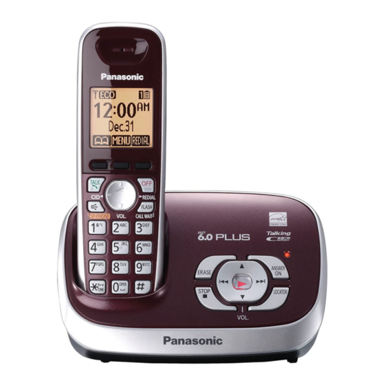
Telephone Equipment
KX-TG6572C
Model No.
KX-TG6572R
KX-TGA653C
KX-TGA653R
Expandable Digital Cordless Answering
System
C: Dark Blue Metallic Version
R: Wine Red Version
(for U.S.A)
© Panasonic System Networks Co., Ltd. 2010
Unauthorized copying and distribution is a violation
of law.
ORDER NO. KM41009258CE
F13
Advertisement
Table of Contents

Related Manuals for Panasonic KX-TG6572C


Summary of Contents for Panasonic KX-TG6572C
- Page 1 Telephone Equipment KX-TG6572C Model No. KX-TG6572R KX-TGA653C KX-TGA653R Expandable Digital Cordless Answering System C: Dark Blue Metallic Version R: Wine Red Version (for U.S.A) © Panasonic System Networks Co., Ltd. 2010 Unauthorized copying and distribution is a violation of law.
- Page 2 KX-TG6572C/KX-TG6572R/KX-TGA653C/KX-TGA653R...
-
Page 3: Table Of Contents
KX-TG6572C/KX-TG6572R/KX-TGA653C/KX-TGA653R TABLE OF CONTENTS PAGE PAGE 1 Safety Precautions----------------------------------------------- 4 16.4. Accessories and Packing Materials ----------------- 83 1.1. For Service Technicians --------------------------------- 4 16.5. Replacement Parts List--------------------------------- 84 2 Warning -------------------------------------------------------------- 4 2.1. Battery Caution--------------------------------------------- 4 2.2. About Lead Free Solder (PbF: Pb free)-------------- 4 2.3. -
Page 4: Safety Precautions
KX-TG6572C/KX-TG6572R/KX-TGA653C/KX-TGA653R 1 Safety Precautions 1.1. For Service Technicians • Repair service shall be provided in accordance with repair technology information such as service manual so as to prevent fires, injury or electric shock, which can be caused by improper repair work. -
Page 5: Discarding Of P. C. Board
KX-TG6572C/KX-TG6572R/KX-TGA653C/KX-TGA653R 2.2.1. Suggested PbF Solder There are several types of PbF solder available commercially. While this product is manufactured using Tin, Silver, and Copper (Sn+Ag+Cu), you can also use Tin and Copper (Sn+Cu), or Tin, Zinc, and Bismuth (Sn+Zn+Bi). Please check the manufacturer's specific instructions for the melting points of their products and any precautions for using their product with other materials. -
Page 6: Specifications
KX-TG6572C/KX-TG6572R/KX-TGA653C/KX-TGA653R 3 Specifications Note: • Design and specifications are subject to change without notice. Note for Service: • Operation range: Up to 300 m outdoors, Up to 50 m indoors, depending on the condition. • Analog telephone connection: Telephone Line... -
Page 7: Technical Descriptions
KX-TG6572C/KX-TG6572R/KX-TGA653C/KX-TGA653R 4 Technical Descriptions 4.1. US-DECT Description The frequency range of 1.92 GHz-1.93 GHz is used. Transmitting and receiving carrier between base unit and handset is same frequency. Refer to Frequency Table (P.59). 4.1.1. TDD Frame Format 4.1.2. TDMA system This system is the cycles of 10 ms, and has 6 duplex paths, but maximum duplex communication path is 5 because of dummy bearer use. - Page 8 KX-TG6572C/KX-TG6572R/KX-TGA653C/KX-TGA653R 4.1.3. Signal Flowchart in the Radio Parts Reception A voice signal from TEL line is encoded to digital data "TXDATA" by BBIC (IC501) in a base unit. Then TXDATA goes to RF PART and it's modulated to 1.9 GHz. The RF signal is amplified and fed to a selected antenna.
-
Page 9: Block Diagram (Base Unit_Main)
KX-TG6572C/KX-TG6572R/KX-TGA653C/KX-TGA653R 4.2. Block Diagram (Base Unit_Main) -
Page 10: Block Diagram (Base Unit_Rf Part)
KX-TG6572C/KX-TG6572R/KX-TGA653C/KX-TGA653R 4.3. Block Diagram (Base Unit_RF Part) ANT2 ANT2 ANT1 DA801 TXON RXON ANT1 KX-TG6572 BLOCK DIAGRAM (Base Unit_RF Part) -
Page 11: Circuit Operation (Base Unit)
KX-TG6572C/KX-TG6572R/KX-TGA653C/KX-TGA653R 4.4. Circuit Operation (Base Unit) General Description: (BBIC, Flash Memory, EERROM) is a digital speech/signal processing system that implements all the functions of speech compression, record and playback, and memory management required in a digital telephone answering machine. The BBIC system is fully controlled by a host processor. The host processor provides activation and control of all that functions as follows. - Page 12 KX-TG6572C/KX-TG6572R/KX-TGA653C/KX-TGA653R 4.4.4. Power Supply Circuit/Reset Circuit The power supply voltage from AC adaptor is converted to VBAT (3.0V) in IC302. And +3.0V for peripherals and analog part is insulated from VBAT by Doubler of BBIC. Circuit Operation:...
- Page 13 KX-TG6572C/KX-TG6572R/KX-TGA653C/KX-TGA653R 4.4.4.1. Charge Circuit The voltage from the AC adaptor is supplied to the charge circuits.
- Page 14 KX-TG6572C/KX-TG6572R/KX-TGA653C/KX-TGA653R 4.4.5. Telephone Line Interface Telephone Line Interface Circuit: Function • Bell signal detection • ON/OFF hook and pulse dial circuit • Side tone circuit Bell signal detection and OFF HOOK circuit: In the idle mode, Q141 is open to cut the DC loop current and decrease the ring load. When ring voltage appears at the Tip (T) and Ring (R) leads (When the telephone rings), the AC ring voltage is transferred as follows: T →...
- Page 15 KX-TG6572C/KX-TG6572R/KX-TGA653C/KX-TGA653R 4.4.6. Parallel Connection Detect Circuit/Auto Disconnect Circuit Function: In order to disable call waiting and stutter tone functions when using telephones connected in parallel, it is necessary to have a circuit that judges whether a telephone connected in parallel is in use or not. This circuit determines whether the telephone connected in parallel is on hook or off hook by detecting changes in the T/R voltage.
- Page 16 KX-TG6572C/KX-TG6572R/KX-TGA653C/KX-TGA653R 4.4.7. Calling Line Identification (Caller ID)/Call Waiting Caller ID Function: Caller ID The caller ID is a chargeable ID which the user of a telephone circuit obtains by entering a contract with the telephone company to utilize a caller ID service. For this reason, the operation of this circuit assumes that a caller ID service contract has been entered for the circuit being used.
- Page 17 KX-TG6572C/KX-TG6572R/KX-TGA653C/KX-TGA653R Call Waiting Caller ID Calling Identity Delivery on Call Waiting (CIDCW) is a CLASS service that allows a customer, while off-hook on an existing call, to receive information about a calling party on a waited call. The transmission of the calling information takes place almost immediately after the customer is alerted to the new call so he/she can use this information to decide whether to take the new call.
-
Page 18: Block Diagram (Handset)
KX-TG6572C/KX-TG6572R/KX-TGA653C/KX-TGA653R 4.5. Block Diagram (Handset) VBAT ANT1 EEPROM 13.824 MHz VBAT CHG_DET RF part CHG_CTL RXON RSTN RESET TXON CHARGE VBAT BATTERY BBIC Receiver HSSPOUTP LOUT 4.0V VBAT CHARGE CP_OFF PUMP (BELL) BELL_LED Monitor SP SPOUTP SPOUTN CKM/STM CKM//STM KEYS... -
Page 19: Block Diagram (Handset_Rf Part)
KX-TG6572C/KX-TG6572R/KX-TGA653C/KX-TGA653R 4.6. Block Diagram (Handset_RF Part) TXON DA801 RXON KX-TGA653 BLOCK DIAGRAM (Handset_RF Part) -
Page 20: Circuit Operation (Handset)
KX-TG6572C/KX-TG6572R/KX-TGA653C/KX-TGA653R 4.7. Circuit Operation (Handset) 4.7.1. Outline Handset consists of the following ICs as shown in Block Diagram (Handset) (P.18). • DECT BBIC (Base Band IC): IC1 - All data signals (forming/analyzing ACK or CMD signal) - All interfaces (ex: Key, Detector Circuit, Charge, EEPROM, LCD) •... - Page 21 KX-TG6572C/KX-TG6572R/KX-TGA653C/KX-TGA653R 4.7.3. Charge Circuit Circuit Operation: When charging the handset on the Base Unit, the charge current is as follows; DC+(6.5 V) → F301 → R371 → R372 →CHARGE+(Base) → CHARGE+(Handset) → Q4 → D7→ F1 → BATTERY+... Battery... BATTERY- → R45 → GND → CHARGE-(Handset)→ CHARGE-(Base) → GND → DC-(GND) In this way, the BBIC on Handset detects the fact that the battery is charged.
-
Page 22: Circuit Operation (Charger Unit)
KX-TG6572C/KX-TG6572R/KX-TGA653C/KX-TGA653R 4.8. Circuit Operation (Charger Unit) Charge control is executed at handset side so that the operation when using charger is also controlled by handset. Refer to Circuit Operation (Handset) (P.20) The route for this is as follows: DC+pin of J1(+) → F1 → R1 → CHARGE+pad → Handset → CHARGE-pad → DC-pin of J1(-). -
Page 23: Signal Route
KX-TG6572C/KX-TG6572R/KX-TGA653C/KX-TGA653R 4.9. Signal Route... - Page 24 KX-TG6572C/KX-TG6572R/KX-TGA653C/KX-TGA653R RF part signal route...
-
Page 25: Location Of Controls And Components
KX-TG6572C/KX-TG6572R/KX-TGA653C/KX-TGA653R 5 Location of Controls and Components Refer to the Operating Instructions. Note: You can download and refer to the Operating Instructions (Instruction book) on TSN Server. 6 Installation Instructions Refer to the Operating Instructions. Note: You can download and refer to the Operating Instructions (Instruction book) on TSN Server. -
Page 26: Test Mode
KX-TG6572C/KX-TG6572R/KX-TGA653C/KX-TGA653R 8 Test Mode 8.1. Engineering Mode 8.1.1. Base Unit... - Page 27 KX-TG6572C/KX-TG6572R/KX-TGA653C/KX-TGA653R Frequently Used Items (Base Unit) ex.) Items Address Default Data New Data Remarks Frequency 00 07 / 00 08 00/01 Use these items in a READ-ONLY mode to confirm the contents. Careless rewriting may 00 02 ~ 00 06 Given value cause serious damage to the computer system.
- Page 28 KX-TG6572C/KX-TG6572R/KX-TGA653C/KX-TGA653R 8.1.2. Handset...
- Page 29 KX-TG6572C/KX-TG6572R/KX-TGA653C/KX-TGA653R Frequently Used Items (Handset) ex.) Items Address Default Data New Data Possible Adjusted Possible Adjusted Remarks Value MAX (hex) Value MIN (hex) Battery Low 00 11 / 00 12 00 / 00 (*2) Frequency 00 07 / 00 08...
-
Page 30: Service Mode
KX-TG6572C/KX-TG6572R/KX-TGA653C/KX-TGA653R 9 Service Mode 9.1. How to Clear User Setting (Handset Only) Handset Press simultaneously until a beep sound is heard. Then single handset is initialized. (The contents of user setting are reset to factory default) *Usage time is not cleared. -
Page 31: Troubleshooting Guide
KX-TG6572C/KX-TG6572R/KX-TGA653C/KX-TGA653R 10 Troubleshooting Guide 10.1. Troubleshooting Flowchart Cross Reference: Check Power (P.32) Check Playback (P.36) Check Record (P.33) Check Battery Charge (P.36) Check Link (P.37) Check the RF part (P.39) Check Handset Transmission (P.44) Check Handset Reception (P.44) Check Caller ID (P.44) - Page 32 KX-TG6572C/KX-TG6572R/KX-TGA653C/KX-TGA653R 10.1.1. Check Power 10.1.1.1. Base Unit Cross Reference: Note: Power Supply Circuit/Reset Circuit (P.12) BBIC is IC501. (*1) Refer to Specifications (P.6) for part number and supply voltage of AC adaptor. (*2) Refer to Circuit Board (Base Unit_Main) (P.73).
- Page 33 KX-TG6572C/KX-TG6572R/KX-TGA653C/KX-TGA653R 10.1.2. Check Record 10.1.2.1. Base Unit Not record Incoming Message Cross Reference: Note: Signal Route (P.23) Flash Memory is IC601. Telephone Line Interface (P.14) BBIC is IC501. Parallel Connection Detect Circuit/Auto Disconnect Circuit (P.15)
- Page 34 KX-TG6572C/KX-TG6572R/KX-TGA653C/KX-TGA653R <How to change the Auto Disconnect activation time and VOX level> A) Auto Disconnect activation time: Some Telephone Company lines (fiber or cable) ON Hook and OFF Hook voltages are lower than conventional lines, which may cause a malfunction of Auto Disconnect detection. To solve this problem, try changing the Auto Disconnect activation through...
- Page 35 KX-TG6572C/KX-TG6572R/KX-TGA653C/KX-TGA653R B) Vox level: It makes easier to detect a small voice (caller) by raising the sensitivity of VOX level. Therefore, the recording of TAM is not turned off during a detection.
- Page 36 KX-TG6572C/KX-TG6572R/KX-TGA653C/KX-TGA653R 10.1.3. Check Playback 10.1.3.1. Base Unit Cross Reference: Note: Power Supply Circuit/Reset Circuit (P.12) Flash Memory is IC601. BBIC is IC1. (*1) Refer to Circuit Board (Base Unit_Main) (P.73). 10.1.4. Check Battery Charge 10.1.4.1. Base Unit Cross Reference: Charge Circuit (P.13) 10.1.4.2.
- Page 37 KX-TG6572C/KX-TG6572R/KX-TGA653C/KX-TGA653R 10.1.5. Check Link 10.1.5.1. Base Unit Cross Reference: Power Supply Circuit/Reset Circuit (P.12) Check the RF part (P.39) Note: *1 How to adjust +3.0V: Execute the command "VDA" Refer to Things to Do after Replacing IC or X'tal (P.57) for Base Unit.
- Page 38 KX-TG6572C/KX-TG6572R/KX-TGA653C/KX-TGA653R 10.1.5.2. Handset Cross Reference: Power Supply Circuit/Reset Circuit (P.20) Check the RF part (P.39) Note: *1 How to adjust +3.0V: Execute the command "VDA" Refer to Things to Do after Replacing IC or X'tal (P.58) for Handset. *2 How to adjust the frequency of X1: To see the frequency, execute the command “SFR“, then check the TP_CKM (IC1-57pin).
- Page 39 KX-TG6572C/KX-TG6572R/KX-TGA653C/KX-TGA653R 10.1.6. Check the RF part 10.1.6.1. Finding out the Defective part After All the Checkings or Repairing 1. Re-register the checked handset to the checked base unit, and Regular HS to Regular BU. Note: (*1) HS: Handset (*2) BU: Base Unit...
- Page 40 KX-TG6572C/KX-TG6572R/KX-TGA653C/KX-TGA653R 10.1.6.2. RF Check Flowchart Each item (1 ~ 6) of RF Check Flowchart corresponds to Check Table for RF part (P.41). Please refer to the each item. Note: (*1) Refer to Check Link (P.37).
- Page 41 KX-TG6572C/KX-TG6572R/KX-TGA653C/KX-TGA653R 10.1.6.3. Check Table for RF part Item BU (Base Unit) Check HS (Handset) Check Link Confirmation Normal 1. Register Regular HS to BU (to be 1. Register HS (to be checked) to Regular checked). HS, BU Mode [Normal Mode] 2.
- Page 42 KX-TG6572C/KX-TG6572R/KX-TGA653C/KX-TGA653R 10.1.6.4. TEST RANGE Check Circuit block which range is defective can be found by the following check. Item BU (Base Unit) Check HS (Handset) Check Range Confirmation TX TEST 1. Register Regular HS to BU (to be checked). 1. Register HS (to be checked) to Regular BU.
- Page 43 KX-TG6572C/KX-TG6572R/KX-TGA653C/KX-TGA653R 10.1.7. Registering a Handset to a Base Unit 10.1.8. Deregistering a Handset 10.1.9. Deregistering All Handsets by the Base Unit...
- Page 44 KX-TG6572C/KX-TG6572R/KX-TGA653C/KX-TGA653R 10.1.10. Check Handset Transmission Cross Reference: Signal Route (P.23) 10.1.11. Check Handset Reception Cross Reference: Signal Route (P.23) Note: When checking the RF part, Refer to Check the RF part (P.39). 10.1.12. Check Caller ID Cross Reference: Telephone Line Interface (P.14) Calling Line Identification (Caller ID)/Call Waiting Caller ID (P.16)
-
Page 45: Disassembly And Assembly Instructions
KX-TG6572C/KX-TG6572R/KX-TGA653C/KX-TGA653R 11 Disassembly and Assembly Instructions 11.1. Disassembly Instructions 11.1.1. Base Unit... - Page 46 KX-TG6572C/KX-TG6572R/KX-TGA653C/KX-TGA653R...
- Page 47 KX-TG6572C/KX-TG6572R/KX-TGA653C/KX-TGA653R 11.1.2. Handset...
- Page 48 KX-TG6572C/KX-TG6572R/KX-TGA653C/KX-TGA653R 11.1.3. Charger Unit...
-
Page 49: How To Replace The Handset Lcd
KX-TG6572C/KX-TG6572R/KX-TGA653C/KX-TGA653R 11.2. How to Replace the Handset LCD Note: The illustrations are simplified in this page. They may differ from the actual product. -
Page 50: Measurements And Adjustments
KX-TG6572C/KX-TG6572R/KX-TGA653C/KX-TGA653R 12 Measurements and Adjustments This chapter explains the measuring equipment, the JIG connection, and the PC setting method necessary for the measurement in Troubleshooting Guide (P.31) 12.1. Equipment Required • Digital multi-meter (DMM): it must be able to measure voltage and current. - Page 51 KX-TG6572C/KX-TG6572R/KX-TGA653C/KX-TGA653R 12.2.2. Connections (Handset) Connect the DC Power or Battery to BATT+ and BATT-. Connect the JIG cable GND (black) to GND. Connect the JIG cable UTX (yellow) to UTX and URX (red) to URX. Note: *: COM port names may vary depending on what your PC calls it.
- Page 52 KX-TG6572C/KX-TG6572R/KX-TGA653C/KX-TGA653R 12.2.3. How to install Batch file into P.C. Note: • “*****” varies depending on the country or models.
- Page 53 KX-TG6572C/KX-TG6572R/KX-TGA653C/KX-TGA653R 12.2.4. Commands (Base Unit) See the table below for frequently used commands. Command name Function Example rdeeprom Read the data of EEPROM Type “rdeeprom 00 00 FF”, and the data from address “00 00” to “FF” is read out.
-
Page 54: Adjustment Standard (Base Unit)
KX-TG6572C/KX-TG6572R/KX-TGA653C/KX-TGA653R 12.3. Adjustment Standard (Base Unit) When connecting the simulator equipment for checking, please refer to below. 12.3.1. Bottom View Note: (*1) is referred to No.2 of Check Check Table for RF part (P.41) (*2) is referred to Power Supply Circuit/Reset Circuit (P.12) -
Page 55: Adjustment Standard (Charger Unit)
KX-TG6572C/KX-TG6572R/KX-TGA653C/KX-TGA653R 12.4. Adjustment Standard (Charger Unit) When connecting the simulator equipment for checking, please refer to below. 12.4.1. Bottom View Digital Volt Meter /2 W DC POWER DC 6.5 V... -
Page 56: Adjustment Standard (Handset)
KX-TG6572C/KX-TG6572R/KX-TGA653C/KX-TGA653R 12.5. Adjustment Standard (Handset) When connecting the simulator equipment for checking, please refer to below. 12.5.1. Component View PNLB1714Z KX-TGA65X ANT_TP RECEIVER C505 C152 C896 C138 R507 C859 C814 C812 C820 C813 C822 C810 R807 C805 C806 C188 R509 CHG_DET 3.0V... -
Page 57: Things To Do After Replacing Ic Or X'tal
KX-TG6572C/KX-TG6572R/KX-TGA653C/KX-TGA653R 12.6. Things to Do after Replacing IC or X'tal If repairing or replacing EEPROM and X'tal, it is necessary to download the required data such as Programming data or adjustment data, etc in memory. The set doesn't operate if it is not executed. - Page 58 KX-TG6572C/KX-TG6572R/KX-TGA653C/KX-TGA653R 12.6.1.2. Handset First, operate the PC setting according to The Setting Method of JIG (P.50). Then download the appropriate data according to the following procedures. Items How to download/Required adjustment EEPROM (IC3) Adjusted parameter data is stored in memory.
-
Page 59: Frequency Table
KX-TG6572C/KX-TG6572R/KX-TGA653C/KX-TGA653R 12.7. Frequency Table Ch. (hex) TX/RX Frequency (MHz) Channel 0 1928.448 Channel 1 1926.720 Channel 2 1924.992 Channel 3 1923.264 Channel 4 1921.536... -
Page 60: Miscellaneous
KX-TG6572C/KX-TG6572R/KX-TGA653C/KX-TGA653R 13 Miscellaneous 13.1. How to Replace the Flat Package IC Even if you do not have the special tools (for example, a spot heater) to remove the Flat IC, with some solder (large amount), a soldering iron and a cutter knife, you can easily remove the ICs that have more than 100 pins. - Page 61 KX-TG6572C/KX-TG6572R/KX-TGA653C/KX-TGA653R 13.1.3. How to Install the IC 1. Temporarily fix the FLAT PACKAGE IC, soldering the two marked pins. *Check the accuracy of the IC setting with the corresponding soldering foil. 2. Apply flux to all pins of the FLAT PACKAGE IC.
-
Page 62: How To Replace The Llp
KX-TG6572C/KX-TG6572R/KX-TGA653C/KX-TGA653R 13.2. How to Replace the LLP (Leadless Leadframe Package) IC Note: This description is only applied on the model with Shield case. 13.2.1. Preparation • PbF (: Pb free) Solder • Soldering Iron Tip Temperature of 700 °F ± 20 °F (370 °C ± 10 °C) Note: We recommend a 30 to 40 Watt soldering iron. - Page 63 KX-TG6572C/KX-TG6572R/KX-TGA653C/KX-TGA653R 13.2.4. How to Install the IC 1. Place the solder a little on the land where the radiation GND pad on IC bottom is to be attached. 2. Place the solder a little on the land where IC pins are to be attached, then place the IC.
-
Page 64: Terminal Guide Of The Ics, Transistors And Diodes
KX-TG6572C/KX-TG6572R/KX-TGA653C/KX-TGA653R 13.3. Terminal Guide of the ICs, Transistors and Diodes 13.3.1. Base Unit 13.3.2. Handset... -
Page 65: Schematic Diagram
KX-TG6572C/KX-TG6572R/KX-TGA653C/KX-TGA653R 14 Schematic Diagram 14.1. For Schematic Diagram 14.1.1. Base Unit (Schematic Diagram (Base Unit_Main)) Notes: 1. DC voltage measurements are taken with voltmeter from the negative voltage line. 2. The schematic diagrams may be modified at any time with the development of new technology. -
Page 66: Schematic Diagram (Base Unit_Main)
KX-TG6572C/KX-TG6572R/KX-TGA653C/KX-TGA653R 14.2. Schematic Diagram (Base Unit_Main) ANT2 R807 C892 RXON ANT2 C822 C827 W 0.2mm W 0.15mm L mm L 20mm 1st layer 3rd layer C894 C826 2.2p W 0.2mm L 10mm C820 1st layer 1.5p ANT1 DA801 C805 C895... - Page 67 KX-TG6572C/KX-TG6572R/KX-TGA653C/KX-TGA653R Q143 +3.0V Q141 REFERENCE R160 1XX : TEL LINE 3XX : POWER, CHARGE 4XX : MIC, SP Q161 5XX : BBIC R141 6XX : FLASH, EEPROM, KEY, LCD 7XX : FOR DK 100k 8XX : RF C165 NC C163 NC...
-
Page 68: Schematic Diagram (Base Unit_Operation)
KX-TG6572C/KX-TG6572R/KX-TGA653C/KX-TGA653R 14.3. Schematic Diagram (Base Unit_Operation) 2APVCC LED902 MEG_LED LED901 ANS_LED KEYS_B KEYIN1 KEYIN2 KEYIN3 KEYS_C KEYS_D KEYS_E ANS1 ERASE MSG2 SKIP MSG1 DOWN LOCAT/INT STOP NC: No Components KX-TG6572 SCHEMATIC DIAGRAM (Base Unit_Operation) - Page 69 KX-TG6572C/KX-TG6572R/KX-TGA653C/KX-TGA653R Memo...
-
Page 70: Schematic Diagram (Handset_Main)
KX-TG6572C/KX-TG6572R/KX-TGA653C/KX-TGA653R 14.4. Schematic Diagram (Handset_Main) Charge Current VBAT VBAT BATT+ 2.5A When on Charge BATT- VBAT 3.0V To Battery CHG_CUR 3.0V C172 CHG(+) 0.1u CHG+ To Charge Terminal E_WP EEP_WP CHG- E_SCL EEP_SCL CHG(-) R43 0 E_SDA EEP_SDA EEP_SCL CHG_CTRL... - Page 71 KX-TG6572C/KX-TG6572R/KX-TGA653C/KX-TGA653R R807 RXON W 0.15mm L 20mm 3rd layer ANT_TP C826 RX_RF W 0.15mm/L 7mm W 0.5mm /L 5mm 1st layer L809 C812 C895 8.2n 1.3p TX_RF DA801 W 0.2mm W 0.15mm L 10.0mm L 20mm 1st layer 3rd layer R806 W 0.15mm...
-
Page 72: Schematic Diagram (Charger Unit)
KX-TG6572C/KX-TG6572R/KX-TGA653C/KX-TGA653R 14.5. Schematic Diagram (Charger Unit) R1 12 SCHEMATIC DIAGRAM (Charger Unit) -
Page 73: Printed Circuit Board
KX-TG6572C/KX-TG6572R/KX-TGA653C/KX-TGA653R 15 Printed Circuit Board 15.1. Circuit Board (Base Unit_Main) 15.1.1. Component View D142 C115 D143 L361 R162 C142 C168 for JIG R122 R167 R165 C126 R163 C167 C184 R181 C186 C512 C475 C473 C513 C472 C120 C123 C124 C525... - Page 74 KX-TG6572C/KX-TG6572R/KX-TGA653C/KX-TGA653R 15.1.2. Bottom View KX-TG6572 CIRCUIT BOARD (Base Unit_Main (Bottom View))
-
Page 75: Circuit Board (Base Unit_Operation)
KX-TG6572C/KX-TG6572R/KX-TGA653C/KX-TGA653R 15.2. Circuit Board (Base Unit_Operation) KX-TG6572 CIRCUIT BOARD (Base Unit_Operation (Component View)) - Page 76 KX-TG6572C/KX-TG6572R/KX-TGA653C/KX-TGA653R Memo...
-
Page 77: Circuit Board (Handset_Main)
KX-TG6572C/KX-TG6572R/KX-TGA653C/KX-TGA653R 15.3. Circuit Board (Handset_Main) 15.3.1. Component View PNLB1714Z KX-TGA65X ANT_TP RECEIVER C505 C152 C896 C138 R507 C859 C814 C812 C820 C813 C822 C810 R807 C805 C806 C188 R509 CHG_DET 3.0V 4.0V CP_CTRL CHG_CTRL Q51 Q52 C127 C110 C172 R562... - Page 78 KX-TG6572C/KX-TG6572R/KX-TGA653C/KX-TGA653R 15.3.2. Bottom View CN3_C SOFT1 MENU SOFT2 TALK LED2 LED5 LEFT RIGHT FLASH DOWN KX-TGA653 CIRCUIT BOARD (Handset_Main (Bottom View))
-
Page 79: Circuit Board (Charger Unit)
KX-TG6572C/KX-TG6572R/KX-TGA653C/KX-TGA653R 15.4. Circuit Board (Charger Unit) 15.4.1. Component View CIRCUIT BOARD (Charger unit (Component View)) 15.4.2. Bottom View TP4 (GND) CIRCUIT BOARD (Charger unit (Bottom View)) -
Page 80: Exploded View And Replacement Parts List
KX-TG6572C/KX-TG6572R/KX-TGA653C/KX-TGA653R 16 Exploded View and Replacement Parts List 16.1. Cabinet and Electrical Parts (Base Unit) PCB2 13(*1) 13(*1) PCB1 Ref.No. Figure Note: (*1) The SPACERs (No.13) are cut from the excess parts of SPACER (No.108) of Cabinet and Electrical Parts (Handset) -
Page 81: Cabinet And Electrical Parts (Handset)
(*1) This cable is fixed by welding. Refer to How to Replace the Handset LCD (P.49). (*2) The rechargeable Ni-MH battery HHR-4DPA is available through sales route of Panasonic. (*3) Attach the SPACER (No. 119) to the exact location described above. -
Page 82: Cabinet And Electrical Parts (Charger Unit)
KX-TG6572C/KX-TG6572R/KX-TGA653C/KX-TGA653R 16.3. Cabinet and Electrical Parts (Charger Unit) 200-1 PCB200 200-2 200-3 200-4 Ref.No. Figure × 8 mm φ... -
Page 83: Accessories And Packing Materials
KX-TG6572C/KX-TG6572R/KX-TGA653C/KX-TGA653R 16.4. Accessories and Packing Materials... -
Page 84: Replacement Parts List
100k L0AA02A00087 SPEAKER R113 ERJ3GEYJ103 PQHG10729Z RUBBER PARTS, SPEAKER R114 ERJ3GEYJ473 PQHR11313Z GUIDE, SPEAKER ABS-HB R121 ERJ3GEYJ394 390k PNKE1055Z1 CASE, CHARGE TERMINAL PS-HB R122 ERJ3GEYJ394 390k (for KX-TG6572C) R131 PQ4R18XJ106 PNKE1055ZA CASE, CHARGE TERMINAL PS-HB R133 ERJ3GEYJ334 330k (for KX-TG6572R) - Page 85 KX-TG6572C/KX-TG6572R/KX-TGA653C/KX-TGA653R Safety Ref. Part No. Part Name & Description Remarks Safety Ref. Part No. Part Name & Description Remarks R141 ERJ3GEYJ104 100k C343 ECUE1H100DCQ 10p R142 PQ4R18XJ272 2.7k C351 ECUV1C104KBV 0.1 R145 ERJ2GEJ222 2.2k C352 ECUV1C105KBV 1 R151 ERJ2GEJ104 100k...
- Page 86 KX-TG6572C/KX-TG6572R/KX-TGA653C/KX-TGA653R 16.5.2. Handset Safety Ref. Part No. Part Name & Description Remarks 16.5.2.1. Cabinet and Electrical Parts UN9219J TRANSISTOR(SI) 2SC6054JSL TRANSISTOR(SI) (DIODES) MA2ZD0200L DIODE(SI) Safety Ref. Part No. Part Name & Description Remarks MA8043M DIODE(SI) MA8043M DIODE(SI) PNGP1085ZA PANEL, (for...
- Page 87 BATCH FILE CD-ROM (*1) 16.5.3. Charger Unit PQZZ430PIR TIP OF SOLDERING IRON (*2) 16.5.3.1. Cabinet and Electrical Parts PQZZ430PRB RUBBER OF SOLDERING IRON (*2) Safety Ref. Part No. Part Name & Description Remarks PNLC1010YC CHARGER UNIT ASS'Y without NAME PLATE (RTL)(for KX-TG6572C)
- Page 88 KX-TG6572C/KX-TG6572R/KX-TGA653C/KX-TGA653R KXTG6572C KXTG6572R KXTGA653C KXTGA653R...