
Related Manuals for Garmin LIDAR-Lite v1 Silver Label


Summary of Contents for Garmin LIDAR-Lite v1 Silver Label
- Page 1 LIDARLite v1 “Silver Label” Operating Manual Updated: 08/13/15 LIDARLite v1 “Silver Label” Manual , Updated: 08/13/15 ...
- Page 2 Table of Contents LIDARLite Specifications Laser Safety Class 1 Laser Product QuickStart Guide Overview Sample Code LIDARLite Signal & Power Interface Definitions J1 Primary interface J2 Secondary signal/power .1” spacing Molex style through hole (Factory Option Only) I2C Protocol Summary Module Mechanical Drawings & Dimensions PCB Dimensions Technology and System Hardware Overview Technology System Hardware LIDARLite Block Diagram Signal Processing Core (SPC) Optical Transmitter and Receiver Background Light Power Conditioning Operational Overview Mode Control Pin Acquisition Settings Internal register space External register space Signal Acquisition Process Correlation Record Processing the Correlative Pulse Processing Velocity Measurement Processing Multiple Reflections Control Register #75(0x4b) (control_reg [75]:) Power Management Control Register #4 (0x04) – Mode Control (control_reg[4]:) Control Register #101 (0x65) (control_reg [101]:) Summary Downloading a Correlation Record Sample C Code Download Correlation Data to a Serial Port Using Put Control Registers ...
- Page 3 Control Register #0 (0x00) (control_reg[0]:) Control Register #1 (0x01) Mode/Status (control_reg[1]:) Control Register #2 (0x02) (control_reg[2]:) Control Register #3(0x03) (control_reg [3]:) Control Register #4 (0x04) – Mode Control (control_reg[4]:) Control Register #5 (0x05) (control_reg[5]:) Control Register #6 (0x06) (control_reg [6]:) Control Register #7 (0x07) (control_reg [7]:) Control Register #8 (0x08) (control_reg [8]:) Control Register #9 (0x09) (control_reg [9]:) Control Register #10(0x0a) (control_reg [10]:) Control Register #11 (0x0b) (control_reg [11]:) Control Register #12 (0x0c) (control_reg [12]:) Control Register #13 (0x0d) (control_reg [13]:) Control Register #14 (0x0e) (control_reg [14]:) Control Register #15(0x0f) (control_reg [15]:) Control Register #16 (0x10) (control_reg [16]:) Control Register #17 (0x11) (control_reg [17]:) Control Register #18 (0x12) (control_reg [18]:) Control Register #19 (0x13) (control_reg [19]:) Control Register #20(0x14) (control_reg [20]:) Control Register #21 (0x15) (control_reg [21]:) Detailed Register Descriptions External Control Register #64 (0x40) Command Control (control_reg[64]:) Control Register #65 (0x41) (control_reg[65]:) Control Register #66 (0x42) (control_reg[66]:) Control Register #67 (0x43) (control_reg[67]:) Control Register #68 (0x44) (control_reg[68]:) Control Register #69 (0x45) (control_reg[69]:) Control Register #70(0x46) (control_reg [70]:) Control Register #71 (0x47) Mode/Status (control_reg[71]:) Control Register #73(0x49) (control_reg [73]:) Control Register #74(0x4a) (control_reg [74]:) Control Register #75(0x4b) (control_reg [75]:) Control Register #76(0x4c) (control_reg [76]:) Control Register #79 (0x4f) (control_reg[79]:) Control Register #81(0x51) (control_reg [81]:) Control Register #82 (0x52) (control_reg [82]:) Control Register #83(0x53) (control_reg [83]:) Control Register #64 (0x40) Command Control (control_reg[64]:) Control Register #65 (0x41) (control_reg[65]:) ...
- Page 4 Control Register #70(0x46) (control_reg [70]:) Control Register #71 (0x47) Mode/Status (control_reg[71]:) Control Register #73(0x49) (control_reg [73]:) Control Register #74(0x4a) (control_reg [74]:) Control Register #75(0x4b) (control_reg [75]:) Control Register #76(0x4c) (control_reg [76]:) Control Register #79 (0x4f) (control_reg[79]:) Control Register #81(0x51) (control_reg [81]:) Control Register #82 (0x52) (control_reg [82]:) Control Register #83(0x53) (control_reg [83]:) Control Register #87 (0x57) (control_reg [87]:) Control Register #88 (0x58) (control_reg [88]:) Control Register #89 (0x59) (control_reg [89]:) Control Register #90 (0x5a) (control_reg [90]:) Control Register #91 (0x5b) (control_reg [91]:) Control Register #92 (0x5c) (control_reg [92]:) Control Register #93 (0x5d) (control_reg [93]:) Control Register #93 (0x5f) (control_reg [95]:) Control Register #96 (0x60) (control_reg [96]:) Control Register #97 (0x61) (control_reg [97]:) Control Register #98 (0x62) (control_reg [98]:) Control Register #99 (0x63) (control_reg [99]:) Control Register #100 (0x64) (control_reg [100]:) Control Register #101 (0x65) (control_reg [101]:) Control Register #104 (0x68) (control_reg [104]:) Control Register #87 (0x57) (control_reg [87]:) Control Register #88 (0x58) (control_reg [88]:) Control Register #89 (0x59) (control_reg [89]:) Control Register #90 (0x5a) (control_reg [90]:) Control Register #91 (0x5b) (control_reg [91]:) Control Register #92 (0x5c) (control_reg [92]:) Control Register #93 (0x5d) (control_reg [93]:) Control Register #93 (0x5f) (control_reg [95]:) Control Register #96 (0x60) (control_reg [96]:) Control Register #97 (0x61) (control_reg [97]:) Control Register #98 (0x62) (control_reg [98]:) Control Register #99 (0x63) (control_reg [99]:) Control Register #100 (0x64) (control_reg [100]:) Control Register #101 (0x65) (control_reg [101]:) Control Register #104 (0x68) (control_reg [104]:) ...
- Page 5 LIDARLite Specifications General Technical Specifications Power 4.755.5V DC Nominal, Maximum 6V DC Weight PCB 4.5 grams, Module 22 grams with optics and housing Size PCB 44.5 X 16.5mm (1.75” by .65”) Housing 20 X 48 X 40mm (.8” X 1.9” X 1.6”) Current Consumption <2mA @ 1Hz (shutdown between measurements), <100mA (continuous operation) Max Operating Temp. 70° C External Trigger 3.3V logic, highlow dge triggered PWM Range Output PWM (Pulse Width Modulation) signal proportional to range, 1msec/meter, 10µsec step size I2C Machine Interface 100Kb – Fixed, 0xC4 slave address. Internal register access & control. Supported I2C Commands Single distance measurement, velocity, signal strength Mode Control Busy status using I2C, External Trigger input / PWM outputs Max Range under typical ~40m conditions Accuracy +/ 2.5cm, or +/ ~1" Default Rep Rate ~50 Hz. LIDARLite v1 “Silver Label” Manual...
-
Page 6: Laser Safety
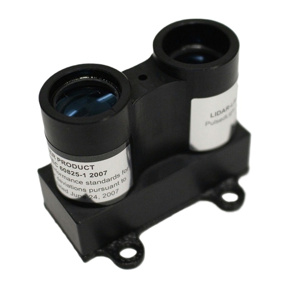
Laser Safety LIDARLite is a laser rangefinder that emits laser radiation. This Laser Product is designated Class 1 during all procedures of operation. This means that the laser is safe to look at with the unaided eye. However, it is very advisable to avoid looking into the beam and power the module off when not in use. No regular maintenance is required for LIDARLite. In the event that the unit becomes damaged or is inoperable, repair or service of LIDARLite is only to be handled by authorized, factorytrained technicians. No service of LIDARLite by the user is allowed. Attempting to repair or service the unit on your own can result in direct exposure to laser radiation and the risk of permanent eye damage. For repair or service please contact PulsedLight directly for a return authorization. No user should modify LIDARLite or operate it without its housing or optics. The operation of LIDARLite without a housing and optics or modification of the housing or optics that exposes the laser source may result in direct exposure to laser radiation and the risk of permanent eye damage. Removal or modification of the diffuser in front of the laser optic may result in the risk of permanent eye damage. Caution – Use of controls or adjustments or performance of procedures other than those specified herein may result in hazardous radiation exposure. PulsedLight is not responsible for injuries caused through the improper use or operation of this product. LIDARLite v1 “Silver Label” Manual , Updated: 08/13/15 ... - Page 7 Class 1 Laser Product This Laser Product is designated Class 1 during all procedures of operation. Parameters Laser Value Wavelength 905nm (nominal) Total Laser Power Peak 1.3Watts Mode of operation Pulsed (max pulse train 256 pulses) Pulse Width 0.5µSec (50% duty Cycle) Pulse Repetition Frequency 1020KHz nominal Energy per Pulse <280nJ Beam Diameter at laser aperture 12mm x 2mm Divergence 4mRadian x 2mRadian (Approx) LIDARLite v1 “Silver Label” Manual , Updated: 08/13/15 ...
- Page 8 QuickStart Guide Overview 1. Make Power and I2C Data Connections as per J 1 connector pin out diagram . Pins 2 & 3 are optional connections and not required. 2. Initialization: Apply Power to the Module. The sensor operates at 4.755.5V DC Nominal, Maximum 6V DC 3. Measurement: Write register 0x00 with value 0x04 (This performs a DC stabilization cycle, Signal Acquisition, Data processing). Refer to the section “ I 2C Protocol Summary ” in this manual for more information about I2C Communications 4. Periodically poll the unit and wait until an ACK is received. The unit responds to read or write requests with a NACK when the sensor is busy processing a command or performing a measurement. (Optionally, wait approx. 20 milliseconds after acquisition and then proceed to read high and low bytes) 5. Read: Register 0x0f, returns the upper 8 bits of distance in cm, register 0x10, returns the lower 8 bits of distance in cm. (Optionally a 2Byte read starting at 0x8f can be done) Sample Code Sample code and wiring for LIDARLite using an Arduino and some other popular platforms can be downloaded by visiting h ttps://github.com/PulsedLight3D .
- Page 9 LIDARLite Signal & Power Interface Definitions J1 Primary interface Board Connector: Molex part #5023860670 (DigiKey Part #: ) W M3917CTND Mating Connector: Molex # 5023800600 PLUG HSG 6POS (DigiKey Part #: W M2271ND) Pin Description PIN 1 POWER_IN – 4.755.5V DC Nominal, Maximum 6V DC. Peak current draw from this input (which occurs during acquisition period) is typically < 100 mA over a duration from 4 to 20ms depending on received signal strength. Unless you use p ower management , the unit will draw 80 mA between acquisition times. PIN 2 POWER_EN Active high, enables operation of the 3.3V microcontroller regulator. Low puts board to sleep, draws <40 μA. (Internal 100K pullup) PIN 3 Mode Select – Provides trigger (highlow edge) PWM out (high) LIDARLite v1 “Silver Label” Manual...
- Page 10 PIN 4 I2C Clock (SCL) PIN 5 I2C Data (SDA) PIN 6 Signal/power ground. J2 Secondary signal/power .1” spacing Molex style through hole (Factory Option Only) Pin Description PIN 1 Laser Bypass 520V max (nominally connected to pin 2 through inductor L8 – removed for external power) PIN 2 POWER_IN – 4.755.5V DC Nominal, Maximum 6V DC PIN 3 POWER_EN Active high PIN 4 External reference clock input (Factory Option – Consult Factory) PIN 5 Signal/power ground. PIN 6 Detector bias – up to 25V external bias for PIN, external bias input 200V for APD (consult factory) LIDARLite v1 “Silver Label” Manual , Updated: 08/13/15 ...
- Page 11 I2C Protocol Summary LIDARLite has a 2wire I2Ccompatible serial interface (refer to I2CBus Specification, Version 2.1, January 2000, available from Philips Semiconductor). It can be connected to an I2C bus as a slave device, under the control of an I2C master device. It supports standard 100 kHz data transfer mode. Support is not provided for 10bit addressing. The Sensor module has a 7bit slave address with a default value of 0x62 in hexadecimal notation. The effective 8 bit I2C address is: 0xC4 write, 0xC5 read. The unit will not presently respond to a general call. The I2C serial bus protocol operates as follows: 1. The master initiates data transfer by establishing a start condition, which is when a hightolow transition on the SDA line occurs while SCL is high. The following byte is the address byte, which consists of the 7bit slave address followed by a read/write bit with a zero state indicating a write request. A write operation is used as the initial stage of both read and write transfers. If the slave address corresponds to the module’s address the unit responds by pulling SDA low during the ninth clock pulse (this is termed the acknowledge bit). At this stage, all other devices on the bus remain idle while the selected device waits for data to be written to or read from its shift register. 2. Data is transmitted over the serial bus in sequences of nine clock pulses (eight data bits followed by an acknowledge bit). The transitions on the SDA line must occur during the low period of SCL and remain stable during the high period of SCL. 3. An 8 bit data byte following the address loads the I2C control register with the address of the first control register to be read along with flags indicating if auto increment of the addressed control register is desired with successive reads or writes; and if access to the internal micro or external correlation processor register space is requested. Bit locations 5:0 contain the control register address while bit 7 enables the automatic incrementing of control register with successive data blocks. Bit position 6 selects correlation memory external to the microcontroller if set. (Presently an advanced feature) 4. If a read operation is requested, a stop bit is issued by the master at the completion of the first data frame followed by the initiation of a new start condition, slave address with the read bit set (one state). The new address byte is followed by the reading of one or more data bytes succession. After the slave has acknowledged receipt of a valid address, data read operations proceed by the master releasing the I2C data line SDA with continuing clocking of SCL. At the completion of the receipt of a data byte, the master must strobe the acknowledge bit before continuing the read cycle. 5. For a write operation to proceed, Step 3 is followed by one or more 8 bit data blocks with acknowledges provided by the slave at the completion of each successful transfer. At the ...
- Page 12 Module Mechanical Drawings & Dimensions Download Housing and Cover in PNG, STL, STEP and SLDPRT formats on GitHub Notes: The hole diameters at their smallest are 0.15" or 0.385 cm with a little rounding erring small LIDARLite v1 “Silver Label” Manual , Updated: 08/13/15 ...
-
Page 13: Pcb Dimensions
PCB Dimensions LIDARLite v1 “Silver Label” Manual , Updated: 08/13/15 ... - Page 14 Technology and System Hardware Overview Technology PulsedLight’s “Timeofflight “distance measurement technology is based on the precise measurement of the time delay between the transmission of an optical signal and its reception. Our patented, high accuracy measurement technique enables distance measurement resolution down to 1cm by the digitization and averaging of two signals; a reference signal fed from the transmitter prior to the distance measurement and a received signal reflected from the target. The time delay between these two stored signals is estimated through a signal processing approach known as correlation, which effectively provides a signature match between these two closely related signals. Our correlation algorithm accurately calculates the time delay, which is translated into distance based on the known speedoflight. A benefit of PulsedLight’s approach is the efficient averaging of lowlevel signals enabling the use of relatively low power optical sources, such as LEDs or VCSEL (VerticalCavity SurfaceEmitting) lasers, for shorterrange applications and increased range capability when using high power optical sources such as pulsed laser diodes. System Hardware The Single Board Sensor provides distance and velocity measurements in an ultrasmall form factor. This small size is the result of PulsedLight's SystemOnChip (SoC) signal processing technology which, beyond being small, reduces the complexity and power consumption of supporting circuitry. The system consists of three key functionalities: ● A Signal Processing Core (SPC) SystemonChip solution encapsulating all the required functions in support of our proprietary range finding system architecture. ● An optical transmitter and receiver tied to the SPC emit and receive a proprietary optical signal pattern generated by the SPC. ● Power Conditioning and I2C signal filtering and buffering. Please refer to “LIDARLite Block Diagram” for a full overview of the system architecture. LIDARLite v1 “Silver Label” Manual , Updated: 08/13/15 ...
- Page 15 LIDARLite Block Diagram Signal Processing Core (SPC) The key component within the system is our SPC chip which implements PulsedLight's signal processing algorithms and primary system architecture. The SPC contains four major subsystems; LIDARLite v1 “Silver Label” Manual , Updated: 08/13/15 ...
- Page 16 1. An 8bit microcontroller provides system control and communications. It contains an I2C slave peripheral. 2. A 500 MHz sampling clock and an associated sampler capture the logic state of the external comparator and convert the data into a slower speed 125 MHz four bit word which is sent to a correlation processor. 3. A correlation processor stores the incoming signal and performs a correlation operation against a stored signal reference with optical burst reception and stores the result in the correlation memory with data points every 2 ns. 4. A transmit signal generator produces an encoded signal waveform with an overall duration of 500 ns that consists of a varying interval pattern of ones and zeroes. These outgoing signal pulses occur at a 20 KHz repetition rate and become either the reference signal or outgoing signal pulse depending on the state of the transmitter. Optical Transmitter and Receiver The optical transmitter and receiver have been designed around the requirements of our signalprocessing algorithm. The transmitter produces optical pulse bursts using signal patterns generated by the SPC. When an optical reference signal is desired, a separate reference transmitter is enabled and driven with the signal pattern using a reference fed to the optical receiver. The reference transmitter has been designed to match the delay and signal shape produced by the higher power signal transmitter. The signal transmitter can drive a variety of optical sources ranging from high speed LEDs, higher power VCSEL laser or much higher power pulsed laser diodes. For the LIDARLite module, the signal transmit driver drives a T13/4 plastic packaged laser diode with a threeamp peak, 50% average duty cycle modulation over a burst duration of 500 ns. The driver has a capability to drive sources at up to 6 A using an external DC power supply. Parameter Transmitter specification Bandwidth 50 MHz, onoff modulation, arbitrary pattern Burst Time/rate 500 ns/20KHz Typology High side current source (programmable), lowside differential current steering Reference Channel 1 A peak (nominal setting) Signal Channel 3 A peak (nominal setting) ...
-
Page 17: Background Light
comparator, specialized analog filtering shapes the return signal originating from the output of the preamplifier. Parameter Receiver specification Bandwidth 50 MHz Detector PIN diode, 500µm by 500µm , 1.5 pF, 1.8 mm diameter lens Virtual Detector size 1 mm – roughly 2X magnification of the package lens Detector Bias Voltage 8 V DC nominal. External Preamp Noise Floor 1 pA/Hz2 Transimpedance Gain 40 K ohm Noise Equivalent Power 12 nW rms Background Light LIDARLite has been designed to operate effectively under a variety of indoor and bright outdoor solar background lighting conditions. The internal optical absorption filter in combination with the detector spectral response provides a transmission band from 800 nm to 1000 nm. Outdoors, this Spectral window allows roughly 14% of the total solar Irradiance to pass to the detector. Assuming a solar constant of roughly 1 KW per meter², and a full receiver field of view of two degrees, we get the following calculated DC solar current and detector shot noise: Bright solar optical background = 6 µW Solar DC current = (6e6 W)(.6 A/W) = 3.6e6 A Shot noise = ((3.6e6 A)(2)(1.6e19)(1/Hz))1/2 = 1 pA/Hz1/2 ... -
Page 18: Power Conditioning
Power Conditioning Multiple voltage references are required by various functions on the LIDARLite board. The standard PIN detector requires a DC bias voltage of roughly 8 V generated by an internal voltage multiplier. The use of optional APD detector requires a temperature dependent bias from 100 V up to 240 V depending on the selected detector. This voltage bias is varied based on the temperature compensation coefficient and is applied through the external detector bias input pin. A factory modification is required to allow external application of detector voltages above 30 V DC. A 3.7 V power supply is used by the receiver circuitry and is enabled by the SPC. Transmitter circuitry typically uses the 5 V nominal supply voltage. By default the power supply pin is coupled to the 5 V input through an isolation inductor. An enable pin allows the internal 3.3 V regulator to be disabled allowing very low power consumption under shutdown conditions. LIDARLite v1 “Silver Label” Manual , Updated: 08/13/15 ... -
Page 19: Operational Overview
Operational Overview Operation of LIDARLite can be separated into two phases; initialization and triggered acquisitions as initiated by the user. During initialization the microcontroller goes through a selftest sequence followed by initialization of the internal control registers with default values. Internal control registers can be customized by the user through the I2C interface after initialization. After the internal control registers are initialized the processor goes into sleep state reducing overall power consumption to under 10 mA. Initiation of a user command, through external trigger or I2C command, awakes a processor allowing subsequent operation. The input of a command through the I2C interfaces may initiate an acquisition or an operation to monitor or modify system parameters. In the event of an acquisition request, the system must first power up and initialize the external functions such as the SPC and transmit/receive circuitry. Acquisition begins with the transmission of a reference burst followed by a signal burst. These signal bursts occur over intervals of roughly 50 100µs depending on the length of the selected correlation record. These signal bursts are repeated until the maximum number of acquisitions have been reached, as defined in the default or user settings or a sufficient number of acquisitions have been performed to achieve a maximum signal strength level. At the completion of the required number of acquisition cycles, the correlation results are processed to calculate the effective time delay of the reference and return within the correlation records. The total acquisition time for the reference and signal acquisitions is typically between 5 and 20ms depending on the desired number of integrated pulses and the length of the correlation record. The acquisition time plus the required 1 msec to download measurement parameters establish a roughly 100Hz maximum measurement rate. Mode Control Pin A bidirectional control and status pin provides a means to trigger acquisitions and return the measured distance via Pulse Width Modulation [PWM] without having to use the I2C interface. The pin driver in the processor has an internal current source pullup of roughly 50uA with the driver output coupled to the user pin through a protection diode allowing only sourcing current into the pin. A lowgoing transition on the mode control pin will trigger a single measurement, and the pin will be actively pulled high with a pulse width proportional to distance. A 1K to 10K ohm termination resistance will solidly pull the pin low to trigger an acquisition state while allowing the pin to still be pulled high during the PWM output pulse. The pulse width follows a 10usec/cm relationship to the measured distance or 1msec per meter. A simple triggering method using a standard microcontroller interface uses a 1K ohm resistor in series with an output pin to pull the mode pin low initiating a measurement with a second port pin used to monitor the lowtohigh output pulse width. If the pin is held low, the acquisition process will repeat indefinitely producing a variable frequency output proportional to distance. ... -
Page 20: Acquisition Settings
Acquisition Settings Signal acquisition parameters can be easily changed to tradeoff system performance parameters. If a high measurement rate is required, then the maximum signal integration time can be reduced to decrease measurement times at the expense of somewhat reduced sensitivity and maximum range. Optical transmit power can be increased by the setting loaded into the Laser Power Register. High pulse power may need to be compensated with an increased spacing between pulse bursts to maintain an acceptable laser duty cycle based on thermal derating requirements. If the length of the correlation record is increased to allow for longer range measurements, increased processing time will decrease the measurement rate. Key control registers impacting acquisitions: Internal register space Register Description control_reg [2] Maximum acquisition count sets the maximum number of acquisition cycles with a maximum value of 255. In most cases an acquisition of 128 is adequate. control_reg [3] Correlation record length establishes the portion of correlation memory allocated to the return signal. The value is broken in to upper and lower LIDARLite v1 “Silver Label” Manual , Updated: 08/13/15 ... - Page 21 nibbles where the lower indicates the starting location and the upper nibble the end point. The nibble value multiplied by 64 is its location in memory. A value of 0xf indicates the end of the record with a value of 1024. control_reg [4] Acquisition mode control establish the enabled acquisition functions such as velocity measurement, lower power consumption states and inhibiting the reference. External register space Register Desciption control_reg [0x43] Laser power control. control_reg [0x4b] Range Processing Criteria for two echoes. Max signal, Max/Min Range. control_reg [0x65] Power management – Sleep states. Signal Acquisition Process After loading new acquisition parameters or retaining default values, a command is sent to the SPC to initiate a signal acquisition. The steps of the acquisition are as follows: 1. Power is applied to the receiver preamp and, after a prescribed delay, the DC offset at the threshold detector is adjusted to set the effective slicing level or threshold in the middle of the noise distribution. The adjustment process is based on the measurement of the one/zero duty cycle at the comparator output. When the signal offset is nulled, the duty cycle of the noise pattern approaches an average of 50%. In more sophisticated applications the threshold can be offset as part of an algorithm to measure the approximate rms value of the noise supporting diagnostics or as part of a voltage control feedback signal supporting an avalanche photo detector biasing. 2. Prior to starting signal acquisition, the correlation memory is cleared and the transmitter is activated to generate a burst signal pattern that is stored in a signature memory that is used as key element in the correlation process. 3. Signal acquisition begins with the activation of the reference portion of the transmitter, followed by the feeding of the signal pattern necessary to generate the optical reference signal which then passes directly to the receiver photo detector. After amplification and zerocrossing detection, this record is stored in the signal memory. ...
- Page 22 6. As in step 4, the stored signal record is correlation processed and then added to any correlation data previously processed and residing in the signal portion of the correlation memory. 7. As the signal and reference acquisitions are repeated, the peak correlation values in the correlation record increase and would ultimately overflow the 12bit word size. To prevent this overflow condition, the correlation process is terminated for either the signal or reference records when a peak signal within the record exceeds a preset maximum value slightly under overflow. Once both the reference and signal records have reached their maximum values or that maximum acquisition count has been exceeded the acquisition process is terminated. 8. After the signal acquisition process is complete, a lowpass and DC restoring filtering process typically cleansup the waveform to improve the final measurement accuracy at low signal conditions and short range. This function can be disabled by resetting the filter enable bit in control register 4 for improved accuracy and resolution at longer ranges. Correlation Record Distance measurements are based on the storage and processing of reference and signal correlation records. The figure below shows a correlation record for a sensor without optics at short distances of 0, 4 and 8 feet. The reference record runs from 063 and the signal record from 64 to 130. Each sample point represents 2nsec or roughly one foot. LIDARLite v1 “Silver Label” Manual , Updated: 08/13/15 ...
- Page 23 The correlation waveform has a bipolar wave shape, transitioning from a positive going portion to a roughly symmetrical negative going pulse. The point where the signal crosses zero represents the effective delay for the reference and return signals. Processing with the SPC determines the interpolated crossing point to a 1cm resolution along with the peak signal value. The figure below illustrates a correlation record example for a longrange system using an avalanche photodiode or APD and laser with a processing chip with a half resolution 2foot/correlation steps and twothousand element signal record. The target is at 660 meters and forms the same bipolar correlation wave shape as in the shortrange system, but in practice the correlation waveform must be distinguished from background noise present in the correlation record. A correlation record detection threshold is established based on the background noise and if no signals are detected above this threshold, a no signal status indication is provided. LIDARLite v1 “Silver Label” Manual , Updated: 08/13/15 ...
- Page 24 The correlation waveform is shown in more detail below. To distinguish the correlation pulse from the background noise, a specialized processing filter follows the envelope of the noise without being significantly affected by signal correlations present in the record. This noise reference is scaled by 1.25 to provide a detection threshold for the correlation. If more than one signal is detected within the correlation record, the return with the next highest signal strength is stored and is available for additional processing. A flag within the status register indicates the LIDARLite v1 “Silver Label” Manual , Updated: 08/13/15 ...
- Page 25 presence of a valid second reflection such as from a window or from a shorterrange object illuminated by the beam. The onboard processing of secondary returns is limited to weaker target reflections in the foreground. The correlation record can be downloaded by the user to examine target details in post processing. Processing the Correlative Pulse The calculation of the effective delay is based on the coarse location within the correlation record and the interpolated crossing between sample points. For the full resolution correlation record used in the LIDARLite processor, each sample represents 2nsec in time or roughly one foot or .3 meters. To obtain a result in cm requires 30 resolution points obtained by interpolating between data points. The figure below illustrates a single correlation pulse obtained by processing either the reference or signal. The correlation waveform on the left shows a zero crossing on the falling edge around the location 185. The detail of the crossing on the right shows a linear fit from the upper crossing point at 185 with a value of 26 and a value at 186 of 44. The calculation of the crossing is equal to (26/ (26 44))*30 or 11.14cm. To get the total delay we multiply the index of the upper point 185 and multiply by 30 to get the coarse delay in cm. The total delay is then 30 * 185 + 10 = 5560. If we have a delay for the reference waveform, with a crossing at 30*30 +15 or 915cm we get a measured delay of 5560915 = 46.45 meters. Processing A module within the processor analyzes the correlation record looking for the largest peak waveform within the record. As it moves through the record, the crossing characteristics of each new larger peak is sampled. At each peak, the coarse delay to the positive sample prior to the zero crossing along with correlation values above and below the crossing and the peak value are stored. With each new peak sample, the previous LIDARLite v1 “Silver Label” Manual , Updated: 08/13/15 ...
- Page 26 peak and the crossing data (now the next largest peak sample) is stored to allow post processing of the data to extract the distance and peak value. The secondary peak in some cases may be the small reflection of the beam passing through a window or possibly the reflection off objects in the foreground. The figure below details the processing flow within the correlation processor after a final correlation waveform is complete. The processed correlation waveform is processed and the various extracted parameters are stored in the external register space. For both the reference and signal records, the coarse record delay and the positive and negative correlation samples are processed to determine the delay in the record to the correlative peak. The difference between the delay measured for the signal and reference determine the effective round trip delay to the target. The delay is scaled to produce a result in centimeters. Signal strength is determined by multiplying the peak value of the correlation by the scaled inverse of the number of acquisitions. It is an inverse relationship because more samples are required to increase the strength of a small signal than a larger one. A valid signal is determined by comparing the signal peak value with the value of the noise floor observed in the range record. LIDARLite v1 “Silver Label” Manual , Updated: 08/13/15 ...
-
Page 27: Velocity Measurement
Velocity Measurement A velocity is measured by observing the change in distance over a fixed time period. The default time period is 100 ms resulting in a velocity calibration of .1 m/s. Velocity mode is selected by setting the most significant bit of internal register 4 to one. When a distance measurement is initiated by writing a 3 or 4 (no dc compensation/or update compensation respectively) to command register 0, two successive distance measurements result with a time delay defined by the value loaded into register at address 0x68. Register (0x68) Load Measurement Period (ms) Velocity Scaling (meters/sec) Value 100 .1 m/s 0xC8 40 .25 m/s 0x50 20 .5 m/s 0x28 10 1 m/s 0x14 Velocity is output as an 8bit Two's Complement signed value read out from register [0x09]. Velocity is the difference between the last two 16bit distance measurements. The previous distance measurement used in the velocity calculation is available from registers [0x14] and [0x15] with [14] containing the most significant byte and [15] the least. To measure velocity with measurement period less than 20 ms, adjustment of the acquisition parameters will likely be necessary. The nominal acquisition is between 1015 ms allowing insufficient time to complete the first velocity acquisition period before starting the second. Measurement acquisition times can be reduced by the elimination of the reference pulse acquisition and performing the acquisition without a prior DC compensation step. The setting of bit position 6 (adjacent to ... - Page 28 Processing Multiple Reflections It is possible to receive multiple valid return signals from a single measurement if the beam illuminates more than one surface along the beam path. This situation may be encountered when the beam clips or passes through an object in the foreground. Because of the inverse square law behavior of the return signal (double the distance get four times less signal) a very small illuminated area near the sensor may produce a much stronger signal than that from the desired target. Ranging objects through a window can produce a strong shorter range signal masking the longer target or conversely it may be desirable to detect a window in the foreground that may only produce a small reflective signal relative to a larger distant reflection. The sensor has the capability to process two distinct reflections as long as they are separated by more than 3.5 meters and the reflection at the shorter distance does not saturate the correlation record masking the more distant object. The “Secondary return” flag in bit position 4 in the status register [1] indicates that a second pulse has been detected. The figure below shows an example of two reflections in the signal correlation record (record address locations greater than 64) separated by approximately 3.5 meters. The sensor detection criteria may be selected to pick the nearer signal, the more distant signal or the strongest signal strength. In addition, when a second pulse is encountered the other reflection can be read from the system without having to perform a new measurement with different detection criteria. Control register 75, summarized below, sets up the criteria for selection of the desired return when two are present. LIDARLite v1 “Silver Label” Manual , Updated: 08/13/15 ...
- Page 29 Control Register #75(0x4b) (control_reg [75]:) Bit 7 Bit 6 Bit 5 Bit 4 Bit 3 Bit 2 Bit 1 Bit 0 Select Max Range Select Range Criteria Select Second Return Notes Default Value 0x00 control_reg [0x4b]: Range Processing Criteria for two echoes. Max signal, Max/Min Range. Bit 0 Select Controls echo processing selection :”1” switches to alternative return; “0” Selects Second Return data associated with detection criteria Bit 1 Select “1” selects return data based on distance; “0” selects strongest return, Range Criteria regardless of distance Bit 2 Select Max “1” selects the longer distance; “0” selects the shorter distance Range The detection criteria is controlled by bit positions 1 and 2. If “Select Range Criteria” is 0 (zero), the system will always select the strongest signal present. In this case, regardless of the number of returns, the strongest return will be measured. If “Select Range Criteria” is one, then the longer or shorter valid return will be selected without consideration of relative signal strength. “Select Max Range” selects the longer or ...
-
Page 30: Power Management
Power Management Two registers can be used to manage power consumption over the acquisition cycle and during idle time between measurements. Bit positions 03 of the Mode Control Register [4] control the power state automatically entered after the completion of an acquisition while Power Control Register [101] sets the present power saving state without requiring a distance measurement. The table below summarizes the control bits of register 4 associated with power management. Control Register #4 (0x04) – Mode Control (control_reg[4]:) Bit Function Bit 7 Velocity Bit 6 Inhibit Reference Bit 5 Velocity Scale factor Bit 4 N/A Bit 3 DET OFF Bit 2 FPGA SLEEP Bit 1 CLK SHUT Bit 0 Preamp Off Notes: Default Value : 0x00 ● Preamp Off : Shutdown preamp between measurements ● ●... - Page 31 Bit 6 Bit 5 Bit 4 Bit 3 Det Bias Disable Bit 2 SLEEP Bit 1 RCVR PWR Disable Bit 0 OSC Disable Notes: ● Default Value : 0x00 ● control_reg [65]: Power control (write only) ● OSC Disable : Disables oscillator reference – Not used in LIDARLite SPC RCVR PWR Disable : Turns on receiver regulator – decreases power consumption by 30 mA when ● inhibited SLEEP : Processor sleep – Reduces power to 20 mA with other hardware disabled ● (wakes on I2C transaction) Send dummy prior to any command or register access operation. ● Det Bias Disable...
- Page 32 Preamp off 30 mA 2 ms Clock Disable 10 mA 1 ms FPGA Sleep 40 mA 10 ms Det. Off 1 mA 1 ms Summary Preamp off : Shutting down the preamp disables the 3.7 V regulator supporting the preamplifier circuitry. The power is stable in 1 2 ms after reenabling after shutdown. The advantage for powering down the preamp between measurements is reduced power consumption and less thermal rise above ambient temperature when operating at low pulse rates 110 Hz. Clock Disable : Is not used in the LIDARLite product. On high performance long range products a crystal oscillator reference is included on the circuit board FPGA Sleep : Disables the phase lock loop (PLL) based internal clock, resulting in the shutdown of all the internal circuitry, except for I2C interface. The I2C interface still monitors buss activity and when its address is detected it initiates the activation of the internal clock. The wakeup time is necessary for the PLL to relock on its internal frequency reference. Detector Off : Shuts off the onboard chargepump generating the 8 V bias to the photodiode. Disabling the chargepump has negligible impact on power consumption, however it eliminates the last of the periodic potential noise sources on the board. ...
- Page 33 Downloading a Correlation Record The following details simplified Ccode routine to download three types of records stored in the system memory. The first selection is a memory bank where the last correlation template pattern is stored. The last received signal record stored is in bank 2 while bank 3 stores the full correlation record. See detailed descriptions of the accessed control registers in Appendix A for a detailed explanation of their function. Note: Only external registers are accessed using this command and the correlation processor cannot be in a sleep state. Sample C Code Download Correlation Data to a Serial Port Using Put This pseudo code can be used as a basis for the download of correlation data for analysis. bank_num – memory banks in the correlation processor 1: template memory 2: last signal record 3: correlation record Function write_twi (register address (hex), value); Function read_twi (register address (hex), number of bytes) Elements – number of words to be transferred read_val is 16 bit integer if (bank_num == 3){ write_twi (0x51, 0x10); // points to the base of the correlation record address write_twi (0x53, (char) (bank_num <<6)); // selects memory bank write_twi (0x40, 0x06); //sets test mode select For (i=0; i<elements; i++) { read_val = (unsigned char) read_twi (0x52, 1); // added to select single byte if (read_twi (0x5d, 1)) read_val |= 0xff00; // if upper byte lsb is set, the value is negative put_dec (read_val); T0_Wait_ms (1); //hold longer than the transfer time for the serial transfer. } write_twi (0x40, 0x00); // return to normal control – null command to control register } ...
-
Page 34: Control Registers
Control Registers Overview The rangefinder can be configured using an I2C machine interface. Settings control the acquisition and processing of ranging data. The I2C interface supports a transfer rate up to 100kb per second. Control Registers are divided between “internal” microprocessor registers and “external” registers residing in the Correlation processor. The internal registers are mapped to register addresses from 0 to 15 hex and external registers from 40 to 68 hex. Internal registers are both read and write, while external registers are read or write only. The most significant bit o f the address byte in the I2C address byte triggers the auto incrementing of register address with successive reads or writes within an I2C block transfer. µP internal Control Registers Register Description control_reg [0x0] Command Control control_reg [0x1] Status system status. control_reg [0x2] Maximum acquisition count control_reg [0x3] Correlation record length setting control_reg [0x4] Acquisition mode control control_reg [0x5] Measured threshold offset during acquisition control_reg [0x67] Measured delay of reference in correlation record control_reg [0x8] Reference correlation measured peak value control_reg [0x9] Velocity Measurement Output control_reg [0xab] Measured delay of signal return in correlation record control_reg [0xc] ... - Page 35 Correlation Core External Control Registers Register Description control_reg [0x40] Command register control_reg [0x41] Hardware Version control_reg [0x42] Preamp DC control control_reg [0x43] Transmit power control control_reg [0x44] Processing range gate (low byte) control_reg [0x45] Processing range gate (high byte) control_reg [0x46] Range Measurement PWM output pin bit[0] used control_reg [0x47] Acquisition status control_reg [0x49] Measured preamp DC offset control_reg [0x4a] Output port control_reg [0x4b] Range Processing Criteria for two echoes. Max signal, Max/Min Range. control_reg [0x4c] 2nd largest detected peak in signal correlation record. control_reg [0x4f] Software Version. control_reg [0x51] Correlation record size select (reference and signal return) control_reg [0x52] Correlation Data access port (low byte) control_reg [0x53] Acquisition Settings selects ext. memory access, signal record select control_reg [0x578] Measured delay of reference or signal in correlation window control_reg [0x59] Correlation peak value of reference or signal control_reg [0x5a] ...
- Page 36 control_reg [0x64] Negative correlation sample after zero crossing (correlation pulse falling edge) control_reg [0x65] Power control settings control_reg [0x68] Velocity measurement window setting register LIDARLite v1 “Silver Label” Manual , Updated: 08/13/15 ...
- Page 37 Detailed Register Descriptions – Internal Unless otherwise noted, all registers contain one byte and are read and write. Control Register #0 (0x00) (control_reg[0]:) Notes ● Command Register ● Write 0x00 to Register 0x00 : Reset FPGA. Reloads FPGA from internal Flash memory – all registers return to default values ● Write 0x01 to Register 0x00: Correlation processing without new acquisition – used to process delay of second peak after bit 0 in control register 0x4b is set to 1 Write 0x02 to Register 0x00: Process correlation without new acquisition – used to reprocess ● Write 0x03 to Register 0x00: Take acquisition & correlation processing without DC correction ● Write 0x04 to Register 0x00: Take acquisition & correlation processing with DC correction ● Control Register #1 (0x01) Mode/Status (control_reg[1]:) Bit Function Notes Bit 7 Eye Safe This bit will go high if eyesafety protection has been activated Bit 6 External Trigger External measurement performed ...
- Page 38 Notes ● Controls M aximum Aquisition Count ● Default Value: 0x80 Range: 0x000xFF (0255). ● ● Control the FPGA maximum signal integration time. ● Stronger signal results in reduced acquisition count to prevent internal register overflow. ● Sig overflow flag and Ref overflow flag in control register 1 are set when automatic limiting occurs. Control Register #3(0x03) (control_reg [3]:) Bit Function Bits 74 Stop address (default 5 corresponding to 512) Bits 30 Start address (default 1 corresponding to 64) Notes ● control_reg[0x51]: Correlation start and stop locations used for signal acquisition (write only) Start address: Value in the range from 0x000x0f – starting point in correlation record (record ● broken into 64 element segments 1024 total Stop address:...
- Page 39 ● Preamp Off : Shutdown preamp between measurements ● CLK SHUT : External Clock Shutdown – Not used in standard LIDARLite ● FPGA SLEEP : Full FPGA sleep after measurement DET OFF : Turns off detector bias after measurement ● N/A: Not used presently ● Velocity Scale factor: “1” sets the velocity measurement separation to 10msec resulting in a ● velocity calibration in meters/sec. A “0” value results in a measurement separation of 100msec. ● Inhibit Reference : If “1” inhibits the acquisition of reference pulses reducing measurement times and reducing measurement variations at the expense of decreasing accuracy over time. “0” allows normal operation ● Velocity: Enable velocity measurement Control Register #5 (0x05) (control_reg[5]:) Notes ● Nominal 128 ●...
- Page 40 Control Register #9 (0x09) (control_reg [9]:) Notes Velocity [Read Only]: in .1 meters/sec (8 bit signed value) ● ● See Mode Control, Register 0x04 for information on changing the scale factor to 1m/sec Control Register #10(0x0a) (control_reg [10]:) Notes ● High byte of calculated delay of signal correlation [Read Only]: calculated after correlation record processing Control Register #11 (0x0b) (control_reg [11]:) Notes Low byte of calculated delay of signal correlation [Read Only]: calculated after correlation ● record processing Control Register #12 (0x0c) (control_reg [12]:) Notes ● Correlation Peak value of signal correlation [Read Only]: (scaled to 0 – 0xff max peak value) Control Register #13 (0x0d) (control_reg [13]:) Notes Maximum noise within correlation record [Read Only]: scaled by 1.25 (typically between ●...
- Page 41 Control Register #15(0x0f) (control_reg [15]:) Notes High byte of calculated delay of signal [Read Only]: reference – calculated after correlation ● record processing ● If the MSB is 1 then the reading is not considered valid. Control Register #16 (0x10) (control_reg [16]:) Notes Low byte of calculated delay of signal [Read Only]: reference – calculated after correlation ● record processing Control Register #17 (0x11) (control_reg [17]:) Notes ● Register shows the required DC compensation command value to maintain zero crossing offset at preamp – Parameter used as part of health flag criteria Control Register #18 (0x12) (control_reg [18]:) Notes ● Added delay between signal bursts [Write Only]: Used to lower transmission duty cycle and pulse frequency Control Register #19 (0x13) (control_reg [19]:) Notes ● Distance Calibration value:...
- Page 42 Control Register #21 (0x15) (control_reg [21]:) Notes ● Previous low byte of calculated delay of signal [Read Only] : reference LIDARLite v1 “Silver Label” Manual , Updated: 08/13/15 ...
- Page 43 Detailed Register Descriptions External Control Register #64 (0x40) Command Control (control_reg[64]:) Bit Description Bit 7 Perform Delay calculation Processing Bit 6 Perform Correlation process Bit 5 Clear Correlation memory Bit 4 Signal acquisition enable Bit 3 Store template pattern enable Bit 0 ... Bit 2 Starting action address Bits 0 through 2 Definitions Value Description 000 No Operation 001 Start processes at template store 010 Start processes at signal acquisition 011 Start processes at clear correlation memory 100 Start processes at Perform Correlation process 101 Start processes at Delay calculation Processing 110 Perform only memory bank access enable 111 Perform only correlation record filtering ...
- Page 44 Control Register #66 (0x42) (control_reg[66]:) Notes Preamp DC control: Range 0255 ● ● Used in DC compensation servo loop Control Register #67 (0x43) (control_reg[67]:) Bit Description Not Used Bits 47 Bits 03 Signal power level control 0x00xf Notes Transmit power control: L aser drive control bits (7 through 4) ref, bits (3 through 0) signal. ● ● Maximum value set at factory 3amps. The maximum output power of the optical source is set through a factory selected resistor which limits available current to the transmit source. ● When using laser devices, which have a much higher operating current, do not increase the reference control level beyond the factory settings. ● Increasing the reference control level may cause premature failure of the internal reference diode. Control Register #68 (0x44) (control_reg[68]:) Notes ● Processing range gate (low byte): Sets the starting location for range processing in the correlation ...
- Page 45 Bit 7 Eye Safe Indicates that eye safety average power limit has been exceeded and power reduction is in place Bit 6 Signal Signal Invalid – “1” No signal detected, “0’ signal detected Invalid Bit 5 Timestamp Active between velocity measurement pairs Bit 4 Second Indicates a second peak was detected. 2nd peak value compared to noise Peak floor Bit 3 PIN Status Indicates the state of the Mode Select external pin. Debounced, masked from output signals, inverted Bit 2 Sig Overflow Overflow detected in correlation process associated with a signal acquisition Bit 1 Ref Overflow detected in correlation process associated with the reference Overflow acquisition Bit 0 Busy Busy, indicates that the processor is actively performing an acquisition process. Control Register #73(0x49) (control_reg [73]:) Notes ● Measured DC value out of correlation sampler input [Read Only]: Value based on the ratio of 1’s and 0’s ...
- Page 46 Notes ● Output port [Write Only Control Register #75(0x4b) (control_reg [75]:) Bit Function Notes Bit 7 Bit 6 Bit 5 Bit 4 Bit 3 Bit 2 Select Max “1” selects the longer distance; “0” selects the shorter distance Range Bit 1 Select Range “1” selects return data based on distance; “0” selects strongest return, Criteria regardless of distance Bit 0 Select Second Controls echo processing selection :”1” switches to alternative return; “0” Return Selects data associated with detection criteria Notes ...
- Page 47 Bits 03 Start Value in the range from 0x000x0f – starting point in correlation record ( Address record broken into 64 element segments 1024 total Notes ● Correlation start and stop locations [Write Only] Control Register #82 (0x52) (control_reg [82]:) Notes ● Data from memory records [Read Only]: Template memory, Signal memory or Correlation memory (low byte of 9 bit value) Control Register #83(0x53) (control_reg [83]:) Bit Function Notes Bits 67 Memory Bank 0:n/a 1: template memory selected, 2: signal memory selected, 3: correlation memory selected. Bit 5 N/A Bit 4 N/A Bit 3 N/A Bit 2 Signal Stop 0: stops signal acquisition at 63 in signal memory 1: stops at location 256 – 8 single bit samples per location ...
- Page 48 Bits 0 through 2 Definitions Value Description 000 No Operation 001 Start processes at template store 010 Start processes at signal acquisition 011 Start processes at clear correlation memory 100 Start processes at Perform Correlation process 101 Start processes at Delay calculation Processing 110 Perform only memory bank access enable 111 Perform only correlation record filtering Notes Command control register: Writing to this register through the I2C interface immediately initiates ● a command operation. Thus it is important to initiate this command only at the completion of defining other registers. Control Register #65 (0x41) (control_reg[65]:) Notes Hardware Version: r evisions begin with 0x01 ● Control Register #66 (0x42) (control_reg[66]:) Notes ...
- Page 49 ● Maximum value set at factory 3amps. The maximum output power of the optical source is set through a factory selected resistor which limits available current to the transmit source. ● When using laser devices, which have a much higher operating current, do not increase the reference control level beyond the factory settings. ● Increasing the reference control level may cause premature failure of the internal reference diode. Control Register #68 (0x44) (control_reg[68]:) Notes Processing range gate (low byte): Sets the starting location for range processing in the ● correlation Control Register #69 (0x45) (control_reg[69]:) Notes ● Processing range gate (high byte) Control Register #70(0x46) (control_reg [70]:) Notes ● Single bit passed from microcontroller PWM output: High at mode pin returns pulse width proportional distance Control Register #71 (0x47) Mode/Status (control_reg[71]:) Bit Function Notes Bit 7 Eye Safe Indicates that eye safety average power limit has been exceeded and ...
- Page 50 Bit 1 Ref Overflow detected in correlation process associated with the reference Overflow acquisition Bit 0 Busy Busy, indicates that the processor is actively performing an acquisition process. Control Register #73(0x49) (control_reg [73]:) Notes Measured DC value out of correlation sampler input [Read Only]: Value based on the ratio of ● 1’s and 0’s Control Register #74(0x4a) (control_reg [74]:) Bit Function Notes Bit 7 Bit 6 Bit 5 Bit 4 Busy Flag Busy flag outputs on mode select pin with I2C initiated acquisition. High causes pin output to be driven low Bit 3 Detector Select receiver detector 1 or 2 – not used in LIDARLite product sel ...
- Page 51 Bit 3 Bit 2 Select Max “1” selects the longer distance; “0” selects the shorter distance Range Bit 1 Select Range “1” selects return data based on distance; “0” selects strongest return, Criteria regardless of distance Bit 0 Select Second Controls echo processing selection :”1” switches to alternative return; “0” Return Selects data associated with detection criteria Notes Range Processing Criteria for two echoes: Max signal, Max/Min Range. ● Control Register #76(0x4c) (control_reg [76]:) Notes Peak Value of 2nd largest pulse in the signal correlation record [Read Only] ● Control Register #79 (0x4f) (control_reg[79]:) Notes Software Version: Revisions begin with 0x01 ● Control Register #81(0x51) (control_reg [81]:) Bit ...
- Page 52 Control Register #83(0x53) (control_reg [83]:) Bit Function Notes Bits 67 Memory Bank 0:n/a 1: template memory selected, 2: signal memory selected, 3: correlation memory selected. Bit 5 N/A Bit 4 N/A Bit 3 N/A Bit 2 Signal Stop 0: stops signal acquisition at 63 in signal memory 1: stops at location 256 – 8 single bit samples per location Bit 1 Signal Start 0: starts signal acquisition at zero in signal memory 1: starts at location 64 – 8 single bit samples per location Bit 0 Reset xmt Resets rotating transmit pattern to base state pattern Notes Acquisition and control settings [Write Only] ● Control Register #87 (0x57) (control_reg [87]:) Notes High byte of calculated delay of reference or signal return [Read Only]: Calculated after ●...
- Page 53 Control Register #90 (0x5a) (control_reg [90]:) Notes Maximum noise within correlation record [Read Only]: Scaled by 1.25 (typically between 0x10 ● – 0x30) Control Register #91 (0x5b) (control_reg [91]:) Notes ● Calculated signal strength [Read Only]: C alculation based on the number of averaged samples and correlation peak value Control Register #92 (0x5c) (control_reg [92]:) Bit Function Notes Bit 7 Bit 6 Bit 5 Bit 4 Bit 3 Bit 2 ...
- Page 54 Notes Measured transmit power [Read Only]: Using internal power monitor ● Control Register #96 (0x60) (control_reg [96]:) Notes Fine delay [Read Only]: Interpolated fine delay (029) ● Control Register #97 (0x61) (control_reg [97]:) Notes Peak Index high byte [Read Only]: Coarse crossing point in the correlation record prior to zero ● crossing Control Register #98 (0x62) (control_reg [98]:) Notes ● Peak Index low byte [Read Only]: Coarse crossing point in the correlation record prior to zero crossing Control Register #99 (0x63) (control_reg [99]:) Notes ● Positive Crossing Upper correlation pulse data value prior to zero crossing ● Used to interpolate fine delay ...
- Page 55 Bit 4 Bit 3 Det Bias Disable Bit 2 SLEEP Bit 1 RCVR PWR Disable Bit 0 OSC Disable Notes: Power control [Write Only] ● ● Default Value : 0x00 ● OSC Disable : Disables oscillator reference – Not used in LidarLite SPC RCVR PWR Disable : Turns on receiver regulator – decreases power consumption by 30mA when ● inhibited ● SLEEP : Processor sleep – Reduces power to 20mA with other hardware disabled (wakes on I2C transaction) Send dummy prior to any command or register access operation. ● Det Bias Disable : Turns off detector bias charge pump Control Register #104 (0x68) (control_reg [104]:) Bit ...
- Page 56 Control Register #88 (0x58) (control_reg [88]:) Notes Low byte of calculated delay of reference or signal return [Read Only]: Calculated after ● correlation record processing Control Register #89 (0x59) (control_reg [89]:) Notes ● Correlation Peak value reference or return [Read Only]: Scaled to 0 – 0xff max peak value ● Used in both signal strength calculation and stored in the appropriate uP control register Control Register #90 (0x5a) (control_reg [90]:) Notes ● Maximum noise within correlation record [Read Only]: Scaled by 1.25 (typically between 0x10 – 0x30) Control Register #91 (0x5b) (control_reg [91]:) Notes Calculated signal strength [Read Only]: C alculation based on the number of averaged samples ● and correlation peak value Control Register #92 (0x5c) (control_reg [92]:) Bit Function ...
- Page 57 Notes Reset [Write Only]: FPGA Core reset – any write to this register ● ● Soft reset of system always occurs with write to register. Control Register #93 (0x5d) (control_reg [93]:) Notes ● Correlation sign bit [Read Only]: MSB of 9 bit signed result ● Most significant bit of signed correlation value Control Register #93 (0x5f) (control_reg [95]:) Notes ● Measured transmit power [Read Only]: Using internal power monitor Control Register #96 (0x60) (control_reg [96]:) Notes ● Fine delay [Read Only]: Interpolated fine delay (029) Control Register #97 (0x61) (control_reg [97]:) Notes ● Peak Index high byte [Read Only]: Coarse crossing point in the correlation record prior to zero crossing ...
- Page 58 Control Register #100 (0x64) (control_reg [100]:) Notes Negative Crossing: Lower correlation pulse data value after zero crossing ● ● Used to interpolate fine delay Control Register #101 (0x65) (control_reg [101]:) Bit Function Bit 7 Bit 6 Bit 5 Bit 4 Bit 3 Det Bias Disable Bit 2 SLEEP Bit 1 RCVR PWR Disable Bit 0 OSC Disable Notes: Power control [Write Only] ● ● Default Value : 0x00 OSC Disable : Disables oscillator reference – Not used in LidarLite SPC ●...
- Page 59 Notes ● Velocity measurement period setting ● 0xc8: gives 100msec pulse separation for .1m/sec velocity register calibration value 0x14 : gives 10msec pulse separation for 1m/sec velocity register calibration value ● LIDARLite v1 “Silver Label” Manual , Updated: 08/13/15 ...