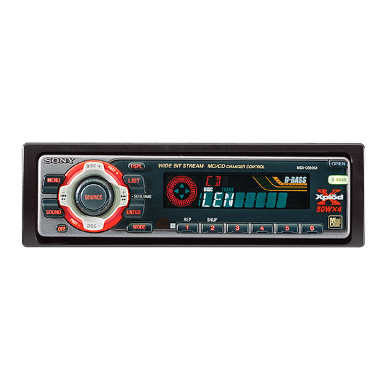
Sony MDX-C6500X Service Manual
Fm/am minidisc player
Hide thumbs
Also See for MDX-C6500X:
- Operating instructions manual (28 pages) ,
- Operating instructions manual (80 pages)
Table of Contents
Advertisement
Quick Links
SERVICE MANUAL
• The tuner and MD sections have no adjustments.
SPECIFICATIONS
AUDIO POWER SPECIFICATIONS (US Model)
POWER OUTPUT AND TOTAL HARMONIC DISTORTION
19 watts per channel minimum continuous average power into
4 ohms, 4 channels driven from 20 Hz to 20 kHz with no more
than 1% total harmonic distortion.
Other Specifications
MD player section
Signal-to-noise ratio
90 dB
Frequency response
10 – 20,000 Hz
Wow and flutter
Below measurable limit
Laser Diode Properties
Material
GaAlAs
Wavelength
780 nm
Emission Duration
Continuous
Laser output power
Less than 44.6 µW*
* This output is the value measured at a distance
of 200 mm from the objective lens surface on the
Optical Pick-up Block.
Tuner section
FM
Tuning range
US, Canadian model:
87.5 – 107.9 MHz
E model:
FM tuning interval:
50 kHz/200 kHz switchable
87.5 – 108 MHz
(at 50 kHz step)
87.5 – 107.9 MHz
(at 200 kHz step)
Antenna terminal
External antenna connector
Intermediate frequency 10.7 MHz/450 kHz
Usable sensitivity
8 dBf
Selectivity
75 dB at 400 kHz
Signal-to-noise ratio
66 dB (stereo),
72 dB (mono)
MICROFILM
MDX-C6500X
Model Name Using Similar Mechanism
Mini Disc Mechanism Type
Optical Pick-up Name
Harmonic distortion at 1 kHz
Separation
Frequency response
AM
Tuning range
Antenna terminal
Intermediate frequency 10.7 MHz/450 kHz
Sensitivity
Dolby noise reduction extension manufactured under license
from Dolby Laboratories Licensing Corporation.
"DOLBY" and the double-D symbol ; are trademarks of Dolby
Laboratories Licensing Corporation.
FM/AM MINIDISC PLAYER
US Model
Canadian Model
E Model
NEW
MG-164NZ-138
KMS-241C/J1NP
0.6% (stereo),
0.3% (mono)
35 dB at 1 kHz
30 – 15,000 Hz
US, Canadian model:
530 – 1,710 kHz
E model:
AM tuning interval:
9 kHz/10 kHz switchable
531 – 1,602 kHz
(at 9 kHz step)
530 – 1,710 kHz
(at 10 kHz step)
External antenna connector
30 µV
– Continued on next page –
1
Advertisement
Table of Contents

Related Manuals for Sony MDX-C6500X


Summary of Contents for Sony MDX-C6500X
- Page 1 MDX-C6500X SERVICE MANUAL US Model Canadian Model E Model • The tuner and MD sections have no adjustments. Model Name Using Similar Mechanism Mini Disc Mechanism Type MG-164NZ-138 SPECIFICATIONS Optical Pick-up Name KMS-241C/J1NP AUDIO POWER SPECIFICATIONS (US Model) POWER OUTPUT AND TOTAL HARMONIC DISTORTION...
- Page 2 DIAGRAMMES SCHÉMATIQUES ET LA LISTE DES PIÈCES SONT CRITIQUES POUR LA SÉCURITÉ DE FONCTIONNEMENT. laser-tap NE REMPLACER CES COMPOSANTS QUE PAR DES PIÈCES SONY DONT LES NUMÉROS SONT DONNÉS DANS CE MANUEL OPTICAL PICK-UP FLEXIBLE BOARD OU DANS LES SUPPLÉMENTS PUBLIÉS PAR SONY.
-
Page 3: Table Of Contents
TABLE OF CONTENTS 1. GENERAL 3. DIAGRAMS Location of Controls ..............4 3-1. IC Pin Descriptions ............19 Getting Started ................. 4 3-2. Block Diagram –MD Section– .......... 27 Setting the Clock ..............4 3-3. Block Diagram –Tuner Section– ........28 MD Player CD/MD Unit (optional) ........ -
Page 4: General
SECTION 1 GENERAL This section is extracted from US, Canadian model’s instruction manual. -
Page 12: Disassembly
SECTION 2 DISASSEMBLY Note : Follow the disassembly procedure in the numerical order given. 2-1. SUB PANEL (MD) ASSY 4 two claws 6 sub panel (MD) assy 2 PTT 2.6x6 3 claw 5 CNP800 1 PTT 2.6x6 2-2. MD MECHANISM BLOCK 6 PTT 2.6x6 7 bracket (MD) 5 MD mechanism block... -
Page 13: Main Board
2-3. MAIN BOARD 4 PTT 2.6x6 6 MAIN board 5 PTT 2.6x6 3 PTT 2.6x8 2 PTT 2.6x8 1 PTT 2.6x8 2-4. HEAT SINK 7 heat sink 6 PTT 2.6x8 5 PTT 2.6x8 4 PTT 2.6x8 3 PTT 2.6x12 2 PTT 2.6x8 1 PTT 2.6x8... -
Page 14: Servo Board
2-5. SERVO BOARD 3 BVTT2x4 4 BVTT2x4 5 SERVO board 1 CN103 2 CN102 2-6. MD COVER ASSY 1 B2 x 3 3 MD cover assy shaft (MD cover guide) cassette holder 2 Pushing the cassette holder in the arrow A direction with a screwdriver, disengage the shaft (MD cover guide) from the groove of MD cover ass’y. -
Page 15: Float Block
2-7. FLOAT BLOCK 4 Pushing the arrow A part, raise the float block upward at the front to unlock. 6 float block 2 spring (float B) float block lever (lock R) lever (lock L) 1 spring (float B) 3 two springs (float F) 2-8. -
Page 16: Lever Assy (Le)
2-9. LEVER ASSY (LE) 2 stopper washer 3 lever ass’y (LE) 4 roller (gear E) 2-10. HOLDER ASSY 0 holder assy 8 stop ring E (1.5) 4 spring (CHKG) 7 stop ring E (1.5) 5 stop ring E (1.5) 6 lever (lock R) 3 lever (lock L) 1 spring (CHKG) 2 stop ring E (1.5) -
Page 17: Chucking Arm Assy
2-11. CHUCKING ARM ASSY 2 chucking arm assy holder assy 2-12. OPTICAL PICK-UP (KMS-241C/J1RP) 4 B2 x 3 6 bearing (SL) 5 feed screw assy 7 optical pick-up (KMS-241C/J1RP) 3 K2 x 3 1 K2 x 3 2 shaft (OPTL) -
Page 18: Motor Assy (Sled) (M902)/Sp Motor Assy (Spindle) (M901)
2-13. SL MOTOR ASSY (SLED) (M902)/SP MOTOR ASSY (SPINDLE) (M901) 4 P1.7 x 1.8 9 P1.7 x 1.8 5 bracket (SL) 2 PSW2 x 8 6 SL motor ass’y (sled) (M902) 0 bracket (SP) 7 B2 x 3 3 SENSOR board qa SP motor assy (spindle) (M901) 8 base (SL) -
Page 19: Diagrams
SECTION 3 DIAGRAMS 3-1. IC PIN DESCRIPTIONS • SERVO BOARD IC301 CXD2652AR (DIGITAL SIGNAL PROCESSOR, DIGITAL SERVO PROCESSOR, EFM/ACIRC ENCODER/DECODER, SHOCK PROOF MEMORY CONTROLLER, ATRAC ENCODER/DECODER, 2M BIT D-RAM) Pin No. Pin Name Pin Description Focus OK signal output to the MD mechanism controller (IC501) MNT0 “H”... - Page 20 Pin No. Pin Name Pin Description Two-way data bus with the D-RAM (IC307) MVCI Digital in PLL oscillation input from the external VCO Not used (fixed at “L”) ASYO Playback EFM full-swing output terminal ASYI I (A) Playback EFM asymmetry comparator voltage input terminal AVDD —...
- Page 21 Pin No. Pin Name Pin Description SRDR Sled servo drive PWM signal (–) output to the BH6511FS (IC303) SFDR Sled servo drive PWM signal (+) output to the BH6511FS (IC303) SPRD Spindle servo drive PWM signal (–) output to the BH6511FS (IC303) SPFD Spindle servo drive PWM signal (+) output to the BH6511FS (IC303) FGIN...
- Page 22 • SERVO BOARD IC302 CXA2523AR (RF AMP, FOCUS/TRACKING ERROR AMP) Pin No. Pin Name Pin Description I-V converted RF signal I input from the optical pick-up block detector I-V converted RF signal J input from the optical pick-up block detector Middle point voltage (+1.65 V) generation output terminal 4 –...
- Page 23 • SERVO BOARD IC501 CXP84340-217Q (MD MECHANISM CONTROLLER) Pin No. Pin Name Pin Description Input of the 4 × 8 matrix test keys (“L” is always output, except in test mode) 1 – 5 TIN3 to TIN7 Not used (open) LOAD Loading motor control signal output to the loading motor drive (IC305) “H”...
- Page 24 Pin Name Pin Description LINKOFF Unilink on/off control signal output for the SONY bus “L”: link on, “H”: link off UNIREQ Data request signal output terminal (for SONY bus) “H”: request on Not used (open) Serial clock signal input from the master controller (IC801) or serial clock signal...
- Page 25 • MAIN BOARD IC801 MN101C49KTB (SYSTEM CONTROL) Pin No. Pin Name Pin Description VREF– — Ground for A/D converter power supply S METER S meter voltage detect signal input FM AGC FM auto gain control signal input KEY IN1 KEY signal input KEY IN0 KEY signal input DSTSEL...
- Page 26 Pin No. Pin Name Pin Description AMP ON Power supply on/off control signal output System attenuate control signal output AMP MUT Power amp attenuate control signal output VOL MUT Mute control signal output for electrical volume TU ON Tuner attenuate signal output EEP SDA Tuner EEPROM serial data signal input/output EEP SCL...
-
Page 27: Block Diagram -Md Section
MDX-C6500X DIGITAL SIGNAL PROCESSOR, 3-2. BLOCK DIAGRAM — MD SECTION — EFM/ACIRC ENCODER/DECODER, SHOCK PROOF MEMORY CONTROLLER, IC301 (1/2) ATRAC ENCODER/DECODER, 2M BIT D-RAM • Signal path IC301 (1/2) EFMO ADDT : MD FILI CLTV SAMPLING FILO RATE CONVERTER IC101... -
Page 28: Block Diagram -Tuner Section
MDX-C6500X 3-3. BLOCK DIAGRAM — TUNER SECTION — PJ400 PJ400 BUS AUDIO IN AUDIO OUT REAR AUDIO OUT FRONT –5 –6 –3 –4 –1 –2 POWER AMP ELECTRONIC VOLUME IC101 IC701 CNP501 AUX L OUT LF FL– TUNER UNIT TU601... -
Page 29: Block Diagram -Display Section
MDX-C6500X 3-4. BLOCK DIAGRAM — DISPLAY SECTION — 3-5. CIRCUIT BOARDS LOCATION SYSTEM CONTROL LCD DRIVE IC801 (2/2) IC901 KEY MATRIX LIQUID CRYSTAL KEY IN0 LCD DATA DATA SENSOR board LSW901-909 DISPLAY PANEL • LCD CE LSW910-915 COM1 LCD901 KEY IN1... - Page 30 MDX-C6500X • Waveforms (MODE:PLAY) THIS NOTE IS COMMON FOR PRINTED WIRING (SERVO BLOCK) BOARDS AND SCHEMATIC DIAGRAMS. (In addition to this, the necessary note is printed in each block.) Approx. for schematic diagram: 0.5Vp-p • All capacitors are in µF unless otherwise noted. pF: µµF 50 WV or less are not indicated except for electrolytics and tantalums.
-
Page 31: Printed Wiring Board -Md Mechanism Section
MDX-C6500X 3-6. PRINTED WIRING BOARD — MD MECHANISM SECTION — (Page 36) • Semiconductor Location Ref. No. Location D401 D501 IC101 IC301 IC302 IC303 IC304 IC305 IC306 (IC307) IC401 IC501 IC502 IC503 Q301 Q302 Q401 (Q402) (Q403) ) : SIDE B... -
Page 32: Schematic Diagram -Md Mechanism Section (1/2)
MDX-C6500X 3-7. SCHEMATIC DIAGRAM — MD MECHANISM SECTION (1/2) — • Refer to page 39 for IC Block Diagrams. Refer to page 28 for waveforms. KMS-241C/JINP Note: • Voltage and waveforms are dc with respect to ground under no-signal conditions. -
Page 33: Schematic Diagram -Md Mechanism Section (2/2)
MDX-C6500X 3-8. SCHEMATIC DIAGRAM — MD MECHANISM SECTION (2/2) — • Refer to page 43 for IC Block Diagrams. Refer to page 30 for waveforms. Note: • Voltage and waveforms are dc with respect to ground under no-signal conditions. no mark : MD PLAY ∗... -
Page 34: Schematic Diagram -Main Section (1/2)
MDX-C6500X 3-9. SCHEMATIC DIAGRAM — MAIN SECTION (1/2) — • Refer to page 42 for IC Block Diagrams. (Page (Page 38) Note: • Voltage and waveforms are dc with respect to ground under no-signal conditions. no mark : MD PLAY ∗... -
Page 35: Schematic Diagram -Main Section (2/2)
MDX-C6500X 3-10. SCHEMATIC DIAGRAM — MAIN SECTION (2/2) — • Refer to page 45 for IC Block Diagrams. Note: • Voltage and waveforms are dc with respect to ground under no-signal conditions. no mark : MD PLAY ∗ : Impossible to measure... -
Page 36: Printed Wiring Board -Main Section
MDX-C6500X 3-11. PRINTED WIRING BOARD — MAIN SECTION — (Page 31) • Semiconductor Location Ref. No. Location Ref. No. Location D401 D924 D402 D925 D404 D926 D405 D927 D601 D928 D603 D930 D-10 D701 E-14 D702 IC101 D801 IC701 D802... -
Page 37: Printed Wiring Board -Relay Section
MDX-C6500X 3-12. PRINTED WIRING BOARD — RELAY SECTION — (Page 36) (Page 40) -
Page 38: Schematic Diagram -Relay Section
MDX-C6500X 3-13. SCHEMATIC DIAGRAM — RELAY SECTION — (Page 34) (Page 39) -
Page 39: Schematic Diagram -Display Section
MDX-C6500X 3-14. SCHEMATIC DIAGRAM — DISPLAY SECTION — (Page 38) Note: • Voltage and waveforms are dc with respect to ground under no-signal conditions. no mark : MD PLAY ∗ : Impossible to measure... -
Page 40: Printed Wiring Board -Display Section
MDX-C6500X 3-15. PRINTED WIRING BOARD — DISPLAY SECTION — • Semiconductor Location Ref. No. Location (D902) B-10 (D903) B-10 (D905) (D951) (Page 37) (IC901) IC951 LED910 B-13 LED911 A-13 LED912 LED913 LED914 B-13 LED915 LED921 LED922 LED923 LED924 ) : SIDE B... -
Page 41: Ic Block Diagrams
3-16. IC BLOCK DIAGRAMS IC301 CXD2652AR 100 99 98 97 96 95 94 93 92 91 90 89 88 87 86 85 84 83 82 81 80 79 78 77 76 75 AUX2 SPINDLE GENERATOR SERVO 74 TE MNT0 73 SE MNT1 MONITOR EACH... - Page 42 IC302 CXA2523AR 43 42 USROP – RF AGC – USRC RFA1 BPF3T RFA2 RFA3 PEAK3T – HLPT –1 – – –2 – OFST PTGR TEMP PEAK – –2 – BOTTOM 36 BOTM – –1 GRVA PBSW 35 ABCD 34 FE –...
- Page 43 IC303 BH6511FS-E2 INTERFACE INTERFACE CHARGE PREDRIVE PREDRIVE PUMP. PREDRIVE PREDRIVE INTERFACE INTERFACE IC305 BA6287F-T1 OUT1 OUT2 DRIVER DRIVER VREF CONTROL LOGIC POWER SAVE IC307 MN41V4400TT-08S TIMING TIMING GENERATOR GENERATOR WRITE COLUMN CLOCK DECODERS SELECTOR GENERATOR INTERNAL REFRESH SENSE ADDRESS CONTROL AMPLIFIERS COUNTER CLOCK...
- Page 44 IC802 BA8270FV-E2 BUS ON BUS ON SWITCH RESET SWITCH BUS ON IN CLK IN BATTERY BATT BATT SWITCH CHECK VREF DATA IN DATA IN/OUT DATA OUT IC901 BA4903ST-V5 5.7V – – REGULATOR VREF THERMAL SHUT DOWN OVER VOLTAGE PROTECT CIRCUIT ON BU+B...
- Page 45 IC701 TDA7402TR 32 31 30 29 28 27 26 25 24 23 MONO SUPPLY FADER MIXER SUBWOOFER MONO MONO +PHASE FADER FADER CONTROL ACINLF OUTPUT CONTROL SWINR SWINL MUTE AC OUTR VOICE AC OUTL BANDPASS C-BUS QUAL. QUAL BASS HIGH OUT DIGITAL TRABLE CONTROL...
-
Page 46: Exploded Views
SECTION 4 EXPLODED VIEWS NOTE: • The mechanical parts with no reference • Color Indication of Appearance Parts The components identified by number in the exploded views are not supplied. mark 0 or dotted line with mark Example : • Items marked “*” are not stocked since 0 are critical for safety. -
Page 47: Front Panel Section
4-2. FRONT PANEL SECTION not supplied (DISPLAY board) LCD901 Ref. No. Part No. Description Remark Ref. No. Part No. Description Remark 3-041-028-01 BUTTON (SOURCE) 3-041-036-01 BUTTON (1-6/M) 3-041-029-01 KNOB (VOL) 3-041-033-01 BUTTON (LIST/ENTER) 3-041-030-01 BUTTON (CROSS) 3-041-035-01 BUTTON (OFF) 3-042-967-01 CUSHION (CROSS) 3-041-034-01 BUTTON (MENU/SOUND) X-3378-396-1 PANEL (S) ASSY, FRONT (US,CND) * 64... -
Page 48: Md Mechanism Section (1)
4-3. MD MECHANISM SECTION (1) (MG-164NZ-138) Ref. No. Part No. Description Remark Ref. No. Part No. Description Remark * 101 A-3326-036-A SERVO BOARD, COMPLETE * 110 3-032-712-01 LEVER (LOCK R) * 102 X-3376-799-1 CHASSIS ASSY, MD 3-919-281-01 SPRING (CHUCKING) 3-032-714-02 SPRING (FLOAT F), TENSION * 112 X-3376-800-1 COVER ASSY, MD 3-921-111-01 SPRING (FLOAT B), TENSION... -
Page 49: Md Mechanism Section (2)
4-4. MD MECHANISM SECTION (2) (MG-164NZ-138) M903 M901 M902 The components identified by Les composants identifiés par une mark 0 or dotted line with mark marque 0 sont critiques pour la 0 are critical for safety. sécurité. Replace only with part number Ne les remplacer que par une piéce specified. -
Page 50: Electrical Parts List
SECTION 5 DISPLAY ELECTRICAL PARTS LIST NOTE: • Due to standardization, replacements in • Items marked “*” are not stocked since The components identified by mark 0 or dotted line with mark the parts list may be different from the they are seldom required for routine service. - Page 51 DISPLAY MAIN Ref. No. Part No. Description Remark Ref. No. Part No. Description Remark R938 1-216-049-11 RES-CHIP 1/10W C202 1-163-009-11 CERAMIC CHIP 0.001uF R939 1-216-049-11 RES-CHIP 1/10W C203 1-163-009-11 CERAMIC CHIP 0.001uF R951 1-216-040-00 RES-CHIP 1/10W C204 1-164-346-11 CERAMIC CHIP R952 1-216-021-00 METAL CHIP 1/10W...
- Page 52 MAIN Ref. No. Part No. Description Remark Ref. No. Part No. Description Remark C811 1-163-259-11 CERAMIC CHIP 220PF D821 8-719-988-61 DIODE 1SS355TE-17 C812 1-163-009-11 CERAMIC CHIP 0.001uF D822 8-719-977-12 DIODE MA8068-M-TX C813 1-164-346-11 CERAMIC CHIP D823 8-719-977-12 DIODE MA8068-M-TX C814 1-163-009-11 CERAMIC CHIP 0.001uF D901...
- Page 53 MAIN Ref. No. Part No. Description Remark Ref. No. Part No. Description Remark JR705 1-216-295-00 SHORT Q906 8-729-049-40 TRANSISTOR STC2412G JR707 1-216-295-00 SHORT Q907 8-729-038-55 TRANSISTOR KRA103S JR709 1-216-295-00 SHORT Q908 8-729-038-68 TRANSISTOR KRC103S JR711 1-216-295-00 SHORT Q911 8-729-038-68 TRANSISTOR KRC103S JR712 1-216-296-00 SHORT Q912...
- Page 54 MAIN RELAY Ref. No. Part No. Description Remark Ref. No. Part No. Description Remark R701 1-216-089-11 RES-CHIP 1/10W R855 1-216-019-00 RES-CHIP 1/10W R703 1-216-206-00 RES-CHIP 2.2K 1/8W R888 1-216-089-11 RES-CHIP 1/10W R704 1-216-295-00 SHORT R901 1-216-246-00 RES-CHIP 100K 1/8W R707 1-216-041-00 METAL CHIP 1/10W R902...
- Page 55 RELAY SENSOR SERVO Ref. No. Part No. Description Remark Ref. No. Part No. Description Remark < DIODE > C324 1-107-826-11 CERAMIC CHIP 0.1uF C325 1-110-563-11 CERAMIC CHIP 0.068uF LED905 8-719-033-14 LED CL-170PG-CD-T (MD WINDOW) C326 1-162-968-11 CERAMIC CHIP 0.0047uF 10% LED906 8-719-033-14 LED CL-170PG-CD-T (MD WINDOW) C327 1-109-982-11 CERAMIC CHIP...
- Page 56 SERVO Ref. No. Part No. Description Remark Ref. No. Part No. Description Remark CN103 1-764-439-21 CONNECTOR, FPC 11P R306 1-216-809-11 METAL CHIP 1/16W R307 1-216-809-11 METAL CHIP 1/16W < DIODE > R308 1-216-809-11 METAL CHIP 1/16W R311 1-216-821-11 METAL CHIP 1/16W D401 8-719-157-93 DIODE DTZ-TT11-3.0B...
- Page 57 SERVO Ref. No. Part No. Description Remark Ref. No. Part No. Description Remark R504 1-216-821-11 METAL CHIP 1/16W MISCELLANEOUS R505 1-216-821-11 METAL CHIP 1/16W *************** R506 1-216-845-11 METAL CHIP 100K 1/16W R507 1-218-708-11 METAL CHIP 4.7K 0.5% 1/16W 1-792-194-21 CORD (WITH CONNECTOR) (POWER) R510 1-216-845-11 METAL CHIP 100K...
- Page 58 MDX-C6500X Ref. No. Part No. Description Remark PARTS FOR INSTALLATION AND CONNECTIONS *************************************** 3-014-370-21 FRAME, FITTING 3-916-012-01 BRACKET (ND), FITTING ASSIST (US,CND) 7-682-160-01 SCREW +P 4X6 (US,CND) X-3368-725-1 SCREW ASSY, FITTING (US,CND) 3-041-027-01 COLLAR X-3366-405-1 SCREW ASSY (EXP), FITTING (E)