Table of Contents
Advertisement
Quick Links
Advertisement
Table of Contents

Related Manuals for Epson M-192G


Summary of Contents for Epson M-192G
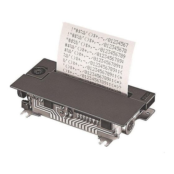
- Page 1 Confidential micro dot printer M-192G Designer’s Guide STANDARD Rev. No. Notes Copied Date Copied by SEIKO EPSON CORPORATION MATSUMOTO MINAMI PLANT 2070 KOTOBUKI KOAKA, MATSUMOTO-SHI, NAGANO, 399-8702 JAPAN PHONE +81-263-86-5353 FAX +81-263-86-9925...
- Page 2 Design Section Sheet Rev. No. Rev. Document Sheet Rev. Sheet Rev. Sheet Rev. Enactment Takeuchi Arai Change Tsukada Hirase Kumagai Change TITLE Front Part M-192G Confidentiality Rev. Table of Agreement Cover Sheet Scope Content Contents Appendix Total Designer’s Guide (STANDARD)
- Page 3 2.4 Paper Exit Design is added, and all the following item numbers are changed. 2.5 Paper Cutter Design: content of 1) is revised, and 4) is added. 2.8 Other Notes on Designing the Outer Case: 4) and 5) are added. TITLE M-192G Designer’s Guide (STANDARD)
- Page 4 2. On the earlier of (a) termination of your relationship with Seiko Epson, or (b) Seiko Epson's request, you must stop using the confidential information. You must then return or destroy the information, as directed by Seiko Epson.
-
Page 5: Table Of Contents
Table of Contents 1 Reference for Circuit Design ........................1 1.1 Waveform Shaping Circuit for Timing Sensor and Reset Detector (Epson Evaluation Circuit) ...1 1.2 Motor Driver Circuit, Print Solenoid Drive Circuit, & Fast Paper Feed Trigger Solenoid Drive Circuit (Epson Evaluation Circuit) .......2 1.3 Major Electronic Components and its Manufacturer..............3... -
Page 6: Reference For Circuit Design
Confidential 1 Reference for Circuit Design 1.1 Waveform Shaping Circuit for Timing Sensor and Reset Detector (Epson Evaluation Circuit) 1SS118 2SA1015 Timing Sensor VCC-O VCC-O DTC143 2.7K – 74HC14 1000pF 0.1uF Reset detector 0.1uF 74HC14 1000pF [User Side] [Printer Side]... -
Page 7: Motor Driver Circuit, Print Solenoid Drive Circuit, & Fast Paper Feed Trigger Solenoid Drive Circuit (Epson Evaluation Circuit)
Confidential 1.2 Motor Driver Circuit, Print Solenoid Drive Circuit, & Fast Paper Feed Trigger Solenoid Drive Circuit (Epson Evaluation Circuit) 2.7K 2SB1261 DTC143 MOTOR ON Motor (+) DTA143 1SS270A nMOTOR 0.1uF 2SD1899 2SA1020 Motor (-) 2.7K DTC143 POWER ON Common for print... -
Page 8: Major Electronic Components And Its Manufacturer
(min) = 100 Ic (max) = −5A 2SB1261 2SD1899 hfe (min) = 100 Ic (max) = 5A STA413A Sanken Zenor-diode contained transistor array Electric 1SS270A Renesas Ic (max) = −2A 2SA1020 Toshiba 1SS118 Renesas SHEET TITLE REVISION EPSON M-192G Designer’s Guide NEXT SHEET (STANDARD) -
Page 9: Outer Case Design Guide
Therefore, the case must be designed so that the manual feed knob does not touch the case when the frame shakes up and down. 7) The case should not touch the printer bottom except near the mounting holes. SHEET TITLE REVISION EPSON M-192G Designer’s Guide NEXT SHEET (STANDARD) - Page 10 Confidential Figure 2.2.1 Figure 2.2.2 SHEET TITLE REVISION EPSON M-192G Designer’s Guide NEXT SHEET (STANDARD)
-
Page 11: Paper Entrance And Paper Holder Design
4) While the printer is in operation, the case may resonate, making the printing noise greater. To prevent this, it is desirable to design the outer case as follows. SHEET TITLE REVISION EPSON M-192G Designer’s Guide NEXT SHEET (STANDARD) - Page 12 5) Attach the ground wire using the printer frame mounting holes (figure 2.2.1; #3 or #4). SHEET TITLE REVISION EPSON M-192G Designer’s Guide NEXT SHEET (STANDARD)