Alinco DJ-G1T Service Manual
Hide thumbs
Also See for DJ-G1T:
- Instruction manual (32 pages) ,
- Manual (3 pages) ,
- Modification (1 page)
Table of Contents
Advertisement
Quick Links
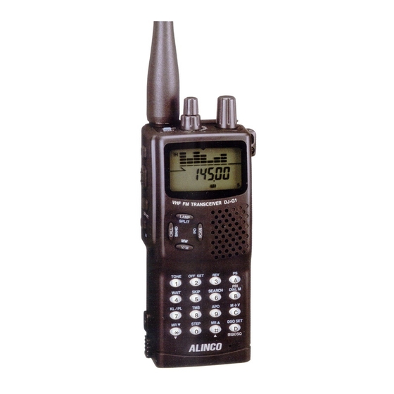
DJ-G1T/E
Service Manual
CONTENTS
•
1) General...................................................................2
2) Transmitter............................................................. 2
3) Receiver..................................................................2
•
1) Receiver System.............................................
2) Transmitter System........................................
3) PLL Circuit...............................................................
4) VCO Circuit.......................................................
5) DTMF Circuit..........................................................
6
) Tone Squelch Circuit.............................................
7) Terminal Function of Microprocessor.........8 - 1 0
8
) Terminal Function of IC302.................................
9) Terminal Function of IC303.................................
•
1) BU4094..................................................................13
2) CM8870CFIT.........................................................14
3) M5218FP............................................................... 15
4) M5237ML.............................................................. 15
5) M67748L............................................................... 16
6
) MB 1505................................................................ 16
7) MX265.................................................................. 17
8
) MJM386................................................................ .18
9) RN5VL45C............................................................ 18
10) X24C08S14-3.0T................................................. 18
11) TK10930VTL......................................................... 19
13).LCD Connection..........................................21 - 2 2
• EXPLODED VIEW
1) Front View 1..........................................................23
2) Front View 2......................................................... 24
3) Rear View ............................................................ 25
4) Charge Unit.......................................................... 26
5) L C D ......................................................................27
E
ALINCO ELECTRONICS INC
•
3
5
_
5 , 6
6
6
- 7
.7
.7
•
11
12
•
...20
•
CIRCUIT DIAGRAM
•
BLOCK DIAGRAM........................................................... 53
RF Unit..........................................................2 8 - 3 0
IF Unit............................................................ 31 - 33
CPU Unit........................................................33 - 34
VCO Unit............................................................... 35
Charge Unit........................................................... 35
Key Unit..................................................................36
PTT Unit................................................................ 36
TSQ Unit................................................................ 36
Mechanical Parts.................................................. 37
Packing.................................................................. 37
1) DJ-G1T Adjustment.............................................38
2) DJ-G1E Adjustment.............................................39
3) Adjustment Points................................................ 40
1) RF Unit Side A......................................................41
2) RF Unit Side B......................................................42
3) IF Unit Side A........................................................43
4) IF Unit Side B........................................................44
5) CPU Unit Side A................................................... 45
6) CPU Unit Side B................................................... 46
7) VCO Unit............................................................... 47
8) KEY Unit................................................................ 48
9) Charge Unit........................................................... 48
10) PTT Unit................................................................ 48
1) RF Unit...................................................................49
2) IF Unit....................................................................50
3) CPU Unit................................................................ 51
4) KEY Unit............................................................... 52
5) Charge Unit......................................................... 52
6) CTCSS Unit.........................................................52
Advertisement
Table of Contents

Related Manuals for Alinco DJ-G1T


Summary of Contents for Alinco DJ-G1T
-
Page 1: Table Of Contents
5) DTMF Circuit............) Tone Squelch Circuit..........• ADJUSTMENT 7) Terminal Function of Microprocessor..8 - 1 0 ) Terminal Function of IC302......... 1) DJ-G1T Adjustment..........38 2) DJ-G1E Adjustment..........39 9) Terminal Function of IC303......... 3) Adjustment Points..........40 • SEMICONDUCTOR DATA 1) BU4094..............13... -
Page 2: Specifications
SPECIFICATIONS 1) General (T version) Frequency Coverage: RX: 108.000- 173.995MHz (T version) RX:440.000 ~ 449.995MHz (T version) TX:144.000 - 147.995MHz RX:144.000 - 145.995MHz (E version) RX:430.000 - 439.995MHz (E version) TX:144.000 - 145.995MHz (E version) Modulation: A3 (receive only) 50£2 Antenna Impedance: Antenna Connector: 7 .2 -12.0V DC max.13.8VDC... -
Page 3: Circuit Description
CIRCUIT DESCRIPTION 1 ) Receiver System The receiver system is the double superheterodyne. The first IF is 30.85MHz and the second IF is 455kHz. 1. Front End 108.00MHz~ 173.995MHz. The receive signal is passed through a low-pass filter (L1, L2, L4, C3, C4, C5 and C7), resonator circuit (L12, varicap D7 and D8), and input to the RF amplifier (Q6). - Page 4 The 455kHz second IF signal is output from Pin3 of IC301, and unwanted frequency band of the second IF signal is eliminated by a ceramic filter (FL301). The resulting signal is led to the Pin5 and 7 of IC301. Demodulator of FM The second IF signal of Pin7 of IC301 is led to the internal limiter amplifier, quadrature detection circuit.
- Page 5 "High" (squelch circuit does not work). This signal "SD" is led to the CPU Pin of IC401, and then processed by CPU. When the squelch circuit is active, Q311 and Q304 are off. When the squelch circuit does not work, Q311 and Q304 are on.
-
Page 6: Pll Circuit
VR308 and the middle power setting variable resistor VR307 located in the IF unit. The radio has no low power setting variable resistor. High Middle Power D306A D306B 3) PLL Circuit The PLL serial data (clock, data, strobe) is sent from CPU IC401. The Pin9 of IC2 is clock, Pin10 of IC2 is data, Pin 11 of IC2 is strobe. -
Page 7: Tone Squelch Circuit
Each of the oscillation frequency of VC01 and VC02 is as follows. Tune Varicap Oscillation Frequency 108.00MHz~ 139.995MHz 138.85MHz~170.845MHz VC01 140.00MHz~173.995MHz 170.85MHz~204.845MHz 134.575MHz~169.57MHz 144.00MHZ-147.995MHz (TTX) (E TX) 144.00MHz-145.995MHz VC02 420.00MHz~429.995MHz 450.85MHz~460.845MHz 430.00MHz~449.995MHz 399.15MHz~419.145MHz 450.00MHz~479.995MHz 419.15MHZ-449.145MHz 800.00MHz~999.99M Hz 384.575MHz~484.57MHz 5) DTMF Circuit 1. -
Page 8: Terminal Function Of Microprocessor
7) Terminal Function of Microprocessor Description Remarks Pin Name Name Signal AD Converter Power Supply Terminal AVcc M RC Microphone Remote Control Input Power Supply Voltage Detection SM T S-Meter Input AVss AD Converter Ground TES T Connect to Vdd OSC1 M CU Internal Clock Input Xout... - Page 9 Remarks Description Pin Name Signal Name DTM F Signal Input DTOE R13/EVNB Sub Tone Signal Output R20/EVND TONEO Sub Tone Signal Output R21/SCK TONE1 TONE2 Sub Tone Signal Output R22/SI Sub Tone Signal Output R23/SO TO N E3 DTM F 4-Bit Data Input R30/SEG1 R31/SEG 2 DTMF 4-Bit Data Input...
- Page 10 Description Remarks Pin Name Signal Name SEG13 LCD SEG13 SEG30 LCD SEG14 SEG31 SEG14 LCD SEG15 SEG32 SEG15 SEG16 LCD SEG16 SEG33 SEG34 SEG17 LCD SEG17 LCD SEG18 SEG35 SEG18 SEG36 SEG19 LCD SEG19 SEG37 SEG20 LCD SEG20 LCD SEG21 SEG38 SEG21 SEG39...
-
Page 11: Terminal Function Of Ic302
8) Terminal Function of IC302 BU4094BF-T1 Remarks Pin Name Signal Name Description STROBE STB3 DATA DATA CLOCK AFPC Power Supply Control for AF Power Amp. Power Supply Control for RX 5V AF Switch AM Switch Os’ IC303 (2) Power Supply Control for TX 5V SUBC Power Supply Control for Sub Band 360C... -
Page 12: Terminal Function Of Ic303
9) Terminal Function of IC303 BU4094BF-T1 Pin Name Signal Name Description Remarks STROBE STB3 DATA DATA IC302 (10) CLOCK MAINC Power Supply Control for Main Band VC02C Power Supply Control (or VHF VCO VC01C Power Supply Control for UHF VCO VHF VCO Shift ON/OFF Power Supply ON/OFF of VCO and PLL TX Middle Power Control... -
Page 13: Semiconductor Data
SEMICONDUCTOR DATA 1) BU4094 (XA0246) 8-Stage Shift Register HZ 1 STROBE z □ Output Enable DATA CLOCK ÜZ Function Table Parallel outputs Serial outputs Output Clock Strobe Data enable No Chg. No Chg. No Chg. N o Chg. No Chg. Q n-l No Chg. -
Page 14: Cm8870Cfit
2) CM8870CFIT (XA0231) CTCSS Encoder/Decoder CJ 1 St/Gt Vref c z = IN H OSC1 OSC2 Decode Ta ble Function Table F high Nam e Description F low 1209 Inverting Input Noninverting Input 1336 Gain Selection 1477 Vref Reference Voltage Output 1209 1336 Power Down Control... -
Page 15: M5218Fp
3) M5218FP (XA0068) Dual Low Noise Operational Amplifiers I e Power Supply Plus Output 1 1 I | 7 Output 2 Inverting Input 1 2 [ | 6 Inverting Input 2 Noninverting Input 1 3 [ I 5 Noninverting Input 2 Power Supply Minus 4 I 4) M5237ML (XA0217) Voltage Regulator... -
Page 16: M67748L
5) M67748L (XA0148) 135~150MHz 7W RF Power Module 6) MB1505 (XA0240) PLL Frequency Synthsizer OSCin O S C o u tIZ Z 2 Z D oP (out □ BiSW 10 Z Z 3 Data 9 = □ Clock Function Table Nam e Function OSCin... -
Page 17: Mx265
7) MX265 (XA0241 ) CTCSS Encoder/Decoder MX265DW 0.1MF H I— XTAL/CLOCK < 5 'p L i Z l -«— II---- XTAL TONE IN O.lnF -----II--- LOAD/LATCH BIAS SERIAL ENABLE R ttTX 0.1MF SERIAL DATA TONE OUT 560K -vw— SERIAL CLOCK RX DETECT DECODE COMP. -
Page 18: Rn5Vl45C
8) NJM386 (XA0061) Gain Gain Power Amplifiers -Input Bypass V+=9V R L = 1 6 fi Po=500mW +tnput CT> Vout 9) RN5VL45C (XA0232) Voltage Detector Equivalent Circuit 10) X24C08S14-3.0T (XA0226) EEPROM 256 x 8Bit Pin Names 14 Z Z NC NC IZ Z Symbol Description... -
Page 19: Tk10930Vtl
11) TK10930VTL (XA0223) Characterristic Symbol Typical Typical Condition Supply Current 1 Icc1 No signal, AM ON Supply Current 2 Icc2 No signal, AM O FF Mixer Conversion Gain Mixer Input Impedance DC Test Limiting Sensitivity Limit -3.0dB Output Voltage mVrms 10mVin +/-3kHz DEV Distortion THD1... -
Page 20: Transistor, Diode And Led Outline Drawings
12) Transistor, Diode and LED Outline Drawings Top View... - Page 21 (SEG20) 48 (COM2) (COM 1) (SEG21) 45 (S EG 19) 44 (SEG18) 43 (S EG 17) 42 (S EG 16) 41 (SEG15) 40 (SEG14) 39 (S EG 13) 38 (S EG 12) 37 (SEG11) 36 (SEG10) 35 (SEG9) (SEGS) (SEG7) (S E G 6) (SEG5) (SEG4)
- Page 22 SEG29) SEG27) SEG25) SEG 23) <D SEG22) 5‘ SEG24) SEG26) COMO) C O M 1) COMO) SEG28) SEG30) SEG 32) SEG34) SEG 35) SEG33) SEG31)
- Page 23 (SEG20) 48 (COM 2) (C 0 M 1 ) (SEG21) 45 (SEG 19) 44 (S E G 18) 43 (SEG17) 42 (SEG16) 41 (SEG 15) 40 (SEG 14) 39 (SEG13) 38 (SEG12) 37 (S E G 11) 36 (SEG 10) 35 (S E G 9) (S E G 8) (SEG 7)
- Page 24 (SEG29) (SEG27) (SEG25) (SEG23) (SEG22) (SEG24) (SEG26) (COMO) (NC) (C O M 1) (NC) (COMO) (SEG28) (NC) (NC) (NC) (NC) (NC) (SEG30) (SEG32) (SEG34) (SEG35) (SEG33) (SEG31)
- Page 25 to ÎO...
- Page 26 (SEG29) (SEG27) (SEG25) (SEG23) (SEG22) (SEG24) (SEG26) (COMO) (NC) (COM 1) (NC) (COMO) (SEG28) (NC) (NC) (NC) (NC) (NC) (SEG30) (SEG32) (SEG34) (SEG35) (SEG33) (SEG31)
-
Page 28: Front View 1
2) Front View 2 f AF0012... -
Page 29: Rear View
3) Rear View IF Unit AK0005 TS0078 Charge Unit FY0001 0 T © AK0005 ! F M 0 0 8 ^ j^ AG0001; AK0005 AZ0012... -
Page 30: Charge Unit
4) Charge Unit AF0025... -
Page 31: Lcd
5) LCD... -
Page 32: Parts List
Parts List R F Unit R e f. R e f. P a r ts N a m e P a r ts N a m e P a r ts N o . D e s c r ip t io n N O . -
Page 33: Rf Unit
RF Unit Ref. Ref. Parts Name Parts No. Description Parts Name Parts No. Description — C 102 C 1608JB 1H 102K T-A Q C 0276 Coil N L252018T-R 10J C 103 C U 3035 Chip C. C 104 Chip C. Q C 0276 Coil N L252018T-R 10J... - Page 34 RF Unit Ref. R e f. Parts Name Parts No. Description P a r ts N o . D e s c r ip t io n P a r ts N a m e N o . C hip R. E R J3G S Y J101V (E) E R J3G S V J103V RK 3026...
-
Page 35: If Unit
IF Unit R e f. R e l. P a r ts N a m e D e s c r ip tio n P a r ts N a m e P a r ts N o . P a r ts N o . D e s c r ip t io n N o . - Page 36 IF Unit Ref. Ref. Parts Name Parts Name Parts No. Description Parts No. Description E R J3G S Y J102V Chip R. R313 RK303S D 305 E R J3G S Y J104V R314 RK 3062 Chip R. D 306 X L0128 Diode M A 713TX Chip R.
- Page 37 IF Unit/CPU Unit R e f. R e f. P a r ts N a m e P a rts N a m e P a r ts N o . D e s c r ip tio n P a r ts N o . D e s c r ip tio n N o .
-
Page 38: Cpu Unit
CPU Unit Ref. Ref. Parts Name Parts No. Description Parts Name Parts No. Description ER J3G S Y J104V DA227TL RK3062 Chip. R R 430 D411 X D 0238 Diode E R J3G S Y J473V Chip. R DA227TL R431 RK3058 D412 X D 0238... -
Page 39: Vco Unit
VCO Unit/CHARGE Unit Ref. Ref. Parts Name Parts Name Parts No. Description Parts No. Description CHARGE Unit VCO Unit C 1608JB 1H102K T-A CU3031 Chip C. C 1608JB 1H471K T-A Chip C. C501 C201 C U 3035 Chip C. C160SJB 1H 471K T-A C 202 C 1608JB 1H 102K T-A C 502... -
Page 40: Key Unit
KEY Unit/PTT Unit/TSQ Unit Ref. Ref. Parts Name Parts Name Parts No. Description Parts No. Description KEY Unit TSQ Unit Chip C. C 16 0 8 C H 1 H 2 2 1JT-A D601 XL0016 SLM -13M W C701 C U 3027 C 1608C H 1H 221JT -A D602 XL0016... -
Page 41: Mechanical Parts
SQ L Knob VO L Knob N K 0033 NK 0034 Dial Knob Rear C ase KB0041A Front C ase DJ-G1T K M 0154 P R 0237 FCC Part 15 Seal S P Holder S T 00 40 T G 0016A... -
Page 42: Adjustment
Adjustment 1) DJ-G1T Adjustment Mesurement point Adjustment Freq. Specification Item TX/RX Point or condition (MHz) 1.0+/-0.1V L202 146.05 1.8+/-0.1V L203 445.05 Reference TX Frequency 146.05 146.05MHz+/-50Hz Frequency 12dB SINAD 146.05 12dB SINAD is MAX Sensitivity below -9dBpV (ENF) 12dB SINAD... -
Page 43: Dj-G1E Adjustment
2) DJ-G1E Adjustment Freq. Mesurement point Adjustment Specification Item TX/RX or condition Point (MHz) 0.9+/-0.1 V 145.05 L202 1.4+/-0.1V 433.05 L203 Reference 145.05 TX Frequency 145.05MHZ+/- 50Hz Frequency 12dB SINAD 145.05 12dB SIN AD is MAX Sensitivity below -9dB|iV (ENF) 12dB SINAD 433.05 Check... -
Page 44: Adjustment Points
3) Adjustment Points IF Unit (• V R 3 0 5 CZZ) I--» V R 3 0 6 V R 3 0 7 = F t V R 3 0 8 = F t V R 3 0 3 RF Unit... -
Page 45: Pc Board View
PC BOARD VIEW 1) RF Unit Side A UP0237 D JG10 R F-IF Flexible PCB •; • ' j k i m ic j a c k ; ; , 102-0 i - 540 >JK2„ ? S P JflC K ' HF>.il-i93-01-di0 : 2P1 (E) ■... - Page 46 4 ^ ro...
-
Page 47: If Unit Side A
3) IF Unit Side A TBS?]: BRPf ¡120.1 W U P 0237 RF-IF Flexible PCB... -
Page 48: If Unit Side B
4) IF Unit Side B... -
Page 49: Cpu Unit Side A
5) CPU Unit Side A C P U -IF Flexible PCB ------------------------------------------------------------------------------------ ------- ----------------- 1 > P T T PCB... -
Page 50: Cpu Unit Side B
6) CPU Unit Side B P T T P C B ^Jj4iK fey” ffle^ible'PCB UP0236 CPU-1F Flex. -
Page 51: Vco Unit
7) VCO Unit Side A 0 2 0 3 . ' . <» > 1 < o RF O lfT : « &2CP. i P-H.-l i SideB... -
Page 52: Key Unit
8) KEY UNIT sari f — i m m m 9) Charge UNIT 10) PTT UNIT S501-S504 UU00Î5 SKOD-901... - Page 53 S ü ÿ î & î ! I » I § I ? S í t i s 9 I < « o a a < « s S m TTTTTm TTTÏÏTÏÏTTT^ UNO dU U l A J V d O V I Q 0 I ± V I / \ I 3 H 0 S...
-
Page 54: If Unit
IF UNIT 8 S B| i * * p s a g g | ' g ! l B, , s s s s s Ly-< H H > -< M H H >-<>-< S o e v » V x - . T w «... -
Page 55: Cpu Unit
3) CPU Unit... -
Page 56: Key Unit
4) KEY UNIT 1 ■ □601 D602 R601 1®° SLM-13MW X 2 D603 D604 „ r t R602 ■vw —W ---- H ---- , 0 0 S L M I 3 M W X 2 5) CHARGE UNIT JK501 H Ë C 27B I-01-020 UJ0015 6) CTCSS Unit EJ-16U... - Page 57 A M P (A M )
- Page 58 PHONE: 069-786018 FAX: 069-789-60766 Italy: ALINCO ELECTRONICS S.R.L. Via Straffora, 35/D, 20090 Opera (Milano), Italy PHONE: 02-57605160 FAX: 02-57606091 China: ALINCO ELECTRONICS (Beijing Office) Beijing Fortune Bldg. Room 918-A No.5 Dong San Huan Bei Lu, Chaoyang District Beijing China PHONE: 01-501-7561 FAX: 01-501-7560...