Table of Contents
Advertisement
Quick Links
SERVICE
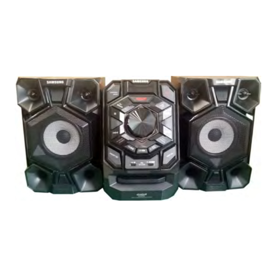
MINI-Compact System
MX-J730
Refer to the service manual in the GSPN (see the rear cover) for more information.
MINI-Compact System
Model Name
Model Code
MANUAL
1. Precaution
2. Product Specification
3. Disassembly and Reassembly
4. Troubleshooting
5. PCB Diagram
6. Schematic Diagram
MX-J730
MX-J730/XA
Contents
Advertisement
Table of Contents

Related Manuals for Samsung MX-J730


Summary of Contents for Samsung MX-J730
- Page 1 MINI-Compact System Model Name MX-J730 Model Code MX-J730/XA SERVICE MANUAL MINI-Compact System Contents 1. Precaution 2. Product Specification 3. Disassembly and Reassembly 4. Troubleshooting 5. PCB Diagram 6. Schematic Diagram MX-J730 Refer to the service manual in the GSPN (see the rear cover) for more information.
-
Page 2: Table Of Contents
SMPS PCB Top........................5 − 9 5.6.1. Pin Connection ......................5 − 10 5.7. SMPS PCB Bottom ........................5 − 11 Schematic Diagram ........................... 6 − 1 6.1. Overall Block Diagram ......................6 − 1 Copyright© 1995-2013 SAMSUNG. All rights reserved. - Page 3 MAIN-2..........................6 − 6 6.7. MAIN-3..........................6 − 7 6.8. MAIN-4..........................6 − 8 6.8.1. Test Point Wave Form ....................6 − 9 6.9. MAIN-5..........................6 − 10 6.10. SMPS ............................ 6 − 11 Copyright© 1995-2013 SAMSUNG. All rights reserved.
-
Page 4: Precaution
ON to the OFF position, measure the current between a known ground and all exposed metal parts. Known Grounds - Earth Known Metal parts - screwheads, metal cabinets, etc. Figure 1.1 AC Leakage Test Copyright© 1995-2013 SAMSUNG. All rights reserved. - Page 5 A replacement part that does not have the same safety characteristics as the original might create shock, fire or other hazards. Copyright© 1995-2013 SAMSUNG. All rights reserved.
-
Page 6: Servicing Precautions
CAUTION First read the “Safety Precautions” section of this manual. If some unforeseen circumstance creates a conflict between the servicing and safety precautions, always follow the safety precautions. Copyright© 1995-2013 SAMSUNG. All rights reserved. -
Page 7: Precautions For Electrostatically Sensitive Devices (Esds)
8) Minimize body motions when handling unpackaged replacement ESDs. Motions such as brushing clothes together, or lifting a foot from a carpeted floor can generate enough static electricity to damage an ESD. Copyright© 1995-2013 SAMSUNG. All rights reserved. -
Page 8: Installation Precautions
5) Installing the product in a special place like below rather than normal environment may cause serious quality concerns due to its special conditions. If this is the case, make sure to contact a local Samsung service center before installing the product. -
Page 9: Product Specification
USB Host (Twin USB) • TV Sound Connect • Bluetooth • BT Power On ■ Disc • Type : 1 Tray (12 cm CD) • Compatible : CD DA / CD-R / RW, WMA, MP3, ISO9660 Copyright© 1995-2013 SAMSUNG. All rights reserved. -
Page 10: Specifications
Input sensitivity (AUX) 2V NOTE • Samsung Electronics Co., Ltd reserves the right to change the specifications without notice. • Weight and dimensions are approximate. • Design and specifications are subject to change without prior notice. • For the power supply and Power Consumption, refer to the label attached to the product. -
Page 11: Specifications Analysis
232 (W) X 331 (H) X 294 (D) 223 (W) X 325 (H) X 280 (D) 230 (W) X 359 (H) X 299.7 (D) SPK SIZE (mm) Package Weight 12.2 11.71 (Kg) O : Feature Included X : Not Included Copyright© 1995-2013 SAMSUNG. All rights reserved. -
Page 12: Accessories
2. Product Specification 2.4. Accessories 2.4.1. Supplied Accessories Accessories Item Item code Batteries (AAA) 4301-000116 Remote Control AH59-02694B User’s Manual AH68-02791D FM Antenna AH42-00021A Copyright© 1995-2013 SAMSUNG. All rights reserved. -
Page 13: Disassembly And Reassembly
In order to assemble reverse the order of disassembly. Description Description Photo Unfasten 4 screws on the 2 side Cover. : BH,+,B,M3,L10,ZPC(BLK) CAUTION Be careful not to make any scratches as you remove them. Copyright© 1995-2013 SAMSUNG. All rights reserved. - Page 14 3. Disassembly and Reassembly Description Description Photo Separate the Front Panel. Copyright© 1995-2013 SAMSUNG. All rights reserved.
- Page 15 3. Disassembly and Reassembly Description Description Photo Unfasten 2 screws, and then separate the Rear PCB from Rear Panel. : BH,+,B,M3,L10,ZPC(BLK) Unfasten 5 screws in SMPS and detach AC-CORD & 13P shield wire. : BH,+,-,B,M3,L10,ZPC(WHT) Copyright© 1995-2013 SAMSUNG. All rights reserved.
- Page 16 3. Disassembly and Reassembly Description Description Photo Unfasten 4 kitting screws and detach DECK wire. : BH,+,-,B,M3,L10,ZPC(WHT) Copyright© 1995-2013 SAMSUNG. All rights reserved.
- Page 17 3. Disassembly and Reassembly Description Description Photo Unfasten 2 screws from inside, separate DECK from mecha. : BH,+,B,M3,L10,ZPC(BLK) Copyright© 1995-2013 SAMSUNG. All rights reserved.
- Page 18 3. Disassembly and Reassembly Description Description Photo Pull the Jack. Lift BT Module. Unfasten 14 screws, and then separate the Front PCB from Front Panel. : BH,+,-,B,M3,L10,ZPC(WHT) Copyright© 1995-2013 SAMSUNG. All rights reserved.
-
Page 19: Deck Disassembly And Reassembly
3. Disassembly and Reassembly 3.2. DECK Disassembly and Reassembly Description Description Photo Separate Tray - Disc from DECK. Copyright© 1995-2013 SAMSUNG. All rights reserved. - Page 20 3. Disassembly and Reassembly Description Description Photo Copyright© 1995-2013 SAMSUNG. All rights reserved.
- Page 21 3. Disassembly and Reassembly Description Description Photo Lift up Holder-Cable, separate Traverse-DECK. Copyright© 1995-2013 SAMSUNG. All rights reserved.
- Page 22 3. Disassembly and Reassembly Description Description Photo Disassemble complete. 3-10 Copyright© 1995-2013 SAMSUNG. All rights reserved.
-
Page 23: Troubleshooting
4. Troubleshooting 4. Troubleshooting 4.1. Checkpoints by Error Mode Oscilloscope Setting Values Normal Voltage 27 MHz 32.768 KHz Voltage/DIV 1 Vol/DIV 1 Vol/DIV 1 Vol/DIV TIME/DIV 1 uS/DIV 10 ns/DIV 0.1 uS/DIV Copyright© 1995-2013 SAMSUNG. All rights reserved. -
Page 24: No Power
4. Troubleshooting 4.1.1. No Power Copyright© 1995-2013 SAMSUNG. All rights reserved. - Page 25 4. Troubleshooting Copyright© 1995-2013 SAMSUNG. All rights reserved.
-
Page 26: No Output
4. Troubleshooting 4.1.2. No Output Copyright© 1995-2013 SAMSUNG. All rights reserved. -
Page 27: Measures To Be Taken When The Protection Circuit Operates
■ Protection Circuit operates when power problem occurs in the SMPS. Protection Location Pin No. Remark Open Short +5.3 V (5#) MX-J730 +PVDD (+33 V) SMPS PCB (15 ~ 16#) CN851 5 V (9#) P-ON (+5.3 V (1#) Copyright© 1995-2013 SAMSUNG. All rights reserved. -
Page 28: Check Amp In Power Protection
Do not connect the power cord during the test! Measurement Resistance using Tester R CH 2 kΩ L CH 2 kΩ If Measured Resistance is very different from above numbers, There is a Problem. → AMP Part Problem Copyright© 1995-2013 SAMSUNG. All rights reserved. -
Page 29: Micom, Mpeg Initialization & Update
1) Power On. 2) CD mode select – OPEN status 3) Push the | button for 5 seconds, check the MICOM version. 4) Push the | button for 5 seconds, check the MPEG version. Copyright© 1995-2013 SAMSUNG. All rights reserved. -
Page 30: Buyer-Region Code Setting Method
2) When displayed “TEST”, input 46 to set the buyer. 3) When displayed “– – –”, input the buyer code, refer to the follow Option Table. 4) It will show the buyer that you set up. Then the buyer setting is succeed. Copyright© 1995-2013 SAMSUNG. All rights reserved. - Page 31 4. Troubleshooting Table 4.1 MX-J730 Option Table Region Code Buyer Latin American Brazil Africa, Indonesia, Asia, Hongkong USA, Canada Iran (HC) Europe Philippines Table 4.2 MX-J650 Option Table Region Code Buyer Latin American Brazil Africa, Indonesia, Asia, Hongkong USA, Canada...
-
Page 32: Pcb Diagram
5. PCB Diagram 5. PCB Diagram 5.1. Wiring Diagram Copyright© 1995-2013 SAMSUNG. All rights reserved. -
Page 33: Front Pcb Top
5. PCB Diagram 5.2. FRONT PCB Top Copyright© 1995-2013 SAMSUNG. All rights reserved. -
Page 34: Pin Connection
DGND REMOTE 2) FCN2 ST_5.1V Connect to VFD USB1_5V Pin No. Signal USB1_DN DGND USB1_DN USB1_DP -VFD USB1_DP +VFD USB2_5V DGND VFD_CE USB2_DN VFD_CLK USB2_DN VFD_DO USB2_DP KEY3 USB2_DP RE_IN DGND ST_5V ST_5V DGND' Copyright© 1995-2013 SAMSUNG. All rights reserved. -
Page 35: Front Pcb Bottom
5. PCB Diagram 5.3. FRONT PCB Bottom Copyright© 1995-2013 SAMSUNG. All rights reserved. -
Page 36: Main Pcb Top
5. PCB Diagram 5.4. MAIN PCB Top Copyright© 1995-2013 SAMSUNG. All rights reserved. -
Page 37: Pin Connection
AGND 5.1V AGND USB1_5.2V +PVDD 5.1V +PVDD VREF USB1_DN USB1_DN DVD_VR USB1_DP PD_GND USB1_DP DVD_LD USB2_5.2V DGND USB2_DN USB2_DN 3) RFCN2 USB2_DP Deck Open / Close Control USB2_DP Pin No. Signal DGND INSW OUTSW Copyright© 1995-2013 SAMSUNG. All rights reserved. -
Page 38: Test Point Wave Form
5. PCB Diagram 5.4.2. Test Point Wave Form Copyright© 1995-2013 SAMSUNG. All rights reserved. -
Page 39: Main Pcb Bottom
5. PCB Diagram 5.5. MAIN PCB Bottom Copyright© 1995-2013 SAMSUNG. All rights reserved. -
Page 40: Smps Pcb Top
5. PCB Diagram 5.6. SMPS PCB Top Copyright© 1995-2013 SAMSUNG. All rights reserved. -
Page 41: Pin Connection
5. PCB Diagram 5.6.1. Pin Connection 1) CN851 VFD / CD / AMP Voltage Supply Pin No. Signal VFD+ P-ON VFD- DGND A5.3V DGND DGND A-5V -PVDD -PVDD AGND AGND +PVDD +PVDD Copyright© 1995-2013 SAMSUNG. All rights reserved. 5-10... -
Page 42: Smps Pcb Bottom
5. PCB Diagram 5.7. SMPS PCB Bottom 5-11 Copyright© 1995-2013 SAMSUNG. All rights reserved. -
Page 43: Schematic Diagram
Audio signal comes from CD DECK, USB, TUNER, AUX, Bluetooth and so on, decoded by MPEG IC and then transfer to AMP IC. • The signal is sent to the Crystal amplificatory circuit through MPEG IC. This Crystal amplificatory circuit is Low Pass Filtered. Sound will be hear by Connecting the Speaker system. Copyright© 1995-2013 SAMSUNG. All rights reserved. -
Page 44: Front-1
6. Schematic Diagram 6.2. FRONT-1 Copyright© 1995-2013 SAMSUNG. All rights reserved. -
Page 45: Front-2
6. Schematic Diagram 6.3. FRONT-2 Copyright© 1995-2013 SAMSUNG. All rights reserved. -
Page 46: Front-3
6. Schematic Diagram 6.4. FRONT-3 Copyright© 1995-2013 SAMSUNG. All rights reserved. -
Page 47: Main-1
6. Schematic Diagram 6.5. MAIN-1 Copyright© 1995-2013 SAMSUNG. All rights reserved. -
Page 48: Main-2
6. Schematic Diagram 6.6. MAIN-2 Copyright© 1995-2013 SAMSUNG. All rights reserved. -
Page 49: Main-3
6. Schematic Diagram 6.7. MAIN-3 Copyright© 1995-2013 SAMSUNG. All rights reserved. -
Page 50: Main-4
6. Schematic Diagram 6.8. MAIN-4 Copyright© 1995-2013 SAMSUNG. All rights reserved. -
Page 51: Test Point Wave Form
6. Schematic Diagram 6.8.1. Test Point Wave Form Copyright© 1995-2013 SAMSUNG. All rights reserved. -
Page 52: Main-5
6. Schematic Diagram 6.9. MAIN-5 6-10 Copyright© 1995-2013 SAMSUNG. All rights reserved. -
Page 53: Smps
6. Schematic Diagram 6.10. SMPS Copyright© 1995-2013 SAMSUNG. All rights reserved. 6-11... - Page 54 E.Asia, W.Asia, https://gspn2.samsungcsportal.com China, Japan N.America, S.America https://gspn3.samsungcsportal.com This Service Manual is a property of Samsung Electronics Co.,Ltd. © 2013 Samsung Electronics Co.,Ltd. Any unauthorized use of Manual can be punished under All rights reserved. applicable International and/or domestic law.