Yamaha Portable Grand DGX-530 Manual
Hide thumbs
Also See for Portable Grand DGX-530:
- Owner's manual (154 pages) ,
- Owner's manual (154 pages)
Table of Contents
Advertisement
Quick Links
DIGITAL KEYBOARD
PK
001804
DGX-530
SPECIFICATIONS .......................................................3
PANEL LAYOUT ..........................................................4
CIRCUIT BOARD LAYOUT & WIRING ........................6
DISASSEMBLY PROCEDURE ....................................8
LSI PIN DESCRIPTION .............................................13
IC BLOCK DIAGRAM ................................................16
CIRCUIT BOARDS ....................................................17
TEST PROGRAM ......................................................25
INITIALIZATION .........................................................29
USER DATA BACKUP ...............................................30
MIDI IMPLEMENTATION CHART ..............................34
MIDI DATA FORMAT ..................................................35
PARTS LIST
BLOCK DIAGRAM
OVERALL CIRCUIT DIAGRAM
SERVICE MANUAL
SERVICE MANUAL
CONTENTS
Copyright (c) Yamaha Corporation. All rights reserved. PDF
YPG-535
HAMAMATSU, JAPAN
'08.04
Advertisement
Chapters
Table of Contents

Related Manuals for Yamaha Portable Grand DGX-530


Summary of Contents for Yamaha Portable Grand DGX-530
- Page 1 IC BLOCK DIAGRAM ..........16 CIRCUIT BOARDS ............17 TEST PROGRAM ............25 INITIALIZATION ............29 USER DATA BACKUP ..........30 MIDI IMPLEMENTATION CHART ......34 MIDI DATA FORMAT ..........35 PARTS LIST BLOCK DIAGRAM OVERALL CIRCUIT DIAGRAM 001804 HAMAMATSU, JAPAN Copyright (c) Yamaha Corporation. All rights reserved. PDF ’08.04...
- Page 2 IMPORTANT NOTICE This manual has been provided for the use of authorized Yamaha Retailers and their service personnel. It has been assumed that basic service procedures inherent to the industry, and more specifically Yamaha Products, are already known and understood by the users, and have therefore not been restated.
- Page 3 • Polyphony: 32 • DUAL Power Supply • SPLIT • Adaptor: PA-5D or an equivalent recommended by Yamaha Style Dimensions (W x D x H) • 160 Preset Styles + External files • 1,340 x 422 x 145 mm (52-3/4” x 16-5/8” x 5-3/4”) •...
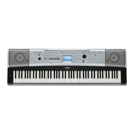
- Page 4 DGX-530/YPG-535 PANEL LAYOUT • Front Panel q [STANDBY/ON] switch @4 Dial w [MASTER VOLUME] control @5 CATEGORY [ ] and [ ] buttons e FILE CONTROL [MENU], [EXECUTE] buttons @6 Number buttons [0]–[9], [+] and [-] buttons r [LYRICS] button @7 [DEMO] button t [SCORE] button @8 [EXIT] button...
- Page 5 DGX-530/YPG-535 • Rear Panel #6 CONTRAST knob #8 SUSTAIN jack #7 USB TO DEVICE terminal #9 PHONES/OUTPUT jack $0 DC IN 12V jack USB TO HOST terminal...
- Page 6 DGX-530/YPG-535 CIRCUIT BOARD LAYOUT & WIRING • Upper case display Speaker Speaker (Tweeter (L)) MVR PNL ENC PNR (Tweeter (R)) 3 15 DJACK • Lower case Speaker Speaker RELAY (Woofer (R)) (Woofer (R)) MK-88L MK-88C MK-88H...
- Page 7 DGX-530/YPG-535 Unit Name Location Part No. Connector assembly Destination Remarks LCD Unit – – Flexible fl at cable DM-CN201 Overall Assembly WN827900 Flexible fl at cable DM-CN301 DJACK-CN301 12P L=120 Overall Assembly WN827800 Flexible fl at cable DM-CN302 DJACK-CN302 5P L=120 Overall Assembly WG317600 Flexible fl...
- Page 8 DGX-530/YPG-535 DISASSEMBLY PROCEDURE Caution: 1) Flat cable’s contacts are visible from the back. Pay attention not to insert and install the cable to the connector inversely. (Fig.1) 2) Be sure to attach the removed filament tape just as it was before removal. Lower Case Assembly (Time required: About 9 minutes) Remove the twenty (20) screws marked [470].
- Page 9 DGX-530/YPG-535 DM Circuit Board (Time required: About 10 minutes) Remove the lower case assembly. (See procedure 1.) Remove the four (4) screws marked [440A]. The DM circuit board can then be removed. (Fig.4) Speaker Speaker (Tweeter(R)) [440A] [440D] [440E] (Tweeter(R)) [440B] [440B] [440C]...
- Page 10 DGX-530/YPG-535 [440H] [440G] [440K] [440I] DJACK Upper Case (Fig.5) [440]: Bind Head Tapping Screw-B 3.0X8 MFZN2W3 (WE774300) ENC Circuit Board MVR Circuit Board (Time required: About 10 minutes) (Time required: About 10 minutes) Remove the lower case assembly. (See procedure 1.) 10-1 Remove the lower case assembly.
- Page 11 DGX-530/YPG-535 PNL Circuit Board (Time required: About 12 minutes) 11-1 Remove the lower case assembly. (See procedure 1.) 11-2 Remove the AM circuit board. (See procedure 5.) 11-3 Remove the ten (10) screws marked [440F]. The PNL circuit board can then be removed. (Fig.8) [440J] [440F] LCD Unit...
- Page 12 DGX-530/YPG-535 RELAY Circuit Board MK-88L, MK-88C, MK-88H Circuit Boards (Time required: About 10 minutes) (Time required: About 16 minutes) 14-1 Remove the lower case assembly. (See procedure 1.) 16-1 Remove the lower case assembly. (See procedure 1.) 14-2 Remove the four (4) screws marked [90]. The RELAY 16-2 Remove the A-1 to B2 white/black keys.
- Page 13 DGX-530/YPG-535 LSI PIN DESCRIPTION ADC084S021CIMM (X6905A00) ADC (Analog to Digital Converter) ..........15 AK4385ET (X6040A00) DAC (Digital to Analog Converter) ..............15 ISP1161A1BD (X5879A00) USB CONTROLLER ................15 S1D13700F01A100 (X5422A00) LCD CONTROLLER ..............14 YMW767-VTZ (X6055A00) CPU (SWL01T) ..................13 µPD789022GB-A15-8E (XZ560100) CPU ..................14 YMW767-VTZ (X6055A00) CPU (SWL01T) DM: IC101 NAME FUNCTION...
- Page 14 DGX-530/YPG-535 S1D13700F01A100 (X5422A00) LCD CONTROLLER DM: IC201 NAME FUNCTION NAME FUNCTION – Ground – Ground AB12 XCD1 Drain output AB11 XCG1 Gate input AB10 Adorress bus RESET# Reset SCANEN Test mode set up input TESTEN HIOVDD – Power supply CLKI Externally sourced system clock COREVDD –...
- Page 15 DGX-530/YPG-535 ISP1161A1BD (X5879A00) USB CONTROLLER DM: IC027 DM: IC301 NAME FUNCTION NAME FUNCTION DGND Digital ground NDP_SEL Indicates to the HC EOT input DGND Digital ground D_SUSPEND DC 'suspend' state output DATA bus D_WAKEUP DC wake-up input GoodLink LED output D_VBUS DC USB input DGND...
- Page 16 DGX-530/YPG-535 IC BLOCK DIAGRAM SN74LV32APWR (X5647A00) SN74AHCT1G08DCKR (X0158A00) NJM4580E(TE2) (X2331A00) Quad 2 Input OR Dual Operational Amplifier 74V1T08CTR (X7542A00) Single 2-Input Positive-AND Gate DM:IC805 DM: IC402 DM: IC103,104 +DC Voltage Output A Supply Inverting Output B Input A Non-Inverting Inverting Input B Input A Non-Inverting...
-
Page 17: Table Of Contents
DGX-530/YPG-535 CIRCUIT BOARDS AM Circuit Board (X9121D0) ....................19 DJACK Circuit Board (X9121D0) ..................... 17 DM Circuit Board (X9734B0) ....................18 ENC Circuit Board (X9121D0) ....................22 MK-88C Circuit Board (X0001A0) .................... 24 MK-88H Circuit Board (X0000A0) .................... 23 MK-88L Circuit Board (X0002A0) ..................... 23 MVR Circuit Board (X9121D0).................... -
Page 18: Dm Circuit Board (X9734B0)
DGX-530/YPG-535 DM Circuit Board to LCD Unit to RELAY-CN01 Component side Pattern side 2NA-WG25920... -
Page 19: Am Circuit Board (X9121D0)
DGX-530/YPG-535 AM Circuit Board to Speaker to Backlight assembly to DM-CN901 to TW (R) to TW (L) (Woofer) PHONES/ OUTPUT DC IN 12V – Component side to MVR-CN601 to PB-CN401 to PSW-CN501 0.5 -1.0mm A nonwoven fabric does not overflow To pile it up in the upper side, it is pasted. -
Page 20: Pnl Circuit Board (X7137D0)
DGX-530/YPG-535 PNL Circuit Board ACMP INTRO/ AUTO ON/OFF ENDING/rit. STYLE SONG REPEAT & LEARN REPEAT METRONOME TEMPO/ ON/OFF LESS LYRICS SCORE PIANO ACMP MENU EXECUTE P.A.T. ON/OFF MUSIC DATABASE FUNC MAIN/ SYNC SYNC TRO/ AUTO FILL STOP START NG/rit. START/ PAUSE STOP PEAT... -
Page 21: Pnr Circuit Board (X7137D0)
DGX-530/YPG-535 Scale: 90/100 PNR Circuit Board BANK RESIST PORTABLE EXIT MEMORY GRAND CATEGORY DOWN VOICE STYLE to DM-CN602 EASY SONG ARRANGER SONG SPLIT DUAL HARMONY VOICE VOICE TYPE HARMONY SPLIT DUAL ON/OFF ON/OFF ON/OFF CATEGORY -/NO +/YES DEMO Component side 2NA-WG25520... -
Page 22: Enc Circuit Board (X9121D0)
DGX-530/YPG-535 ENC Circuit Board MVR Circuit Board MASTER VOLUME Component side Component side to AM-CN204 ROTARY ENCODER PB Circuit Board PSW Circuit Board STANDBY/ON to AM-CN103 Component side Component side PITCH BEND to AM-CN101 TW (L) Circuit Board TW (R) Circuit Board to AM-CN201 to AM-CN202 Component side... -
Page 23: Mk-88H Circuit Board (X0000A0)
DGX-530/YPG-535 MK-88H Circuit Board to MK-88C to RELAY -CN05 Pattern side MK-88L Circuit Board to RELAY-CN03 to MK-88C Pattern side MK-88H: 2LPK8-X0000A0 MK-88L: 2LPK8-X0002A0... -
Page 24: Mk-88C Circuit Board (X0001A0)
DGX-530/YPG-535 MK-88C Circuit Board to MK-88L to RELAY-CN02 to RELAY-CN02 to RELAY-CN04 to MK-88H Pattern side 2LPK8-X0001A0... - Page 25 3) Jigs: Foot switch (FC-4 or FC-5), USB cable, USB memory, USB-MIDI driver (*1) PC (Install a USB-MIDI driver (*1) in PC and finish the THROUGH setup.) *1 Obtain the USB-MIDI driver from CD-ROM (X9318A00) for DGX-530/YPG-535 or Yamaha official website. (URL>>http://www.yamahapkclub.com) HOW TO ENTER THE TEST PROGRAM While pressing the C#2, F2 and G#2 keys, turn the [STANDBY/ON] switch on.
- Page 26 DGX-530/YPG-535 Test Descriptions, Judgment Criteria TEST No. LCD Display 003 Ram Chk1 Checks the RAM that is connected to the CPU. (OK:“Ram OK”, NG:“Ram NG”) The test results appear on the LCD. Check that the LCD displays “Ram OK”. 006 Flash Rom Chk1 Checks the flash ROM that is connected to CPU bus.
- Page 27 DGX-530/YPG-535 Test Descriptions, Judgment Criteria TEST No. LCD Display 033 Pitch Bend Chk Checks the pitch bend wheel. (First, it checks if the center position of the wheel is correct or not.) Check that the C3 note is output when rotating the [PITCH BEND] wheel to minimum and the C4 note is output when rotating it to maximum.
- Page 28 DGX-530/YPG-535 Table 1 SW Name Display Note No. DIAL UP Dial Up DIAL DOWN Dial Down FILE MENU File Menu FILE EXCUTE File Excute P.A.T. P. A.T. Music Data Base MusicDataBase FUNCTION Function LYRICS Lyrics SCORE Score Chord Fingering Chord Finger LESSON L Lesson L LESSON R...
- Page 29 DGX-530/YPG-535 INITIALIZATION This function erases all backup data in the instrument’s fl ash memory and restores the initial default settings. The following initialization procedures are provided. Backup Clear To clear data backed up to the internal fl ash memory (DM circuit board: IC803)—panel user setting, registration memory, user songs, style file—turn the power on by pressing the [STANDBY/ON] switch while holding the highest white key on the keyboard.
- Page 30 DGX-530/YPG-535 USER DATA BACKUP To backup user data to an external device, use a USB fl ash memory. Refer to the following for the data you can backup using it. List of data that can be backed up • User Songs • ...
- Page 31 DGX-530/YPG-535 Formatting USB Flash Memory New USB flash memory must be formatted before they can be used by this instrument. Press the [EXECUTE] button again, or CAUTION the [+] button, and the format operation • If you format a USB flash memory that already contains data, all of will begin.
- Page 32 DGX-530/YPG-535 Saving Data Three types of data are saved to one “User File” by this operation: user song, style file, and registration mem- ory data. When you save a user song the style file and registration memory are also saved automatically. Make sure that a properly formatted USB flash memory has been properly connected to the instrument’s USB TO...
- Page 33 DGX-530/YPG-535 Loading User Files and Style Files User files, style files, and styles residing on a USB flash memory can be loaded into the instrument. The style file will be loaded into style number 161. If the required style file has already been transferred to the instrument from a computer using the Musicsoft Downloader application, start from step 2, below.
- Page 34 DGX-530/YPG-535 MIDI IMPLEMENTATION CHART YAMAHA [ Portable Grand ] Date:10-OCT-2007 Model DGX-530/YPG-535 MIDI Implementation Chart Version:1.0 Transmitted Recognized Remarks Function... Basic Default 1 - 16 1 - 16 Channel Changed Default Mode Messages Altered ************** Note 0 - 127 0 - 127...
- Page 35 DGX-530/YPG-535 MIDI DATA FORMAT 7 Effect map * When a Type LSB value is received that corresponds to no effect type, a value corresponding to the effect type (coming the closest to the specifi ed value) is automatically set. * The numbers in parentheses in front of the Effect Type names correspond to the number indicated in the display. ¶ REVERB TYPE LSB TYPE No Effect (01)Hall1 (02)Hall2 (03)Hall3 Room (04)Room1 (05)Room2 Stage (06)Stage1 (07)Stage2 Plate (08)Plate1 (09)Plate2 005...127 No Effect ¶ CHORUS TYPE LSB TYPE 000...063 No Effect Thru Chorus (02)Chorus2 Celeste (01)Chorus1...
- Page 36 DIGITAL KEYBOARD PARTS LIST PARTS LIST CONTENTS OVERALL ASSEMBLY ............. 2 STAND ASSEMBLY ............5 LOWER CASE ASSEMBLY ..........6 KEYBOARD ASSEMBLY ..........8 ELECTRICAL PARTS ..........10–16 Notes : DESTINATION ABBREVIATIONS A : Australian model M : South African model B : British model O : Chinese model C : Canadian model...
-
Page 37: Overall Assembly
DGX-530/YPG-535 OVERALL ASSEMBLY Upper case assembly Music rest U70a U130 U120 U170 U140 U160 U70b U170 U80c U70a U100 U160 U80b U130 U80a U160 U170 U110 U150 U130 U170 U160 U155 U145 U90c 340b U90b 340a Wheel assembly U150 U90a 290a U110 250a... - Page 38 DGX-530/YPG-535 PART NO. DESCRIPTION 部 品 名 REMARKS REF NO. QTY RANK OVERALL ASSEMBLY 総 組 立 DGX-530/YPG-535 Overall Assembly 総 組 立 DGX-530U,C,E,B,Y (WM36610) Overall Assembly 総 組 立 YPG-535 U,C,E,B (WM36620) WM429400 Upper Case Assembly 上 ケ ー ス A s s y...
- Page 39 DGX-530/YPG-535 PART NO. DESCRIPTION 部 品 名 REMARKS REF NO. QTY RANK WE987400 Bind Head Tapping Screw-B 3.0X12 MFZN2W3 B タ イ ト + B I N D WF154100 Bind Head Tapping Screw-B 4.0X16 MFZN2W3 B タ イ ト + B I N D WD365700 Sponge ス...
-
Page 40: Stand Assembly
DGX-530/YPG-535 STAND ASSEMBLY 250b 250a 250b 270b 250b 250b 270a 250a 270b 270a PART NO. DESCRIPTION 部 品 名 REMARKS REF NO. QTY RANK STAND ASSEMBLY ス タ ン ド A s s y DGX-530/YPG-535 Stand Assembly ス タ ン ド A s s y... -
Page 41: Lower Case Assembly
DGX-530/YPG-535 LOWER CASE ASSEMBLY Keyboard assembly See page 8. 100a 100b Lower case sub assembly... - Page 42 DGX-530/YPG-535 PART NO. DESCRIPTION 部 品 名 REMARKS REF NO. QTY RANK LOWER CASE ASSEMBLY 下 ケ ー ス A s s y DGX-530/YPG-535 Lower Case Assembly 下 ケ ー ス A s s y (WM43010) WF839900 Lower Case Sub Assembly 下...
-
Page 43: Keyboard Assembly
DGX-530/YPG-535 KEYBOARD ASSEMBLY Lower case... - Page 44 DGX-530/YPG-535 PART NO. DESCRIPTION 部 品 名 REMARKS REF NO. QTY RANK KEYBOARD ASSEMBLY 1 6 N − A 8 8 鍵 盤 DGX-530/YPG-535 Keyboard Assembly 16N-P A88 P2M I 1 6 N − A 8 8 鍵 盤 (WM43080) V 7 3 8 0 3 0 0 White Key 16N-P CEGB-P 白...
-
Page 45: Electrical Parts
DGX-530/YPG-535 ELECTRICAL PARTS AM/DJACK/ENC/MVR/PB/PSW/TW PART NO. DESCRIPTION 部 品 名 REMARKS REF NO. QTY RANK ELECTRICAL PARTS 電 気 部 品 DGX-530/YPG-535 WN145800 Circuit Board A M シ ー ト (WK92550)(X9121D0) WN145900 Circuit Board DJACK D J A C K シ ー ト (WK92550)(X9121D0) WN146300 Circuit Board E... - Page 46 DGX-530/YPG-535 AM/DJACK/ENC/MVR/PB/PSW/TW PART NO. DESCRIPTION 部 品 名 REMARKS REF NO. QTY RANK -215 VR168300 Monolithic Mylar Capacitor ECQ-V1H104JL3 積 層 マ イ ラ ー コ ン C216 UR837330 Electrolytic Cap. 33.00 16.0V RX TP ケ ミ コ ン C216 V 3 5 0 8 3 0 0 Electrolytic Cap.
- Page 47 DGX-530/YPG-535 AM/DJACK/ENC/MVR/PB/PSW/TW and DM PART NO. DESCRIPTION 部 品 名 REMARKS REF NO. QTY RANK L306 VB835000 Coil FL05RD200AT 20uH コ イ ル 2 0 U L306 VT279200 Coil DX001-20UH 20uH コ イ ル 2 0 U 天 津 製 R101 HF455100 Carbon Resistor 100.0 1/4 J AX TP...
- Page 48 DGX-530/YPG-535 PART NO. DESCRIPTION 部 品 名 REMARKS REF NO. QTY RANK -223 US062100 Ceramic Capacitor-SL(chip) 100P 50V J RECT. チ ッ プ セ ラ( S L ) C301 US145100 Ceramic Capacitor-F (chip) 0.1000 25V Z RECT. チ ッ プ セ ラ( F ) -303 US145100 Ceramic Capacitor-F (chip) 0.1000 25V Z RECT.
- Page 49 DGX-530/YPG-535 PART NO. DESCRIPTION 部 品 名 REMARKS REF NO. QTY RANK IC301 X5879A00 IC ISP1161A1BD_118-PB I C USB CONTROLLER IC302 X7414A00 IC R5520H001A-T1-F I C USB HIGH SIDE SWITCH IC401 X6040A00 IC AK4385ET I C DAC IC402 X2331A00 IC NJM4580E(TE2) I...
- Page 50 DGX-530/YPG-535 DM and MK-88C and MK-88H and MK-88L and PNL/PNR PART NO. DESCRIPTION 部 品 名 REMARKS REF NO. QTY RANK R408 RD355180 Carbon Resistor (chip) 180.0 63M J RECT. チ ッ プ 抵 抗 R409 RD355180 Carbon Resistor (chip) 180.0 63M J RECT.
- Page 51 DGX-530/YPG-535 PNL/PNR and RELAY PART NO. DESCRIPTION 部 品 名 REMARKS REF NO. QTY RANK VB941200 Diode 1SS133,1SS176 TE ダ イ オ ー ド VB941200 Diode 1SS133,1SS176 TE ダ イ オ ー ド VV437800 Diode 1N4148(DO-34) ダ イ オ ー ド...
- Page 52 DGX-530/YPG-535 BLOCK DIAGRAM DGX-530/YPG-535 SUSTAIN TO HOST CONTRAST BACK LIGHT VR301 PITCH BEND JK301 JK303 JK302 DJACK VR401 STANDBY/ON DISPLAY 320 X 240 SW501 CN301(12P), CN302 (5P) CN501(4P) CN103(3P) CN102(2P) CN101(4P) CN301(12P), CN302 (5P) CN201(14P) +29V XD0-3 IC102(3P) YD,LP DC/DC 6MHz +21~27V XCSL,WF...
- Page 53 <Page1> DGX-530/YPG-535 DGX-530/YPG-535 OVERALL CIRCUIT DIAGRAM 1/2 (AM, DJACK, DM, MVR, PB, PSW, TW) RH5RZ25CA-T1-F (X3679A00) 1SS372 (V9424900) REGULATOR +2.5V DIODE ARRAY DM: IC901 DM: DA301–304 DC/DC 1: ANODE1 CONVERTER 1. GND 2: CATHODE2 2. INPUT 3: CATHODE1, . OUTPUT ANODE2 to RELAY-CN01 <Page2 L-3>...
- Page 54 <Page2> DGX-530/YPG-535 DGX-530/YPG-535 OVERALL CIRCUIT DIAGRAM 2/2 (ENC, MK-88C, MK-88H, MK-88L, PNL, PNR, RELAY) RELAY REPEAT& LEARN LESSON L TEMPO/TAP MEMORY 3 MENU P.A.T FUNCTION PAUSE EXECUTE LYRICS LESSON R MEMORY MEMORY 4 A-B REPEAT START/STOP START/ STOP SCORE START MEMORY 1 MEMORY 5 P.A.T.