Table of Contents
Advertisement
Quick Links
Advertisement
Table of Contents
Troubleshooting

Related Manuals for Panasonic VIERA Link SC-ZT2EE


Summary of Contents for Panasonic VIERA Link SC-ZT2EE
- Page 1 PSG1005041CE Home Theater Audio System SC-ZT2EE Model No. SC-ZT2GS SU-ZT2EE SU-ZT2GS SB-ZT2EE SB-ZT2GS Product Color: (K)...Black Type (SC-ZT2/SU-ZT2) (K1)...Black Type (SB-ZT2) © Panasonic Corporation 2010. All rights reserved. Unauthorized copying and distribution is a violation of law.
-
Page 2: Table Of Contents
TABLE OF CONTENTS PAGE PAGE 1 Safety Precautions -----------------------------------------------3 18 Schematic Diagram ------------------------------------------- 149 1.1. General Guidelines ----------------------------------------3 18.1. Main Unit (SU-ZT2) ------------------------------------149 1.2. Before Repair and Adjustment--------------------------4 18.2. Speaker Unit (SB-ZT2) -------------------------------- 163 19 Printed Circuit Board----------------------------------------- 169 1.3. Caution for Fuse Replacement -------------------------4 1.4. -
Page 3: Safety Precautions
1 Safety Precautions 1.1. General Guidelines 1. When servicing, observe the original lead dress. If a short circuit is found, replace all parts which have been overheated or damaged by the short circuit. 2. After servicing, see to it that all the protective devices such as insulation barriers, insulation papers shields are properly installed. -
Page 4: Before Repair And Adjustment
1.2. Before Repair and Adjustment Disconnect AC power, discharge Power Supply Capacitors for : Main Unit (SU-ZT2) (C5501, C5502, C5509) through a 10Ω, 1W resistor to ground. Speaker Unit (SB-ZT2) (C5700, C5701, C5703, C5704) through a 10Ω, 1W resistor to ground. DO NOT SHORT-CIRCUIT DIRECTLY (with a screwdriver blade, for instance), as this may destroy solid state devices. - Page 5 1.5.1. Main Unit (SU-ZT2) Safety Ref. No. Part No. Part Name & Description Remarks RGR0393A-K REAR PANEL RGR0393A-M REAR PANEL RKM0613-K TOP CABINET K2CA2CA00031 AC CORD K2CP2CA00001 AC CORD K2CQ2CA00007 AC CORD K2CZ3YY00005 AC CORD VQT2R71 O/I (En) VQT2U14 O/I (Ru/Ur) VQT2U15 PCB3 REPX0678D...
-
Page 6: Warning
2 Warning 2.1. Prevention of Electro Static Discharge (ESD) to Electrostatically Sensi- tive (ES) Devices Some semiconductor (solid state) devices can be damaged easily by static electricity. Such components commonly are called Elec- trostatically Sensitive (ES) Devices. Examples of typical ES devices are integrated circuits and some field-effect transistors and semiconductor “chip”... -
Page 7: Service Caution Based On Legal Restrictions
2.2. Service caution based on Legal restrictions 2.2.1. General description about Lead Free Solder (PbF) The lead free solder has been used in the mounting process of all electrical components on the printed circuit boards used for this equipment in considering the globally environmental conservation. The normal solder is the alloy of tin (Sn) and lead (Pb). -
Page 8: Service Navigation
3 Service Navigation 3.1. Service Information This service manual contains technical information which will allow service personnel’s to understand and service this model. Please place orders using the parts list and not the drawing reference numbers. If the circuit is changed or modified, this information will be followed by supplement service manual to be filled with original service manual. -
Page 9: Specifications
4 Specifications SPEAKER GENERAL* Power supply AC 110 to 240 V, 50/60 Hz Power consumption 20 W 4.1. Main Unit (SU-ZT2) Wireless link standby 0.8 W In standby condition 0.15 W Dimensions (WxHxD) 290mm x 1231mm x 290mm PRE AMPLIFIER SECTION Mass [Weight] Approx. -
Page 10: Location Of Controls And Components
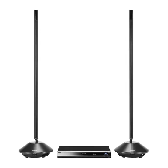
5 Location of Controls and Components 5.1. Main Unit (SU-ZT2) -
Page 11: Speaker Unit (Sb-Zt2)
5.2. Speaker Unit (SB-ZT2) 5.3. Remote Control... -
Page 12: Installation
6 Installation... -
Page 13: Basic Connections
6.1. Basic Connections 6.1.1. Connecting equipment with HDMI terminal (TV, DVD recorder, etc.) - Page 14 6.1.2. Connecting equipment without HDMI terminal (DVD player, VCR, etc.)
- Page 15 6.1.3. Connecting STB etc. and audio terminals (DVD player, etc.)
- Page 16 6.1.4. Other connections...
-
Page 17: Ac Power Supply Connection
6.2. AC power supply connection... -
Page 18: Speaker Setting (Sb-Zt2)
7 Speaker setting (SB-ZT2) 7.1. Setting the speakers (Front and Surround speakers) -
Page 20: Setting Surround Speakers
7.2. Setting surround speakers... -
Page 21: Initialize The Speaker Setting
7.3. Initialize the Speaker Setting About the method of initializing the setting of the speaker. Please initialize it when the main body of the speaker is changed or it added. Please set the speaker after ID is reset. Preparation: Please connect the power supply code of the speaker. Please confirm the power supply of the speaker cuts. -
Page 22: Self-Diagnostic And Special Mode Setting
8 Self-diagnostic and special mode setting This unit is equipped with the self-diagnostic display function, which alarms faulty operation with error code. Use this function during servicing. 8.1. Activating Service Mode This mode can be used during servicing. 1. Plug the AC adapter to the power source. Press and hold down the [VOL +] button and the [VOL -] button, and then press the [POWER ] button at the same time. -
Page 23: Inspection Mode
Fig. 3 FL display Symptom Cause and Remedy F61/OVERLOAD Speaker short, amplifier failure, electrical over- Speaker short and failure in power amplifier, pre-amplifier load etc. circuits. Check for faulty parts and replace with new parts if necessary. Humidity protection activated FANLOCK Fan stopped Failure fan and fan control circuits. -
Page 24: Returning To Normal Display
Remote Control Test Mode Function and settings Selector Sound Mode Other settings Vol/Tone TEST AUX 4 (Analog) — All CH output mode -18dB/0dB TV (OPT1) STEREO Balance is set to leftmost. -18dB/0dB TV (OPT1) STEREO Balance is set to rightmost. -18dB/0dB VIRTUAL AUX 4 (Analog) -
Page 25: Troubleshooting
9 Troubleshooting 9.1. HDMI Checking Method 1. Connection of HDMI system 2. Check of HDMI Sound a. Using the [DVD AUDIO TEST DISC V-612] and DVD-VIDEO disc with Dolby Digital signal. b. [DVD AUDIO TEST DISC V-612] - Track No. 92 (96kHz, 5.1ch). Track No. 40 (Zero) Check the Level and Noise, output from L / C / R / SL / SR / SW / speaker or pin. - Page 26 Comfirmed that there are neither distortion nor a noise on the screen. • If it is a picture quality equal when DVD was connected directly to TV, it is OK 1. Connect directly DVD player to TV. 2. Connect DVD player to set then connect it to TV. 3.
-
Page 27: Troubleshooting Flow Chart
9.2. Troubleshooting Flow Chart 9.2.1. Main Unit (SU-ZT2) Power Supply No power supply Primary Fuse (F701 check Main P.C.B Power circuit check D5502 Pin IC5501 Pin IC5502 Pin Main P.C.B PC5501 Pin Micro-processor IC IC8001 Power Supply line checking: Reset IC IC8003 D5505 IC5571 Pin... - Page 28 9.2.2. Speaker Unit (SB-ZT2)
- Page 29 9.2.3. Speaker Unit (SB-ZT2) - Wireless Link...
-
Page 31: Disassembly And Assembly Instructions
10 Disassembly and Assembly Instructions Caution Note: • This section describes the disassembly and/or assembly procedures for all major printed circuit boards & main compo- nents for the unit. (You may refer to the section of “Main components and P.C.B Locations” as described in the service manual) •... -
Page 33: Main Parts Location Diagram
10.1. Main Parts Location Diagram 10.1.1. Main Unit (SU-ZT2) - Page 34 10.1.2. Speaker Unit (SB-ZT2)
-
Page 35: Disassembly Flow Chart
10.2. Disassembly flow chart The following chart is the procedure for disassembling the casing and inside parts for internal inspection when carrying out the ser- vicing. To assemble the unit, reverse the steps shown in the chart below. 10.2.1. Main Unit (SU-ZT2) - Page 36 10.2.2. Speaker Unit (SB-ZT2)
-
Page 37: Main Unit (Su-Zt2)
10.3. Main Unit (SU-ZT2) Step 3 : Lift up the rear part of the Top Cabinet and remove it in order as arrows shown. 10.3.1. Disassembly of Top Cabinet Caution : During assembling, ensure that the Top Cabinet is fully inserted into the Front Cabinet. Step 1 : Remove 2 screws. - Page 38 10.3.2. Disassembly of HDMI P.C.B. Step 6 : Lift up to remove the HDMI P.C.B. and the HDMI Sup- port Chassis as arrow shown. • Refer to “Disassembly of Top Cabinet”. Caution : During assembling of the HDMI P.C.B., ensure that the HDMI Support Chassis is properly catched onto Step 1 : Remove 2 screws.
- Page 39 10.3.3. Disassembly of DSP P.C.B. Step 8 : Lift up to remove the HDMI P.C.B. from the HDMI Sup- port Chassis. • Refer to “Disassembly of Top Cabinet”. Step 1 : Detach the 14P FFC at the connector (CN1002) on the DSP P.C.B.
- Page 40 10.3.4. Disassembly of Rear Panel Step 3 : Release the claws of the P.C.B. Support. Step 4 : Remove the DSP P.C.B. • Refer to “Disassembly of Top Cabinet”. Caution : During assembling, ensure the DSP P.C.B. is • Refer to (Step 1) - (Step 6) of “Disassembly of HDMI P.C.B.”. seated properly.
- Page 41 10.3.5. Disassembly of Wireless TX P.C.B. Step 3 : Remove the Rear Panel. and TX Module P.C.B. • Refer to “Disassembly of Top Cabinet”. Step 1 : Detach 9P FFC at the connector (CN4702) on the Wireless TX P.C.B. Step 2 : Remove 1 screw. Caution : Do not misplace the Ferrite Core when detaching the FFC.
- Page 42 Step 4 : Remove the Wireless TX P.C.B. and the TX Module Step 5 : Remove the TX Module P.C.B. from the Wireless TX P.C.B. as arrow shown. P.C.B. Caution : Ensure that the Wireless TX P.C.B. and TX Mod- ule P.C.B.
- Page 43 10.3.6. Disassembly of Main P.C.B. Step 7 : Detach 12P FFC at the connector (CN4221) on the Main P.C.B. • Refer to “Disassembly of Top Cabinet”. Step 8 : Detach 14P FFC at the connector (CN4102) on the • Refer to (Step 1) of “Disassembly of Rear Panel”. Main P.C.B.
- Page 44 Step 9 : Release the claws of the P.C.B. Support. Step 11 : Gently detach one side of the Rear Panel. Step 10 : Remove the DSP P.C.B. Caution : Ensure the Rear Panel is fitted properly during assembling. Step 12 : Remove the Main P.C.B.
- Page 45 10.3.7. Disassembly of Front Cabinet Caution : During assembling, ensure that the Main P.C.B. is fitted properly onto locators. • Refer to “Disassembly of Top Cabinet”. • Refer to (Step 1) - (Step 4) of “Disassembly of Wireless TX P.C.B. and TX Module P.C.B.”. Step 1 : Remove 1 screw.
- Page 46 10.3.8. Disassembly of Panel P.C.B. and Step 3 : Lift both sides of the Front Cabinet to release from the guides and release the 3 catches at the bottom of the Main Power SW P.C.B. Unit. • Refer to “Disassembly of Top Cabinet”. Step 4 : Remove the Front Cabinet.
- Page 47 Step 5 : Remove the Panel P.C.B. and Power SW P.C.B. Caution : During assembling, ensure that the Power SW P.C.B. and Panel P.C.B. are fitted properly onto the loca- tors. Note : During assembling of the Power SW P.C.B. and Panel P.C.B., ensure that the 3P wire is positioned above the Wireless Holder as diagram shown.
-
Page 48: Speaker Unit (Sb-Zt2)
10.4. Speaker Unit (SB-ZT2) 10.4.1. Disassembly of Woofer Block Step 1 : Lay the Speaker Unit on a support block as shown. Step 2 : Remove 9 screws. Step 3 : Remove 3 screws. - Page 49 Step 4 : Remove the Weight.
- Page 50 Step 5 : Remove 10 screws.
- Page 51 Step 6 : Remove 1 screw. Step 7 : Push Power Button to “On” position. Caution : Ensure the Power Button is push back to “Off” position when disassembly of Bottom Cabinet is completed.
- Page 52 Step 8 : Remove the Bottom Cabinet. Caution : Support by holding onto the Woofer Block firmly after removal of the Bottom Cabinet to prevent it being detached from the Tweeter Block accidentally.
- Page 53 Step 9 : Detach 2P cable at the connector (CN6052) on the Extent P.C.B. Step 10 : Using a Jig (RFKZ0535), hook on to detach antenna wire at the RF connector (ET6002) on the Extent P.C.B. Caution : The RF connector (ET6002) is fragile, take extra care not to damage it during disassembling. Caution 1 : During assembly, position the antenna wire around the connector (CN6052) and the locator and place it into the slot.
- Page 54 Step 11 : Remove 2 screws. Step 12 : Lift up to remove Arm Cover A.
- Page 55 Caution 1 : Align the Tip of Arm Cover A to the Tip of the Arm during assembly of Arm Cover A. Caution 2 : Ensure the wires that are clamped onto the Arm are kept within Arm Cover A when assembling of Arm Cover Step 13 : Remove 1 screw.
- Page 56 Step 14 : Tilt the Woofer Block in order as arrows shown to detach it from the Tweeter Block.
- Page 57 10.4.2. Disassembly of Middle Cabinet Assembly • Refer to “Disassembly of Woofer Block”. Step 1 : Remove 7 screws.
- Page 58 Step 2 : Lift up to remove Middle Cabinet Assembly from the Woofer Cover Assembly. Caution 1 : Light Panel easily drop off, take extra care not to misplace it. Caution 2 : Replace the EPT Sealer if it is torn. Caution 3 : Ensure Middle Cabinet Assembly is properly fitted onto the arm slot and locators during assembling.
- Page 59 10.4.3. Disassembly of Extent P.C.B. • Refer to (Step 1) - (Step 10) of “Disassembly of Woofer Block”. Step 1 : Remove 1 screw. Step 2 : Detach 2P cable at the connector (CN6051) on the Extent P.C.B. Step 3 : Using a Jig (RFKZ0535), hook on to detach coaxial cable at the RF connector (ET6001) on the Extent P.C.B. as shown. Step 4 : Remove the Extent P.C.B.
- Page 60 Caution 1 : During assembly, position the coaxial cable around the connector (CN6051) and place it into both slots. Caution 2 : Position the 2P cable into both slot above the coaxial cable.
- Page 61 10.4.4. Disassembly of SMPS P.C.B. and AC Inlet P.C.B. • Refer to “Disassembly of Woofer Block”. • Refer to “Disassembly of Middle Cabinet Assembly”. Step 1 : Detach 10P cable at the connector (CN5802) on the SMPS P.C.B. Step 2 : Remove 3 screws. Step 3 : Remove 1 screw.
- Page 62 Caution : During assembling, ensure that the SMPS P.C.B. is properly fitted onto the locators of the Middle Cabinet Assembly.
- Page 63 Step 4 : Turn and place the SMPS P.C.B. aside as arrow shown. Step 5 : Remove 1 screw. Step 6 : Remove the Support P.C.B. with tweezers. Caution : During assembling, ensure that the Support P.C.B. is properly fitted onto the locators of the Middle Cabinet Assembly.
- Page 64 Step 7 : Using tweezers, gently push the AC Inlet P.C.B. until the AC Inlet is released from the Middle Cabinet Assembly, then lift up to remove both AC Inlet P.C.B. and SMPS P.C.B. Caution : Ensure that the wires (Black and Red) are dressed to the right side of the boss during assembling of the AC Inlet P.C.B.
- Page 65 Caution 1 : Ensure that AC Inlet P.C.B. is properly fitted onto the locator of the Middle Cabinet Assembly during assem- bling. Caution 2 : Ensure that the AC Inlet is fully inserted and protruding slightly from the exterior of the Middle Cabinet Assem- bly when completed.
- Page 66 10.4.5. Replacement of IC5701 • Refer to “Disassembly of SMPS P.C.B. and AC Inlet P.C.B.”. Caution : Handle the SMPS P.C.B. with care due to its high temperature after prolonged use. Avoid touching the heatsink as it may lead to injuries. Step 1 : Desolder pins of IC5701 on the solder side of SMPS P.C.B.
- Page 67 Step 3 : Remove the heatsink with the IC5701.
- Page 68 Step 4 : Remove 1 screw. Step 5 : Remove IC5701 from the heatsink.
- Page 69 • Assembly of IC5701 Step 1 : Apply grease on the heatsink. Step 2 : Place IC5701 against the heatsink. Step 3 : Fix 1 screw. Caution : Ensure that IC5701 is firmly fixed onto the heatsink.
- Page 70 Step 4 : Place the heatsink with the IC5701 onto the SMPS P.C.B.
- Page 71 Step 5 : Solder pins of IC5701 on the solder side of SMPS P.C.B. Step 6 : Solder pins of heatsink on the solder side of SMPS P.C.B. Caution : Ensure that pins of IC5701 and heatsink are properly located and soldered onto the SMPS P.C.B.
- Page 72 10.4.6. Replacement of Diode (D5802) • Refer to “Disassembly of SMPS P.C.B. and AC Inlet P.C.B.”. Caution : Handle the SMPS P.C.B. with care due to its high temperature after prolonged use. Avoid touching the heatsink as it may lead to injuries. Step 1 : Remove 1 screw.
- Page 73 Step 2 : Desolder pins of Diode (D5802) on the solder side of SMPS P.C.B. Step 3 : Remove the Diode (D5802).
- Page 74 • Assembly of Diode (D5802) Step 1 : Apply grease on the heatsink. Step 2 : Place Diode (D5802) on the SMPS P.C.B. against the heatsink. Caution : Ensure that Diode (D5802) is firmly fixed onto the heatsink.
- Page 75 Step 3 : Solder pins of Diode (D5802) on the solder side of the SMPS P.C.B. Caution : Ensure that pins of Diode (D5802) are properly located and soldered onto the SMPS P.C.B. Step 4 : Fix 1 screw.
- Page 76 10.4.7. Disassembly of D-Amp P.C.B. • Refer to “Disassembly of Woofer Block”. • Refer to “Disassembly of Middle Cabinet Assembly”. • Refer to (Step 1) of “Disassembly of SMPS P.C.B. and AC Inlet P.C.B.”. Caution : D-Amp P.C.B. is replaced as a module. Step 1 : Remove 2 screws.
- Page 77 Caution 1 : Replace the Sealer if it is torn. Caution 2 : When connecting 2P cable to the connector (CNB6004), ensure the 2P cable is dressed behind the RX Module P.C.B. and placed onto the slot. Step 5 : Remove the Sound Absorber.
- Page 78 Step 6 : Detach the White/Blue (+) and White (-) speaker wires. Step 7 : Remove the speaker wires from the slot in the Middle Cabinet Assembly. Step 8 : Remove the D-Amp P.C.B. Caution 1 : During assembling, ensure that the D-Amp P.C.B. is properly fitted onto the locators of the Middle Cabinet Assembly.
- Page 79 10.4.8. Disassembly of RX Module P.C.B. • Refer to “Disassembly of Woofer Block”. • Refer to “Disassembly of Middle Cabinet Assembly”. • Refer to (Step 1) - (Step 4) of “Disassembly of D-Amp P.C.B.”. Caution : RX Module P.C.B. is replaced as a module. Pairing is necessary after replacement. Step 1 : Remove the speaker wires from the slot in the Middle Cabinet Assembly.
- Page 80 Step 2 : Flip and place the D-Amp P.C.B. as arrow shown. Step 3 : Using a Jig (RFKZ0535), hook on to detach coaxial cable at the connector (U18) on the RX Module P.C.B. Caution : The connector (U18) is fragile, take extra care not to damage it during disassembling. Step 4 : Release catches on the P.C.B.
- Page 81 10.4.9. Disassembly of Input P.C.B. • Refer to “Disassembly of Woofer Block”. • Refer to “Disassembly of Middle Cabinet Assembly”. • Refer to (Step 1) - (Step 4) of “Disassembly of SMPS P.C.B. and AC Inlet P.C.B.”. • Refer to (Step 1) - (Step 7) of “Disassembly of D-Amp P.C.B.”. •...
- Page 82 Step 4 : Remove 3 screws. Step 5 : Remove the Power Button.
- Page 83 Caution : Ensure that the Power Button Switch is pushed down to ‘On’ position before fixing the Power Button. Step 6 : Hold on to the P.C.B. Holder to remove the Input P.C.B. as arrow shown. Caution 1 : During assembling of the Input P.C.B., ensure that the TEST Terminal Jack is properly slot into the guide hole in the Middle Cabinet Assembly.
- Page 84 10.4.10. Disassembly of Port Assembly (A , B) and Port Assembly (C, D) • Refer to “Disassembly of Woofer Block”. Step 1 : Remove 4 screws. Step 2 : Remove the wires from the slots in the Middle Cabinet Assembly. Step 3 : Lift up to remove the Port Assembly.
- Page 85 Step 4 : Detach Port Assembly (A, B) from Port Assembly (C, D). Caution 1 : During assembling of Port Assembly, align the guide on Port Assembly (C, D) to the guide slot in Port Assem- bly (A, B). Caution 2 : During replacement of the Port Noise Absorber, use the rib of Port Assembly (C, D) as reference when pasting the Port Noise Absorber.
- Page 86 10.4.11. Disassembly of Woofer Speaker (SP1) • Refer to “Disassembly of Woofer Block”. • Refer to (Step 1) - (Step 3) of “Disassembly of Port Assembly (A , B) and Port Assembly (C, D)”. Step 1 : Remove the Sound Absorber. Step 2 : Detach the White/Blue (+) and White (-) speaker wires.
- Page 87 Step 3 : Remove 4 screws. Step 4 : Lift up to remove Woofer Speaker (SP1).
- Page 88 10.4.12. Disassembly of Arm Unit • Refer to “Disassembly of Woofer Block”. Step 1 : Remove 2 screws. Step 2 : Lift and flip over the Arm as arrow shown. Caution : Take extra care not to damage the wires while flipping the Arm.
- Page 89 Step 3 : Cut the 4 wire clampers to remove the Arm. Caution : During assembling, replace with new wire clampers and ensure that the wire clampers are tightened such that the wires are firmly located in the Arm. Step 4 : Remove 2 screws. Step 5 : Detach Arm Cover B from the Arm.
- Page 90 10.4.13. Disassembly of Prepared Net Assembly • Refer to “Disassembly of Woofer Block”. • Refer to (Step 1) - (Step 2) of “Disassembly of Arm Unit”. Step 1 : Remove 1 screw. Caution: During assembling, do not tighten the screw too tight to avoide the screw hole becomes bigger. Step 2 : Remove the Pipe Bottom Cover.
- Page 91 Step 3 : With the Prepared Net Assembly facing up, insert a minus screwdriver behind the net frame folded part and apply gentle force to push out the Prepared Net Assembly as arrows (1) and (2) shown. Step 4 : Apply gentle force to remove the Prepared Net Assembly completely from the Pipe. Caution : Take extra care not to tear or damage the Net during removal and assembling of the Prepared Net Assembly.
- Page 92 10.4.14. Disassembly of Antenna Cover Assembly • Refer to “Disassembly of Woofer Block”. • Refer to (Step 1) - (Step 2) of “Disassembly of Arm Unit”. • Refer to “Disassembly of Prepared Net Assembly”. Step 1 : Remove 2 screws. Step 2 : Remove the Antenna Cover Assembly.
- Page 93 Step 3 : Using tweezers, lift up the front part of the Antenna Front Ornament slightly as arrow (1) shown. Step 4 : Release the 6 catches on the Antenna Front Ornament gradually in order as arrows (2), (3) and (4) shown. Step 5 : Remove Antenna Front Ornament.
- Page 94 Step 6 : Remove 4 screws. Step 7 : Peel off the himelon. Caution : During assembling, replace the himelon if it is torn. Step 8 : Lift up to detach Antenna Cover A from Antenna Cover B. Caution : Using the 4 catches on Antenna Cover A and the guide on Antenna Cover B, ensure that Antenna Cover A and Antenna Cover B are fitted firmly together during assembling.
- Page 95 10.4.15. Disassembly of Antenna Wire • Refer to “Disassembly of Woofer Block”. • Refer to (Step 1) - (Step 2) of “Disassembly of Arm Unit”. • Refer to “Disassembly of Prepared Net Assembly”. • Refer to (Step 1) - (Step 2) of “Disassembly of Antenna Cover Assembly”. Step 1 : Detach the Wire Protector from the Pipe Assembly and remove it from the wires.
- Page 96 Step 2 : Lift up the Blind Sheets A, B and C, until the Sound Absorber on each side is in sight. Step 3 : Remove the Sound Absorbers. Caution : During assembling, replace the Blind Sheet if it is torn. Caution : Ensure that all holes are fully covered by the Blind Sheets.
- Page 97 Step 4 : Remove 5 screws. Caution : Fix 5 screws in order during assembling. Caution : Use a minus screwdriver to scrape off the burr around the screw hole before disassembling and assembling of the Tweeter Base Frame.
- Page 98 Step 5 : Gradually remove the Tweeter Base Frame from the Pipe Assembly. Caution 1 : Gradually insert the wires into the Pipe while the Tweeter Base Frame is being removed. Caution 2 : Take extra care not to damage the wires during assembling and removal of the Tweeter Base Frame. Caution 3 : Take extra care not to damage the antenna during assembling and removal of the Tweeter Base Frame.
- Page 99 Caution 5 : During assembling, gradually insert the Tweeter Base Frame by using a ball point pen (with the ball point hid- den) to push at the 4 designated gray areas.
- Page 100 Caution 6 : During assembling, after the Tweeter Base Frame inserted into the Pipe, pull out the wires with tweezers. Caution 7 : During assembling of the Tweeter Base Frame, ensure that the screw holes of the Tweeter Base Frame are respectively aligned with the screw holes in the interior of the Pipe to allow proper fixation of screws.
- Page 101 Step 6 : Remove 1 screw. Step 7 : Remove the Antenna Holder. Caution : Ensure that the 2 guides on the Antenna Holder are properly located into the Tweeter Base Frame during assem- bling.
- Page 102 Step 8 : Lift up 4 pieces of himelon from the Tweeter Base Frame. Caution : During assembling, replace the himelon if it is torn. Step 9 : Gradually remove the antenna wire amongst the 2P cable (tweeter wires) bound by the himelon. Caution : During assembling of the antenna wire, replace the himelon and ensure that the 2P cable (tweeter wires) and antenna wire are firmly bound to the Tweeter Base Frame.
- Page 103 Step 10 : Remove the himelon on the Tweeter Base Frame. Step 11 : Remove the antenna wire. Caution 1 : During assembling, place the 2P cable (tweeter wires) and antenna wire on the gray area of the Tweeter Base Frame under the Tweeter as shown in the cross-section view.
- Page 104 Caution 3 : Ensure that the wires are bound by the himelon at the bottom side of the Tweeter Base Frame.
- Page 105 10.4.16. Disassembly of Tweeter Speakers (SP2 / SP3 / SP4 / SP5) • Refer to “Disassembly of Woofer Block”. • Refer to (Step 1) - (Step 2) of “Disassembly of Arm Unit”. • Refer to “Disassembly of Prepared Net Assembly”. •...
-
Page 106: Service Position
11 Service Position Note: For description of the disassembly procedures, see the Section 10.3. 11.1. Main Unit (SU-ZT2) 11.1.1. Checking and Repairing of Main 11.1.2. Checking and Repairing of HDMI P.C.B. and DSP P.C.B. P.C.B. Step 1 : Remove the Top Cabinet. Step 1 : Remove the Top Cabinet. - Page 107 11.1.3. Checking and Repairing of Wire- less TX P.C.B., Panel P.C.B. and Power SW P.C.B. Step 1 : Remove the Top Cabinet. Step 2 : Remove the Wireless TX P.C.B. Step 3 : Remove the Front Cabinet. Step 4 : Remove the Panel P.C.B. and Power SW P.C.B. Step 5 : Connect 22P FFC at the connector (CN4601) on the Main P.C.B.
-
Page 108: Speaker Unit (Sb-Zt2)
11.2. Speaker Unit (SB-ZT2) Note: For description of the disassembly procedures, see the Section 10.4. 11.2.1. Checking and Repairing of SMPS P.C.B., D-Amp P.C.B. and Input P.C.B. Step 1 : Lift up Middle Cabinet Assembly from the Woofer Cover Assembly. Step 2 : Remove the SMPS P.CB. - Page 109 Step 6 : Remove the speaker wires from the slot (1). Step 7 : Remove the tweeter wires from slots (2) ~ (6).
- Page 110 Step 8 : Flip over the D-Amp P.C.B. and place it on an insulation sheet. Step 9 : Remove 1 screw. Step 10 : Remove the Sheet Metal.
- Page 111 Step 11 : Remove 3 screws.
- Page 112 Step 12 : Remove the Light Panel. Step 13 : Remove the Power Button.
- Page 113 Step 14 : Hold on to the P.C.B. Holder and lift up the Input P.C.B. as arrow shown.
- Page 114 Step 15 : Place the D-Amp P.C.B. and Input P.C.B. on an insulation sheet.
- Page 115 Step 16 : Connect the 10P cable at the connector (CN5802) on the SMPS P.C.B. Step 17 : Check and repair the SMPS P.C.B., D-Amp P.C.B. and Input P.C.B. according to the diagram shown.
-
Page 116: Voltage Measurement & Waveform Chart
12 Voltage Measurement & Waveform Chart Note: • Indicated voltage values are the standard values for the unit measured by the DC electronic circuit tester (high-impedance) with the chassis taken as standard. Therefore, there may exist some errors in the voltage values, depending on the internal impedance of the DC circuit tester. •... - Page 117 12.1.2. MAIN P.C.B. (2/4) IC4303 REF NO. MODE CD PLAY -6.9 STANDBY -6.9 IC4304 REF NO. MODE CD PLAY -6.9 STANDBY -6.9 IC5501 REF NO. MODE CD PLAY 10.6 -14.7 -14.8 STANDBY 10.6 -14.7 -14.8 REF NO. IC5502 MODE CD PLAY STANDBY IC5503 REF NO.
- Page 118 12.1.3. MAIN P.C.B. (3/4) REF NO. IC5572 MODE CD PLAY STANDBY IC8001 REF NO. MODE CD PLAY STANDBY IC8001 REF NO. MODE CD PLAY STANDBY IC8001 REF NO. MODE CD PLAY STANDBY IC8001 REF NO. MODE CD PLAY STANDBY IC8001 REF NO.
- Page 119 12.1.4. MAIN P.C.B. (4/4) REF NO. Q4304 Q4305 Q5504 MODE CD PLAY -9.6 -9.4 -8.8 STANDBY -9.6 -9.5 -8.9 Q5505 Q5506 Q5507 Q5508 Q5509 REF NO. MODE CD PLAY 10.5 -6.9 -9.3 -7.5 -7.6 -0.6 STANDBY 10.5 -6.9 -9.5 -7.6 -7.6 -0.6 Q5510...
- Page 120 12.1.6. DSP P.C.B. (1/2) REF NO. IC1000 MODE CD PLAY STANDBY IC1000 REF NO. MODE CD PLAY STANDBY IC1000 REF NO. MODE CD PLAY STANDBY IC1000 REF NO. MODE CD PLAY STANDBY IC1000 REF NO. MODE CD PLAY STANDBY IC1000 REF NO.
- Page 121 12.1.7. DSP P.C.B. (2/2) IC1001 REF NO. MODE CD PLAY STANDBY IC1002 REF NO. MODE CD PLAY STANDBY IC1003 REF NO. MODE CD PLAY STANDBY REF NO. IC1004 MODE CD PLAY STANDBY IC1005 REF NO. MODE CD PLAY STANDBY IC1005 REF NO.
- Page 122 12.1.8. HDMI P.C.B. (1/4) REF NO. IC2001 MODE CD PLAY STANDBY IC2002 REF NO. MODE CD PLAY STANDBY IC2002 REF NO. MODE CD PLAY STANDBY IC2002 REF NO. MODE CD PLAY STANDBY IC2002 REF NO. MODE CD PLAY STANDBY IC2002 REF NO.
- Page 123 12.1.9. HDMI P.C.B. (2/4) IC2081 REF NO. MODE CD PLAY STANDBY IC2101 REF NO. MODE CD PLAY STANDBY REF NO. IC2101 MODE CD PLAY STANDBY IC2101 REF NO. MODE CD PLAY STANDBY IC2101 REF NO. MODE CD PLAY STANDBY IC2101 REF NO.
- Page 124 12.1.10. HDMI P.C.B. (3/4) REF NO. IC2201 MODE CD PLAY STANDBY IC2232 REF NO. MODE CD PLAY STANDBY IC2232 REF NO. MODE CD PLAY STANDBY IC2232 REF NO. MODE CD PLAY STANDBY IC2232 REF NO. MODE CD PLAY STANDBY IC2232 REF NO.
- Page 125 12.1.11. HDMI P.C.B. (4/4) Q2101 Q2102 Q2103 Q2104 Q2105 REF NO. MODE CD PLAY STANDBY QR2001 QR2002 REF NO. MODE CD PLAY STANDBY SC-ZT2EE/GS(SU-ZT2EE/GS) HDMI P.C.B.
-
Page 126: Speaker Unit (Sb-Zt2)
12.2. Speaker Unit (SB-ZT2) 12.2.1. SMPS P.C.B. IC5701 REF NO. MODE CD PLAY 166.0 19.0 STANDBY 167.0 19.0 IC5799 REF NO. MODE CD PLAY 12.3 164.1 STANDBY 12.4 165.0 IC5801 REF NO. MODE CD PLAY 19.0 STANDBY 19.0 IC5899 REF NO. MODE CD PLAY STANDBY... - Page 127 12.2.3. D-AMP P.C.B. IC6003 REF NO. MODE CD PLAY STANDBY IC6008 REF NO. MODE CD PLAY STANDBY IC6062 REF NO. MODE CD PLAY STANDBY REF NO. Q6001 Q6012 Q6013 Q6014 MODE CD PLAY -4.8 -7.4 -5.4 STANDBY -4.8 -7.4 -5.4 Q6015 Q6101 Q6102...
-
Page 128: Waveform Chart
12.3. Waveform Chart 12.3.1. Main Unit (SU-ZT2) 0.34Vp-p(500nsec/div) 1.6Vp-p(20nsec/div) 3.2Vp-p(2usec/div) 3.2Vp-p(2usec/div) 0.24Vp-p(500nsec/div) 0.68Vp-p(5msec/div) 0.3Vp-p(500usec/div) 0.64Vp-p(500usec/div) 3.8Vp-p(100nsec/div) 3Vp-p(100nsec/div) 3.8Vp-p(50usec/div) 3.2Vp-p(1usec/div) 4.5Vp-p(20nsec/div) 3.2Vp-p(1usec/div) 4.4Vp-p(500nsec/div) 4Vp-p(20nsec/div) 6Vp-p(50nsec/div) 6.8Vp-p(20nsec/div) 2Vp-p(20nsec/div) 4Vp-p(500usec/div) - Page 129 1.4Vp-p(500usec/div) 0.6Vp-p(2msec/div) 0.56Vp-p(2msec/div) 0.56Vp-p(500usec/div) 0.76Vp-p(500usec/div) 1.6Vp-p(500usec/div) 0.28Vp-p(500nsec/div) 0.34Vp-p(500nsec/div) 6Vp-p(500usec/div) 0.6Vp-p(2msec/div) 3.8Vp-p(500usec/div) 1.5Vp-p(500usec/div) 4.2Vp-p(2msec/div) 2.5Vp-p(2msec/div) 6.8Vp-p(500usec/div) 9.6Vp-p(2msec/div) 3.2Vp-p(2usec/div) 2.5Vp-p(50nsec/div) 3.4Vp-p(2msec/div) 3.6Vp-p(2usec/div) SC-ZT2EE/GS(SU-ZT2EE/GS)
- Page 130 12.3.2. Speaker Unit (SB-ZT2) 8Vp-p(2msec/div) 5.6Vp-p(2msec/div) 7.6Vp-p(2msec/div) 4.4Vp-p(5msec/div) SC-ZT2EE/GS(SB-ZT2EE/GS)
-
Page 131: Illustration Of Ic's, Transistors And Diodes
13 Illustration of IC’s, Transistors and Diodes C0JBAZ001466 (20P) C0DAAMH00015 C2BBCC000007 (16P) C1AB00002989 (144P) RFKWMZT2PPK2 (100P) C3ABMG000238 (50P) C0FBZK000013 (64P) C3EBEC000047 (8P) C2HBCY000030 (128P) C0HBB0000057 (44P) C1AB00002975 (100P) C1BB00001134 (56P) No.1 C1AB00002977 (80P) No.1 RFKWMZT2PPK1 (100P) No.1 C0DBAYH00005 C0DBEKG00004 C0ABBB000230 RFKB4528AA-M C0CBADC00042 C0CBCBG00013... -
Page 133: Overall Simplified Block
14 Overall Simplified Block 14.1. Signal Flow (SU-ZT2) -
Page 134: Block Diagram
15 Block Diagram 15.1. Main Unit (SU-ZT2) 15.1.1. MAIN (SYSTEM CONTROL) BLOCK DIAGRAM IC8001 RFKWMZT2PPK2 MICRO PROCESSOR T5551 IC4601 CN1003 CN4103 CLK DSP SWITCHING CLK DSP C0HBB0000057 FL4601 FL DISPLAY DRIVER FL DISPLAY TRANSFORMER CN1003 CN4103 INTREQ DSP INTREQ DSP CN4601 CN4611 CN4103... - Page 135 15.1.2. HDMI BLOCK DIAGRAM : HDMI AUDIO INPUT SIGNAL LINE : HDMI VIDEO INPUT SIGNAL LINE : AUDIO OUTPUT SIGNAL LINE : VIDEO OUTPUT SIGNAL LINE IC2002 RFKWMZT2PPK1 MICRO PROCESSOR HDMI POWER HDMI POWER HDMI POWER Q2101,Q2102 QR2002 Q2104,Q2105 CN2004 CN4204 DCDET DC DETECT 49 CEC OUT...
- Page 136 15.1.3. IC TERMINAL (HDMI) CHART IC2232 / HDMI RECEIVER IC2101 / HDMI TRANSMITTER IC2201 / HDMI RECEIVER IC2232 / HDMI RECEIVER SIGNAL NAME SIGNAL NAME Port Name Pin No Pin No Port Name Port Name Pin No Pin No Port Name TX0- R0X0- R0X0-...
- Page 137 15.1.4. DSP BLOCK DIAGRAM : OPTICAL AUDIO INPUT SIGNAL LINE : AUDIO OUTPUT SIGNAL LINE IC1000 IC1005 IC1001 C2HBCY000030 C3ABMG000238 C0FBZK000013 SDRAM CODEC A0 - A10 TC - 1 DQ0 - DQ15 TC - 2 IC1002 C0CBCAG00015 VOLTAGE REGULATOR SD WE 15 WE +3.3VD 1 IN...
- Page 138 15.1.5. IC TERMINAL (DSP) CHART IC1000 / DSP IC1005 / SDRAM SIGNAL NAME Port Name Pin No Pin No Port Name EXT A0 EXT A1 EXT A2 EXT A3 EXT A4 EXT A5 EXT A6 EXT A7 EXT A8 EXT A9 EXT A10 IC1000 / DSP IC1005 / SDRAM...
- Page 139 15.1.6. MAIN (AUDIO) BLOCK DIAGRAM : AUX AUDIO INPUT SIGNAL LINE : AUDIO OUTPUT SIGNAL LINE IC4001 C1BB00001134 MUTE AMP MAIN(SYSTEM CONTROL) DIGITAL TRANSMITTER CN4701 CN4702 CN4703 CN4701 CN4702 CN4703 SYS3.3V CN4701 CN4702 CN4703 QR4308 CN4701 CN4702 CN4703 IC4203 AMP MUTE C0ABBB000230 OP-AMP CN1001 CN4101...
- Page 140 15.1.7. MAIN (SMPS) BLOCK DIAGRAM IC5563 C0CBCDC00014 VOLTAGE REGULATOR D5563 CN2005 JW4205 BK5V VOUT HDMI CTRL MAIN(SYSTEM CONTROL) IC2102 QR5563 C0CBCAG00015 INVERTER VOLTAGE REGULATOR BK 2.5V CN2005 JW4205 ON/OFF Q5561 IC5561 IC2233 C0DBAYH00005 SWITCH C0CBCAG00015 SWITCHING VOLTAGE REGULATOR REGULATOR ON/OFF ON/OFF CVCC18 VOUT...
-
Page 141: Speaker Unit (Sb-Zt2)
15.2. Speaker Unit (SB-ZT2) 15.2.1. INPUT BLOCK DIAGRAM : AUDIO OUTPUT SIGNAL LINE IC6021 D6993 C2BBCC000007 CNA6051 CNB6501 MICRO CONTROLLER GREEN CNA6051 CNB6501 MUTEOUT 9 P22 QR6501 QR6502 LEDOUT LED DRIVE LED DRIVE POWER SW S6001 WL 4V D6023 WIRELESS MODULE CN6501 LINKIN... - Page 142 15.2.2. D-AMP BLOCK DIAGRAM : AUDIO OUTPUT SIGNAL LINE IC6001 RFKB4528AA-M DRIVER FROM QR6004 VCC2 VCC2 SMPS CNA6051 CNB6501 SWITCH 48 CSD Q6201 JW6003* AMPLIFIER LF SPEAKER JW6003* CNA6051 CNB6501 38 IN3 Q6202 CNA6051 CNB6501 AMPLIFIER 40 IN4 FROM Q6001 INPUT Q6101 MUTING...
- Page 143 15.2.3. SMPS BLOCK DIAGRAM IC5799 T5751 MIP2F20MSSCF SWITCHING BACKUP REGULATOR TRANSFORMER 3 TR D5896 CNA6051 CNB6501 JW5802 CN5802 WL 4V TO/FROM INPUT D5798 CNA6051 CNB6501 JW5802 CN5802 PCONT IC5899 C0DAEMZ00001 SHUNT PC5799 VCC2 REGULATOR D-AMP FEED BACK D6011 IC6003 C0ZBZ0001675 IC6062 TEMPERATURE C0DBEKG00004...
-
Page 145: Wiring Connection Diagram
16 Wiring Connection Diagram 16.1. MAIN UNIT (SU-ZT2) CN4611 JW4602* CN1001 CN1003 PANEL P.C.B. DSP P.C.B. (A SIDE) JK4611 FL4601 SOLDER SIDE SOLDER SIDE SENSOR HEADPHONE VOLUME WIRELESS ADAPTER P.C.B. CN2001 CN2002 POWER SW P.C.B. CN1002 (FOR ON BOARD (FOR EEPROM PROGRAMMING) PROGRAMMING) SOLDER SIDE... -
Page 146: Speaker Unit (Sb-Zt2)
16.2. Speaker Unit (SB-ZT2) JK6051 TEST TERMINAL JW5802* D-AMP P.C.B. (B SIDE) BLACK SOLDER SIDE TO LF SPEAKER CNB6501 INPUT P.C.B. (B SIDE) SOLDER SIDE CN6501 (TO WIRELESS MODULE) CNA6051 CN6550 P5701 (TO WRITER) SOLDER SIDE TO HF SPEAKER BLACK CN6051 CN6052 AC IN... -
Page 147: Schematic Diagram Notes
17 Schematic Diagram Notes Main Unit (SU-ZT2) (All schematic diagrams may be modified at any time with the development of new technology) Notes: S4601: POWER switch. ( S4602: SELECTOR switch. S6001: POWER switch. ( S6051: ID SET switch. • “ * ” REF IS FOR INDICATION ONLY. •... -
Page 149: Schematic Diagram
18 Schematic Diagram 18.1. Main Unit (SU-ZT2) 18.1.1. HDMI CIRCUIT (1/4) SCHEMATIC DIAGRAM - 1 HDMI CIRCUIT : +B SIGNAL LINE : HDMI AUDIO INPUT SIGNAL LINE : HDMI VIDEO INPUT SIGNAL LINE : AUDIO OUTPUT SIGNAL LINE : VIDEO OUTPUT SIGNAL LINE R2085 IC2081 C2083... - Page 150 18.1.2. HDMI CIRCUIT (2/4) SCHEMATIC DIAGRAM - 2 HDMI CIRCUIT : +B SIGNAL LINE : HDMI AUDIO INPUT SIGNAL LINE : HDMI VIDEO INPUT SIGNAL LINE : AUDIO OUTPUT SIGNAL LINE : VIDEO OUTPUT SIGNAL LINE CN2004 QR2002 R2041 B1GBCFJJ0007 CEC_LED R2035 CN2003...
- Page 151 18.1.3. HDMI CIRCUIT (3/4) SCHEMATIC DIAGRAM - 3 HDMI CIRCUIT : +B SIGNAL LINE : HDMI AUDIO INPUT SIGNAL LINE : HDMI VIDEO INPUT SIGNAL LINE : AUDIO OUTPUT SIGNAL LINE : VIDEO OUTPUT SIGNAL LINE TO HDMI SECTION (1/4) R2201 LB2201 HOT PLUG...
- Page 152 18.1.4. HDMI CIRCUIT (4/4) SCHEMATIC DIAGRAM - 4 HDMI CIRCUIT : +B SIGNAL LINE : HDMI AUDIO INPUT SIGNAL LINE : HDMI VIDEO INPUT SIGNAL LINE : AUDIO OUTPUT SIGNAL LINE : VIDEO OUTPUT SIGNAL LINE IC2233 C0CBCAG00015 TO HDMI VOLTAGE REGULATOR SECTION (2/4) HDMI POWER...
- Page 153 18.1.5. DSP CIRCUIT (1/2) SCHEMATIC DIAGRAM - 5 DSP CIRCUIT : +B SIGNAL LINE : OPTICAL/HDMI AUDIO INPUT SIGNAL LINE : AUDIO OUTPUT SIGNAL LINE IC1002 C0CBCAG00015 VOLTAGE REGULATOR CN1003 AGND PGND PGND +5VA +5VA LB1000 D3.3V +3.3VD +3.3VD DGND D3.3V PGND C1076...
- Page 154 18.1.6. DSP CIRCUIT (2/2) SCHEMATIC DIAGRAM - 6 DSP CIRCUIT : +B SIGNAL LINE : OPTICAL/HDMI AUDIO INPUT SIGNAL LINE : AUDIO OUTPUT SIGNAL LINE CN1002 DGND C1082 0.01 RX0(DVD_COAX) DGND C1084 0.01 RX2(NO USE) R1027 DGND C1085 0.01 RX3(DVR_OPT2) MAIN CIRCUIT DGND (CN4102)
- Page 155 18.1.7. MAIN CIRCUIT (1/6) SCHEMATIC DIAGRAM - 7 MAIN CIRCUIT : +B SIGNAL LINE : -B SIGNAL LINE : AUX/OPTICAL/HDMI AUDIO INPUT SIGNAL LINE : AUDIO OUTPUT SIGNAL LINE R4116 220K AINR- R4114 220K AINR+ C4108 CN4101 C4110 AGND AINR- E5503 AINR+ C4107...
- Page 156 18.1.8. MAIN CIRCUIT (2/6) SCHEMATIC DIAGRAM - 8 MAIN CIRCUIT : +B SIGNAL LINE : -B SIGNAL LINE : AUX/OPTICAL/HDMI AUDIO INPUT SIGNAL LINE : AUDIO OUTPUT SIGNAL LINE A+7V R5593 A-7V R5592 Q5510 JW1A* LINEOUT_DET 2SB0621AHA TO JW1B* AGND FL_OUT DC DETECT R5596...
- Page 157 18.1.9. MAIN CIRCUIT (3/6) SCHEMATIC DIAGRAM - 9 MAIN CIRCUIT : +B SIGNAL LINE : -B SIGNAL LINE : AUX/OPTICAL/HDMI AUDIO INPUT SIGNAL LINE : AUDIO OUTPUT SIGNAL LINE A+7V D3.3V A-7V C8059 1000P C8060 1000P C8061 1000P S_DET QR5582 PCONT B1GBCFJA0017 HDMI1...
- Page 158 18.1.10. MAIN CIRCUIT (4/6) SCHEMATIC DIAGRAM - 10 MAIN CIRCUIT : +B SIGNAL LINE : -B SIGNAL LINE : AUX/OPTICAL/HDMI AUDIO INPUT SIGNAL LINE : AUDIO OUTPUT SIGNAL LINE TO MAIN SECTION (1/6) +5VA R4244 R4252 3.9K 5.6K R4112 SWOUT- V_SWIN 2.7K AINR-...
- Page 159 18.1.11. MAIN CIRCUIT (5/6) SCHEMATIC DIAGRAM - 11 MAIN CIRCUIT : +B SIGNAL LINE : -B SIGNAL LINE : AUX/OPTICAL/HDMI AUDIO INPUT SIGNAL LINE : AUDIO OUTPUT SIGNAL LINE TO MAIN SECTION (2/6) R5516 R5515 IC5503 C0DBEKG00004 SWITCHING REGULATOR PCONT_5VA PCONT D3.3V R5520...
- Page 160 18.1.12. MAIN CIRCUIT (6/6) SCHEMATIC DIAGRAM - 12 MAIN CIRCUIT : +B SIGNAL LINE : -B SIGNAL LINE : AUX/OPTICAL/HDMI AUDIO INPUT SIGNAL LINE : AUDIO OUTPUT SIGNAL LINE TO MAIN SECTION (3/6) JW4205* LB5553 J0JBC0000014 D5553 D5563 B0BC026A0007 B0JAME000029 HDMI CIRCUIT BK+5V (CN2005)
- Page 161 18.1.13. PANEL / POWER SW CIRCUIT SCHEMATIC DIAGRAM - 13 PANEL CIRCUIT : +B SIGNAL LINE : -B SIGNAL LINE : AUDIO OUTPUT SIGNAL LINE JK4611 L4614 J0JBC0000014 FL4601 L4611 A2BB00000158 J0JBC0000041 HP_L FL DISPLAY L4612 J0JBC0000014 HP_R HEADPHONE C4651 C4652 0.01 0.01...
- Page 162 18.1.14. WIRELESS ADAPTER CIRCUIT SCHEMATIC DIAGRAM - 14 WIRELESS ADAPTER CIRCUIT : +B SIGNAL LINE : AUDIO OUTPUT SIGNAL LINE TP4701* POWER SW CIRCUIT (TP4612*) IN SCHEMATIC C4718 DIAGRAM - 13 CN4703 R4709 LB4721 CN4702 R4713 R4705 AGND J0JBC0000014 2.7K AGND CH1_L_OUT C4709...
-
Page 163: Speaker Unit (Sb-Zt2)
18.2. Speaker Unit (SB-ZT2) 18.2.1. INPUT CIRCUIT SCHEMATIC DIAGRAM - 15 INPUT CIRCUIT : +B SIGNAL LINE : -B SIGNAL LINE : AUDIO OUTPUT SIGNAL LINE JK6051 R6950 R6952 R6951 100K C6952 2.7K C6954 4.7K 0.15 0.15 R6953 6.8K R6957 C6951 R6955 16V10... - Page 164 18.2.2. D-AMP CIRCUIT SCHEMATIC DIAGRAM - 16 D-AMP CIRCUIT : +B SIGNAL LINE : -B SIGNAL LINE : AUDIO OUTPUT SIGNAL LINE R6205 R6105 Q6201 B1CBRK000001 Q6001 AMPLIFIER B1HBDCA00001 MUTING R6213 L6101 L6100 G0B9R5K00007 G0A150L00003 D6103 R6115 B0HCMM000019 CNB6004 EXTENT CIRCUIT R6212 Q6202 C6107...
- Page 165 18.2.3. SMPS CIRCUIT (1/2) SCHEMATIC DIAGRAM - 17 SMPS CIRCUIT : +B SIGNAL LINE : -B SIGNAL LINE TO SMPS SECTION (2/2) D5733 B0BC035A0007 D5808 MA2J1110GL R5865 Q5862 D5801 B1ABCF000176 B0HDRM000002 DC DETECT T5701 ETS28BH166AC MAIN TRANSFORMER -22V C5812 D5721 +22V CN5802 B0BC019A0007...
- Page 166 18.2.4. SMPS CIRCUIT (2/2) SCHEMATIC DIAGRAM - 18 SMPS CIRCUIT : +B SIGNAL LINE : -B SIGNAL LINE PC5799 B3QAZ0000062 TO SMPS FEEDBACK R5894 SECTION (1/2) R5890 2.2K T5751 ETS19AB2C6AG BACKUP TRANSFORMER D5799 D5798 MAZ8075GML B0EAMM000057 D5896 C5798 R5798 R5799 C5799 B0JAMF000011 50V1...
- Page 167 18.2.5. EXTENT / AC INLET CIRCUIT SCHEMATIC DIAGRAM - 19 EXTENT CIRCUIT : AUDIO OUTPUT SIGNAL LINE CN6051 CN6052 D-AMP CIRCUIT HF - HF - (CNB6004) HF SPEAKER HF + HF + IN SCHEMATIC DIAGRAM - 16 ET6001 3 2 1 ET6002 AC INLET CIRCUIT P5701...
-
Page 169: Printed Circuit Board
19 Printed Circuit Board 19.1. Main Unit (SU-ZT2) 19.1.1. HDMI P.C.B. HDMI P.C.B. (REP4619B) CN2002 CN2001 (FOR EEPROM C2013 (FOR ON BOARD PROGRAMMING) PROGRAMMING) D2005 R2062 R2043 R2058 R2044 IC2003 D2007 C2015 C2001 CN2005 D2008 R2045 LB2008 IC2005 C2002 LB2007 C2011 IC2001 R2004... - Page 170 19.1.2. DSP P.C.B. DSP P.C.B. (REPV0114F-T) CN1001 CN1003 C1060 C1040 C1042 C1022 C1063 C1065 C1064 C1076 R1029 C1067 C1074 C1030 C1057 0114F 0114F (SIDE A) C1043 C1041 C1053 LB1005 LB1008 CN1002 C1054 C1024 LB1004 C1025 C1023 IC1005 LB1007 C1010 L1000 R1010 C1009 L1001...
- Page 171 19.1.3. MAIN P.C.B. MAIN P.C.B. (REP4526FA) LB5551 T5551 (SWITCHING LB5552 E5503 TRANSFORMER) D5555 C5574 C5553 Q5507 R5574 E5502 C5520 LB4789 CN4601 R5573 IP5501 LB4777 LB4780 QR5503 D5583 R5575 D5510 750mA 19 21 LB4779 IC5572 R5526 R5528 QR5502 LB4775 R5529 Q5508 C5519 CN4701 LB4774...
- Page 172 19.1.4. PANEL / POWER SW / WIRELESS TX P.C.B. PANEL P.C.B. (REP4526FB) 3348BB-3 3348BB-3 S4602 LB4751 CN4611 (SELECTOR) 19 21 JW4602* LB4760 R4604 C4609 LB4746 W522 R4603 R4602 LB4758 LB4745 LB4754 LB4757 LB4744 D4602 R4601 LB4756 IC4601 C4633 C4610 QR4603 W540 LB4761 D4601...
-
Page 173: Speaker Unit (Sb-Zt2)
19.2. Speaker Unit (SB-ZT2) 19.2.1. INPUT / EXTENT P.C.B. INPUT P.C.B. (RFKB4528AB-M) JK6051 TEST TERMINAL S6051 (ID SET) C6951 C6952 R6951 R6955 R6952 R6950 R6925 C6955 C6953 IC6901 R6927 R6953 R6957 R6908 C6925 R6926 C6991 C5908 R6907 C6905 C6903 IC6902 R6920 R6904 C6915... - Page 174 19.2.2. D-AMP P.C.B. D-AMP P.C.B. (RFKB4528AA-M) 3350AA-2 3350AA-2 C6017 C6018 R6000 C6209 C6210 C6109 R6218 C6110 C6208 D6011 R6206 R6109 IC6003 C6203 C6021 C6108 C6204 R6110 IC6062 C6205 R6111 D6102 C6103 1 2 3 R6106 R6019 R6118 D6201 C6104 C6105 R6212 (SIDE A) JW5802*...
- Page 175 19.2.3. SMPS / AC INLET P.C.B. SMPS P.C.B. (REP4527D-P) ZA5701 ZA5702 TL2* TL1* L5702 T2AH 250V CAUTION RISK OF ELECTRIC SHOCK R5700 R5701 AC VOLTAGE LINE. PLEASE DO NOT TOUCH THIS P.C.B C5853 C5712 ZA722* IC5799 C5726 D5731 Q5720 R5717 D5729 Q5721 R5729...
-
Page 177: Terminal Function Of Ic's
20 Terminal Function of IC’s 20.1. IC8001 (RFKWMZT2PPK2) MICRO PROCESSOR Pin No. Mark Function FL_CS O FL DRIVER DISPLAY CHIP Pin No. Mark Function SELECT W_SSB O WIRELESS STANDBY FL_CLK I/O FL DRIVE DISPLAY CLOCK W_DET WIRELESS DETECT FL_DI FL DRIVE DISPLAY DATA INPUT W_INT I/O WIRELESS INTERRUPT VCC2... -
Page 179: Exploded View And Replacement Parts List
21 Exploded View and Replacement Parts List 21.1. Exploded View and Mechanical Replacement Parts List 21.1.1. Cabinet Parts Location (SU-ZT2) CN2001 JK2201 CN2002 JK2202 JK2101 (HDMI P.C.B.) CN2003 CN2005 CN2004 CNB2201 CN1002 (DSP P.C.B.) CN1001 CN1003 (POWER SW P.C.B.) JK4502 JK4501 JK4002 CN4611 JK4001... - Page 180 21.1.2. Cabinet Parts Location (SB-ZT2) *HEATSINK T5751 T5701 (SMPS P.C.B.) CN5802 *TL1 *HEATSINK *TL2 *JW5802 *JW6003 (D-AMP P.C.B.) CNB6004 CNB6501 (RX MODULE P.C.B.) JK6051 PR INT CN6501 S6051 (INPUT P.C.B.) *(SUPPORT P.C.B.) *TL20 CN6550 S6001 P5701 CNA6051 (AC INLET P.C.B.) *TL10 ET6002 ET6001...
- Page 181 Packaging (SC-ZT2) 21.1.3. A1-1 **PAD AC CORD x 3 OI BOOK AC CORD x 3 AC CORD x 3 SB-ZT2EE/GS AC CORD x 3 SB-ZT2EE/GS LEG CUSHION ASSEMBLY SU-ZT2EE/GS F R O N T POLYFOAM (BOTTOM LEFT) POLYFOAM (FRONT) POLYFOAM (BOTTOM RIGHT) POLYFOAM (REAR) POLYFOAM (TOP LEFT) POLYFOAM (TOP RIGHT)
- Page 183 21.1.4. Mechanical Replacement Parts List 21.1.4.1. Main Unit (SU-ZT2) Safety Ref. Part No. Part Name & QTY Remarks Description RFKGCZT2EE-K FRONT CABINET ASS’Y Safety Ref. Part No. Part Name & QTY Remarks REE1508 (PANEL- Description MAIN) CABINET AND CHAS- RGL0724-Q LIGHTING RING RGU2643-K POWER BUTTON...
- Page 184 Safety Ref. Part No. Part Name & QTY Remarks Safety Ref. Part No. Part Name & QTY Remarks Description Description XTN2+6JFJK SCREW REX1346-1 BLACK WIRE RMQ1750 HIMELON (SMPS-AC) RMQ1751 HIMELON REX1356-1 1P RED WIRE (SMPS- XYN4+J30FJ M4 SCREW RMF0438 PET SHEET XTB3+8JFJ SCREW RMF0446...
-
Page 185: Electrical Replacement Parts List
21.2. Electrical Replacement Parts List 21.2.1. Main Unit (SU-ZT2) Safety Ref. Part No. Part Name & QTY Remarks Description IC4101 C0ABBB000038 IC IC4102 C0ABBB000038 IC Safety Ref. Part No. Part Name & QTY Remarks IC4201 C0ABBB000230 IC Description IC4202 C0ABBB000230 IC PRINTED CIRCUIT BOARDS... - Page 186 Safety Ref. Part No. Part Name & QTY Remarks Safety Ref. Part No. Part Name & QTY Remarks Description Description Q5505 B1ADCF000001 TRANSISTOR D5586 B0ACCK000005 DIODE Q5506 B1ABCF000011 TRANSISTOR D5587 B0ACCK000005 DIODE Q5507 2SC3940ARA TRANSISTOR D5591 B0BC4R600016 DIODE Q5508 2SB0621AHA TRANSISTOR D8001 MA2J1110GL...
- Page 187 Safety Ref. Part No. Part Name & QTY Remarks Safety Ref. Part No. Part Name & QTY Remarks Description Description CN4204 K1MN16AA0003 16P CONNECTOR LB2208 J0JCC0000119 INDUCTOR CN4221 K1MN12AA0003 12P CONNECTOR LB2209 J0JHC0000021 INDUCTOR CN4601 K1MN22AA0004 22P CONNECTOR LB2210 J0JHC0000021 INDUCTOR CN4611 K1MN22AA0004 22P CONNECTOR LB2211 J0JHC0000021 INDUCTOR CN4701 K1MN19AA0004 19P CONNECTOR...
- Page 188 Safety Ref. Part No. Part Name & QTY Remarks Safety Ref. Part No. Part Name & QTY Remarks Description Description FUSE HOLDERS R1001 D0GB102JA008 1K 1/16W R1002 D0GB102JA008 1K 1/16W ZA5501 K3GE1ZZ00001 FUSE HOLDER R1003 D0GB102JA008 1K 1/16W ZA5502 K3GE1ZZ00001 FUSE HOLDER R1004 D0GB102JA008 1K 1/16W...
- Page 189 Safety Ref. Part No. Part Name & QTY Remarks Safety Ref. Part No. Part Name & QTY Remarks Description Description R2035 D0GB101JA008 100 1/16W R2207 D0GB104JA008 100K 1/16W R2036 D0GB101JA008 100 1/16W R2208 D0GB473JA008 47K 1/16W R2037 D0GB101JA008 100 1/16W R2209 D0GB472JA008 4.7K 1/16W...
- Page 190 Safety Ref. Part No. Part Name & QTY Remarks Safety Ref. Part No. Part Name & QTY Remarks Description Description R4208 D0GB682JA008 6.8K 1/16W R4353 D0GB102JA008 1K 1/16W R4209 D0GB682JA008 6.8K 1/16W R4354 D0GB102JA008 1K 1/16W R4210 D0GB682JA008 6.8K 1/16W R4361 D0GB102JA008 1K 1/16W...
- Page 191 Safety Ref. Part No. Part Name & QTY Remarks Safety Ref. Part No. Part Name & QTY Remarks Description Description R5515 ERJ3RBD393V 1/16W R8054 D0GB101JA008 100 1/16W R5516 ERJ3RBD563V 1/16W R8055 D0GB101JA008 100 1/16W R5517 D0GB473JA008 47K 1/16W R8056 D0GB101JA008 100 1/16W R5518 ERJ3RBD103V...
- Page 192 Safety Ref. Part No. Part Name & QTY Remarks Safety Ref. Part No. Part Name & QTY Remarks Description Description C1011 F1H1C104A008 0.1uF C2004 F1H1H102A219 1000pF C1012 F1H1H102A219 1000pF C2005 F1H1C104A042 0.1uF C1013 F1H1H101A230 100pF C2006 F1H1H103A219 0.01uF C1014 F1H1H101A230 100pF C2007 F1H1C104A042 0.1uF C1015...
- Page 193 Safety Ref. Part No. Part Name & QTY Remarks Safety Ref. Part No. Part Name & QTY Remarks Description Description C2233 F1J1A106A043 10uF C4062 F1H1H330A230 33pF C2234 F1J1A106A043 10uF C4063 F2A1C101A234 100uF C2235 F1H0J1050013 1uF 6.3V C4064 F1H1H103A219 0.01uF C2236 F1H1C104A042 0.1uF C4065 F2A1C101A234 100uF...
- Page 194 Safety Ref. Part No. Part Name & QTY Remarks Safety Ref. Part No. Part Name & QTY Remarks Description Description C4330 F1H1C105A097 1uF C4706 F1H1H101A230 100pF C4333 F1H1H104A013 0.1uF C4707 F1H1H101A230 100pF C4334 F1H1H104A013 0.1uF C4708 F1H1H101A230 100pF C4335 F1H1H101A230 100pF C4709 F1H1H102A219 1000pF C4336...
- Page 195 Safety Ref. Part No. Part Name & QTY Remarks Safety Ref. Part No. Part Name & QTY Remarks Description Description C8059 F1H1H102A219 1000pF D5702 B0HAMP000094 DIODE C8060 F1H1H102A219 1000pF D5721 B0BC019A0007 DIODE C8061 F1H1H102A219 1000pF D5722 B0BC019A0007 DIODE C8069 F1H1H220A004 22pF D5723 MA2J1110GL DIODE...
- Page 196 Safety Ref. Part No. Part Name & QTY Remarks Safety Ref. Part No. Part Name & QTY Remarks Description Description T5751 ETS19AB2C6AG SUB TRANSFORMER R5817 D0GB331JA008 330 1/16W R5832 ERJ1TYJ222U 2.2K R5833 ERJ1TYJ222U 2.2K PHOTO COUPLERS R5862 D0GD152JA017 1.5K 1/10W R5864 D0GB222JA008 2.2K 1/16W...
- Page 197 Safety Ref. Part No. Part Name & QTY Remarks Safety Ref. Part No. Part Name & QTY Remarks Description Description R6114 D0GB220JA008 22 1/16W C5818 F1H1H104A013 0.1uF R6115 ERJ1TYJ100U C5839 F1J2E1030004 0.01uF 250V R6116 D0GD222JA017 2.2K 1/10W C5840 F1J2E1030004 0.01uF 250V R6118 D0GB683JA008 68K...
- Page 198 Safety Ref. Part No. Part Name & QTY Remarks Description C6955 F1H1H101A230 100pF C6991 F1H1A105A025 1uF C6992 F1H1A105A025 1uF IPSG1005...