Table of Contents
Advertisement
Quick Links
Advertisement
Table of Contents

Related Manuals for Sylvania ZC350SL8


Summary of Contents for Sylvania ZC350SL8
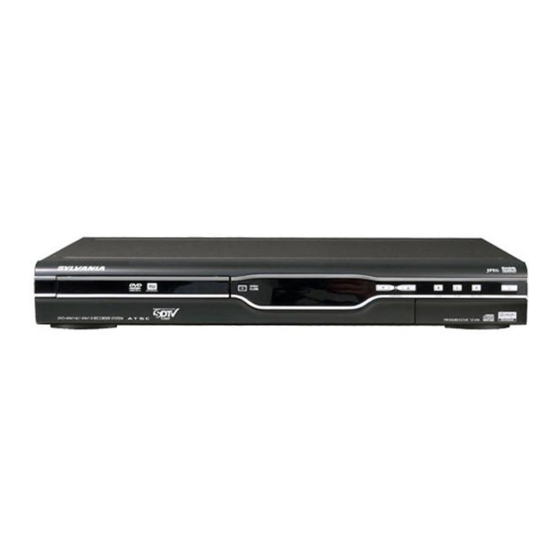
- Page 1 SERVICE MANUAL DVD RECORDER ZC350SL8...
-
Page 2: Table Of Contents
IMPORTANT SAFETY NOTICE Proper service and repair is important to the safe, reliable operation of all Funai Equipment. The service procedures recommended by Funai and described in this service manual are effective methods of performing service operations. Some of these service special tools should be used when and as recommended. -
Page 3: Specifications
SPECIFICATIONS Item Conditions Unit Nominal Limit 1. VIDEO 75 Ω load 1-1. Video Output Vp-p 1-2. S-Video Output 75 Ω load Y (Luminance) Vp-p 75 Ω load C (Chrominance) Vp-p 0.286 1-3. Component Output 75 Ω load Y (Luminance) Vp-p 75 Ω... -
Page 4: Laser Beam Safety Precautions
LASER BEAM SAFETY PRECAUTIONS This DVD player uses a pickup that emits a laser beam. Do not look directly at the laser beam coming from the pickup or allow it to strike against your skin. The laser beam is emitted from the location shown in the figure. When checking the laser diode, be sure to keep your eyes at least 30 cm away from the pickup lens when the diode is turned on. -
Page 5: Important Safety Precautions
IMPORTANT SAFETY PRECAUTIONS Product Safety Notice Also check areas surrounding repaired locations. J. Be careful that foreign objects (screws, solder Some electrical and mechanical parts have special droplets, etc.) do not remain inside the set. safety-related characteristics which are often not K. - Page 6 Safety Check after Servicing Examine the area surrounding the repaired location for damage or deterioration. Observe that screws, parts, and wires have been returned to their original positions. Afterwards, do the following tests and confirm the specified values to verify compliance with safety standards. 1.
-
Page 7: Standard Notes For Servicing
STANDARD NOTES FOR SERVICING Circuit Board Indications Pb (Lead) Free Solder 1. The output pin of the 3 pin Regulator ICs is When soldering, be sure to use the Pb free solder. indicated as shown. How to Remove / Install Flat Pack-IC Top View Bottom View 1. - Page 8 3. The flat pack-IC on the CBA is affixed with glue, so With Soldering Iron: be careful not to break or damage the foil of each 1. Using desoldering braid, remove the solder from pin or the solder lands under the IC when all pins of the flat pack-IC.
- Page 9 2. Installation With Iron Wire: 1. Using desoldering braid, remove the solder from 1. Using desoldering braid, remove the solder from all pins of the flat pack-IC. When you use solder the foil of each pin of the flat pack-IC on the CBA flux which is applied to all pins of the flat pack-IC, so you can install a replacement flat pack-IC more you can remove it easily.
- Page 10 Instructions for Handling Semi- conductors Electrostatic breakdown of the semi-conductors may occur due to a potential difference caused by electrostatic charge during unpacking or repair work. 1. Ground for Human Body Be sure to wear a grounding band (1 MΩ) that is properly grounded to remove any static electricity that may be charged on the body.
-
Page 11: Cabinet Disassembly Instructions
CABINET DISASSEMBLY INSTRUCTIONS 1. Disassembly Flowchart Note: (1) Identification (location) No. of parts in the figures This flowchart indicates the disassembly steps to gain (2) Name of the part access to item(s) to be serviced. When reassembling, (3) Figure Number for reference follow the steps in reverse order. - Page 12 (S-4) (S-4) [5] Power (L-1) Supply CBA CN1061 CN1060 (L-1) (L-1) [3] SW CBA (L-2) (L-3) (L-2) Fig. D4 [2] Front Assembly Fig. D2 (S-8) (S-2) M-PCB Plate Earth (S-3) [4] DVD (S-8) Mechanism (S-3) & DVD Main CN701 CBA Assembly [7] AV CBA (S-6) (S-7)
- Page 13 3. How to Eject Manually Note: When rotating the gear, be careful not to damage the gear. 1. Remove the Top Cover. 2. Rotate the gear in the direction of the arrow manually as shown below until the tray descends. 3.
-
Page 14: How To Initialize The Dvd Recorder
HOW TO INITIALIZE THE DVD RECORDER To put the program back at the factory-default, initialize the DVD recorder as the following procedure. 1. Turn the DVD recorder on. 2. Confirm that no disc is loaded or that the disc tray is open. -
Page 15: Firmware Renewal Mode
FIRMWARE RENEWAL MODE 1. Turn the power on and remove the disc on the tray. 4. Select the firmware version pressing arrow buttons, then press [ENTER]. 2. To put the DVD recorder into version up mode, Fig. d appears on the screen. The DVD recorder press [CM SKIP], [6], [5], and [4] buttons on the starts updating. -
Page 16: Function Indicator Symbols
FUNCTION INDICATOR SYMBOLS Note: If an error occurs, a message with the error number appears on the screen. Recording Error Error message You cannot record on this disc as Power Calibration Area is full. Error No. Error Message Solution Error Description Priority An error occurs during data reading. - Page 17 Error Message Solution Error Description Priority Disc is full. Insert the recordable disc with No avilable recording space. (No area for new recording) enough recording space. You cannot record on this disc as Power Calibration Area is Insert a new disc. PCA is Full.
-
Page 18: Block Diagrams
BLOCK DIAGRAMS System Control Block Diagram 1-9-1 E7H20BLS... - Page 19 Digital Signal Process Block Diagram 1-9-2 E7H20BLD...
- Page 20 Video Block Diagram REAR FRONT 1-9-3 E7H20BLV...
- Page 21 Audio Block Diagram 1-9-4 E7H20BLA...
- Page 22 Power Supply Block Diagram 1-9-5 E7H20BLP...
- Page 23 DTV Module Block Diagram 1-9-6 E7H20BLDTV...
- Page 24 SCHEMATIC DIAGRAMS / CBA’S Standard Notes WARNING Many electrical and mechanical parts in this chassis have special characteristics. These characteristics often pass unnoticed and the protection afforded by them cannot necessarily be obtained by using replacement components rated for higher voltage, wattage, etc.
- Page 25 LIST OF CAUTION, NOTES, AND SYMBOLS USED IN THE SCHEMATIC DIAGRAMS ON THE FOLLOWING PAGES: 1. CAUTION: FOR CONTINUED PROTECTION AGAINST FIRE HAZARD, REPLACE ONLY WITH THE SAME TYPE FUSE. ATTENTION: POUR UNE PROTECTION CONTINUE LES RISQES D'INCELE N'UTILISER QUE DES FUSIBLE DE MÊME TYPE. RISK OF FIRE-REPLACE FUSE AS MARKED.
- Page 26 AV 1/5 Schematic Diagram * NOTE These components (IC1502, C1509) can be used in any models. However, you cannot mix components under Group A with the ones under Group B. You can choose either Group. The difference between Group A and Group B is shown below. Group A Group B R3112N191A-TR-FA...
- Page 27 AV 2/5 Schematic Diagram 1-10-4 E7H20SCAV2...
- Page 28 AV 3/5 Schematic Diagram 1-10-5 E7H20SCAV3...
- Page 29 AV 4/5 Schematic Diagram E7H20SCAV4 1-10-6...
- Page 30 AV 5/5 Schematic Diagram FL2001 MATRIX CHART BS CS DR DTV BS CS E7H20SCAV5 1-10-7...
- Page 31 Power Supply Schematic Diagram CAUTION ! For continued protection against fire hazard, CAUTION ! replace only with the same type fuse. Fixed voltage (or Auto voltage selectable) power supply circuit is used in this unit. NOTE: ATTENTION : Pour une protection continue les risqes The voltage for parts in hot circuit is measured using If Main Fuse (F1001) is blown , check to see that all components in the power supply d'Incele n'utiliser que des fusible de même type.
- Page 32 SW Schematic Diagram 1-10-9 E7H20SCSW...
- Page 33 DVD Main 1/5 Schematic Diagram 1 NOTE: The order of pins shown in this diagram is different from that of actual IC101. IC101 is divided into five and shown as IC101 (1/5) ~ IC101 (5/5) in this DVD Main Schematic Diagram Section. 1-10-10 E7H20SCD1...
- Page 34 DVD Main 2/5 Schematic Diagram 1 NOTE: The order of pins shown in this diagram is different from that of actual IC101. IC101 is divided into five and shown as IC101 (1/5) ~ IC101 (5/5) in this DVD Main Schematic Diagram Section. 1-10-11 E7H20SCD2...
- Page 35 DVD Main 3/5 Schematic Diagram 1 NOTE: The order of pins shown in this diagram is different from that of actual IC101. IC101 is divided into five and shown as IC101 (1/5) ~ IC101 (5/5) in this DVD Main Schematic Diagram Section. E7H20SCD3 1-10-12...
- Page 36 DVD Main 4/5 Schematic Diagram 1 NOTE: The order of pins shown in this diagram is different from that of actual IC101. IC101 is divided into five and shown as IC101 (1/5) ~ IC101 (5/5) in this DVD Main Schematic Diagram Section. 1-10-13 E7H20SCD4...
- Page 37 DVD Main 5/5 Schematic Diagram 1 NOTE: The order of pins shown in this diagram is different from that of actual IC101. IC101 is divided into five and shown as IC101 (1/5) ~ IC101 (5/5) in this DVD Main Schematic Diagram Section. E7H20SCD5 1-10-14...
- Page 38 DTV Module 1/2 Schematic Diagram 1-10-15 E7H20SCDTV1...
- Page 39 DTV Module 2/2 Schematic Diagram E7H20SCDTV2 1-10-16...
- Page 40 AV CBA Top View BE7H50F01013A 1-10-17...
- Page 41 AV CBA Bottom View C1418 PLUS LEAD PIN 3 OF CN1101 PIN 5 OF CN1101 PIN 7 OF CN1101 PIN 9 OF CN1101 PIN 17 OF CN1101 PIN 3 OF CN1051 BE7H50F01013A 1-10-18...
- Page 42 Power Supply CBA Top View CAUTION ! Because a hot chassis ground is present in the power CAUTION ! supply circut, an isolation transformer must be used. Fixed voltage (or Auto voltage selectable) power supply circuit is used in this unit. For continued protection against fire hazard, If Main Fuse (F1001) is blown , check to see that all components in the power supply Also, in order to have the ability to increase the input...
- Page 43 Power Supply CBA Bottom View CAUTION ! Because a hot chassis ground is present in the power CAUTION ! supply circut, an isolation transformer must be used. Fixed voltage (or Auto voltage selectable) power supply circuit is used in this unit. For continued protection against fire hazard, If Main Fuse (F1001) is blown , check to see that all components in the power supply Also, in order to have the ability to increase the input...
- Page 44 SW CBA Top View SW CBA Bottom View BE7H50F01013C 1-10-21...
-
Page 45: Waveforms
WAVEFORMS Pin 7 of CN1101 Pin 5 of CN1101 VIDEO-Y 0.2V 20µsec VIDEO-Cr 0.2V 20µsec Pin 9 of CN1101 Pin 17 of CN1101 VIDEO-C 0.2V 20µsec AUDIO(L)-OUT 0.5ms C1418 PLUS LEAD Pin 3 of CN1051 VIDEO-CVBS 0.5V 20µsec SPDIF 0.1µsec Pin 3 of CN1101 NOTE: Input: COLOR BAR SIGNAL... -
Page 46: Wiring Diagram
WIRING DIAGRAM SUB-RXD SUB-TXD SYS-RESET FCS(+) FOCUS SUB-SCLK FCS(-) ACTUATOR TRK(+) TRACKING TRK(-) ACTUATOR TILT(+) TILT VIDEO-C-IN TILT(-) ACTUATOR LDD-IIN4 VIDEO-Y/CVBS-IN 20 LDD-IIN3 AUDIO+5V LDD-IIN2 DVD-AUDIO-MUTE 18 LDD-IINR AUDIO(L)-OUT 17 LDD-VDD DVD-LD AUDIO(R)-OUT 15 LDD-VDD LDD-ENABLE AUDIO(R)-IN 13 LDD-OSCEN CD-LD AUDIO(L)-IN LDD-WEN4 VIDEO-C-OUT 9... -
Page 47: System Control Timing Charts
SYSTEM CONTROL TIMING CHARTS [ Tray Open ] Push Close Power on button is pressed. Tray insertion INNER-SW open? Tray insertion INNER-SW open? Tray ejection To disc distinction [ Tray Open ] button is pressed. INNER-SW open? SLED moves Tray ejection 1-13-1 R4NTI... - Page 48 Parameter V*: Voltage T*: Event timer V0: 2.40 V T1: 0.050 s V1: 4.25 V T2: 2.000 s V2: 2.00 V T3: 0.008 s V3: 2.36 V T4: 0.006 s V4: 4.26 V T5: 0.066 s T6: 1.500 s T7: 0.800 s T8: 0.005 s Tray open Tray ejection direction...
- Page 49 Push close Threshold level 0.08 V 0.02 s Push Close detection 1-13-3 R4NTI...
-
Page 50: Ic Pin Function Descriptions
IC PIN FUNCTION DESCRIPTIONS IC1501 (SUB MICRO CONTROLLER) Signal Function Name Signal Function Name Serial Data IN KEY-1 Key Data Input 1 34 OUT SCL Serial Clock IN KEY-2 Key Data Input 2 FLASH- Serial Data Signal for Flash IN POW-SW Abnormal Voltage Detection IN AFT Tuner Voltage Input Signal... - Page 51 IC2001 (VFD DRIVER) Signal Function Name IN CLK Serial Clock IN STB Serial Interface Strobe Not Used Not Used Power Supply Segment Output Pull Down Level 16 OUT i Segment Output Grid Output Power Supply IN OSC Oscillator Input Not Used IN DIN Serial Data Input 1-14-2...
-
Page 52: Lead Identifications
LEAD IDENTIFICATIONS KRC103M-AT/P KTA1271-Y-AT/P RN1402 KIA4558P/P KTA1267-GR-AT/P KTC3205-Y-AT/P KRC102S-RTK/P KTC3199-GR-AT/P E C B E C B MM1697AJBE PQ070XF01SZH 2SK3563(Q) KTB1151-Y-U/P SC16313G 1 2 3 4 G D S E C B AN5832SA-E1V CD4052BNSR BU4219G-TR MN101C77AFP1 MM1637XVBE R3112N191A-TR-FA R3112N191A-TR-FB PST3619NR 1 2 3 Note: PS2561A-1(W) UTC4580E... -
Page 53: Exploded Views
EXPLODED VIEWS Cabinet See Electrical Parts List 2L010 for parts with this mark. Some Ref. Numbers are not in sequence. 2L010 2L030 2L041 2B49 AC1001 2L050 POWER SUPPLY CBA 2L010 2B10 2L040 DVD Mechanism & DVD Main CBA Assembly AV CBA DTV MODULE CBA UNIT 2L011 2L044... - Page 54 Packing Upper Side Lower Side Unit Some Ref. Numbers are not in sequence. 1-16-2 E7H20PEX...
-
Page 55: Mechanical Parts List
REAR PANEL E7H20UID 1VM222966 FOOT H5100UD 0VM406940A MODEL NO LABEL E7H20UD ---------- LABEL BAR CODE HB400UD ---------- LABEL TELEPHONE NUMBER ---------- H5730UD(SYLVANIA) PCB CUSHION E7C40UD 1VM425421A 2B10 PCB SUPPORT/PCB SPACERS KGLS-14S XP0U027WD001 2B11 FRONT BRACKET R E2A00JD 1VM424123F 2B15 MAIN PCB HOLDER E2B10ED... -
Page 56: Electrical Parts List
ELECTRICAL PARTS LIST PRODUCT SAFETY NOTE: Products marked with a Ref. No. Description Part No. # have special characteristics important to safety. C1135 ELECTROLYTIC CAP . 220µF/16V M CE1CMASDL221 Before replacing any of these components, read C1152 ELECTROLYTIC CAP . 100µF/16V M CE1CMASDL101 carefully the product safety notice in this service C1171... - Page 57 Ref. No. Description Part No. Ref. No. Description Part No. If C1509 is 0.015µF, then IC1502 is R3112N191A-TR-FA, R3112N191A-TR-FB or C2008 ELECTROLYTIC CAP . 3.3µF/50V M CE1JMASDL3R3 BU4219G-TR. C2009 ELECTROLYTIC CAP . 3.3µF/50V M CE1JMASDL3R3 C1509 CHIP CERAMIC CAP .(1608) B K 0.015µF/50V CHD1JK30B153 C2010 ELECTROLYTIC CAP .
- Page 58 Ref. No. Description Part No. Ref. No. Description Part No. CHIP RES.(1608) 1/10W 0 Ω CHIP RES.(1608) 1/10W F 33k Ω L1761 RRXAZR5Z0000 R1121 RRXAFR5H0333 CHIP RES.(1608) 1/10W 0 Ω CHIP RES.(1608) 1/10W F 33k Ω L1762 RRXAZR5Z0000 R1122 RRXAFR5H0333 CHIP RES.(1608) 1/10W 0 Ω...
- Page 59 Ref. No. Description Part No. Ref. No. Description Part No. CHIP RES. 1/10W J 820k Ω CHIP RES. 1/10W J 33 Ω R1505 RRXAJR5Z0824 R2001 RRXAJR5Z0330 CHIP RES. 1/10W J 47k Ω CHIP RES. 1/10W J 68k Ω R1506 RRXAJR5Z0473 R2003 RRXAJR5Z0683 CHIP RES.
- Page 60 Ref. No. Description Part No. Ref. No. Description Part No. CARBON RES. 1/4W J 100k Ω C1066 CERAMIC CAP . B K 220pF/500V CCD2JKS0B221 R1014 RCX4JATZ0104 CARBON RES. 1/4W J 470k Ω C1067 ELECTROLYTIC CAP . 10µF/50V M CE1JMASDL100 R1015 RCX4JATZ0474 CARBON RES.
- Page 61 Misuse of any trademarks or any other content in this manual is strictly prohibited. Funai shall aggressively enforce its intellectual property rights to the fullest extent of the law. ZC350SL8 E7H20UD 2007-3-28...