
Related Manuals for Panasonic SA-VK72DGCS


Summary of Contents for Panasonic SA-VK72DGCS
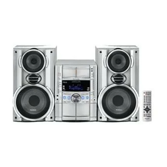
- Page 1 ORDER NO. MD0506272C3 DVD Stereo System SA-VK72DGCS / SA-VK72DGS Colour (S)... Silver Type SPECIFICATIONS Specifications PDF created with pdfFactory Pro trial version www.pdffactory.com...
- Page 2 AMPLIFIER SECTION RMS Output Power: Dolby Digital Mode Main 70 W per channel (6 ), 1 kHz, 10% THD Surround Ch 55 W per channel (6 ), 1 kHz, 10% THD Center Ch 70 W per channel (6 ), 1 kHz, 10% THD Total RMS Dolby Digital mode power 320 W PMPO output power...
- Page 3 (1) DVD (DVD-Video, DVD-Audio) (2) DVD-RAM (DVD-VR, JPEG* 4,*5) (3) DVD-R (DVD-Video) (4) DVD-RW (DVD-Video) + R/RW (Video) (5) CD,CD-R/RW [CD-DA, Video CD, SVCD* 1, MP3* 2,* 5, WMA* 3, * 5, JPEG* 4,* 5, HighMAT Level 2 (Audio and Image)] * 1 Conforming to IEC62107 * 2 MPEG-1 Layer 3, MPEG-2 Layer 3 * 3 Windows Media Audio Ver.9.0.
- Page 4 Mass 8.8 kg Operating temperature range +5°C to +35°C Operating humidity range 5% to 90% RH (no condensation) SYSTEM SC-VK72D (GCS) Music System: SA-VK72D (GCS) Front Speakers: SB-VK72 (GC) Satelite Speakers: SB-PT72 (GC) SC-VK72D (GS) Music System: SA-VK72D (GS) Front Speakers: SB-VK72 (GC) Satelite Speakers: SB-PT72 (GC) Notes: 1.
- Page 5 1. Safety precautions for AC Cord (For GS only) 2. Before Use (Caution) Be sure to disconnect the AC cord before adjusting the voltage selector. Use a minus(-) screwdriver to set the voltage selector (on the rear panel) to the voltage setting for the area in which the unit will be used.
- Page 6 - No sound is heard when the power is turned on. - Sound stops during a performance. The function of this circuitry is to prevent circuitry damage if, for example, the positive and negative speaker connection wires are “shorted”, or if speaker systems with an impedance less than the indicated rated impedance of the amplifier are used.
- Page 7 5.1.2. Leakage Current Hot Check / (See Figure 1) 1. Plug the AC cord directly into the AC outlet. Do not use an isolation transformer for this check. 2. Connect a 1.5k , 10 watts resistor, in parallel with a 0.15 capacitor, between each exposed metallic part on the set and a good earth ground such as a water pipe, as shown in Figure 1.
- Page 8 1. Immediately before handling any semiconductor component or semiconductor-equipped assembly, drain off any ESD on your body by touching a known earth ground. Alternatively, obtain and wear a commercially available discharging ESD wrist strap, which should be removed for potential shock reasons prior to applying power to the unit under test.
- Page 9 7. Handling the Lead-free Solder 7.1. About lead free solder (PbF) Distinction of PbF P.C.B.: P.C.B.s (manufactured) using lead free solder will have a PbF stamp on the P.C.B. Caution: - Pb free solder has a higher melting point than standard solder; Typically the melting point is 50 - 70°F (30 - 40°C) higher.
- Page 10 CAUTION! THIS PRODUCT UTILIZES A LASER. USE OF CONTROLS OR ADJUSTMENTS OR PERFORMANCE OF PROCEDURES OTHER THAN THOSE SPECIFIED HEREIN MAY RESULT IN HAZARDOUS RADIATION EXPOSURE. Use of Caution Labels PDF created with pdfFactory Pro trial version www.pdffactory.com...
- Page 11 PDF created with pdfFactory Pro trial version www.pdffactory.com...
- Page 12 9. Cautions to be taken when handling Optical Pickup The laser diode used inside optical pickup could be destroyed due to static electricity as a potential difference is caused by electrostatic load discharged from clothes or human body. Handling the parts carefully to avoid electrostatic destruction during repair. 9.1.
- Page 13 and be sure to check that the short land is open, before connecting. (Please remove solder, when the short land short-circuits.) 9.3. Grounding for Preventing Electrostatic Destruction 1. Human body grounding Use the anti-static wrist strap to discharge the static electricity accumulated in your body.
- Page 14 AC cord AC cord (For GS only) FM antenna AM antenna Video cable PDF created with pdfFactory Pro trial version www.pdffactory.com...
- Page 15 11. Operation Procedures 12. Disc information 13. About HighMAT 13.1. What’s HighMAT? Consumers worldwide are using PCs to create their own collections of music, photos and even video by burning them onto CDs. But how these collections can be experienced across different devices can be confusing to navigate, time consuming to access for a DVD player, and be incomplete in terms of music information available to the customer.
- Page 16 13.2. Why take advantage of HighMAT? A Problem Defined:Today, when consumers create their own digital audio, video or photo collections on CD-R or other physical formats, there are numerous, inconsistent ways that devices read the data. For the consumer, the playback experience can be confusing: A Solution Created: HighMAT delivers a better digital media access experience by creating a standard approach for PCs to structure digital media on various physical formats and for playback devices to read the data.
- Page 17 Conventional HighMAT Even though DVD player is CD-R/RW compatible, the HighMAT compatible products play content inconsistent ways that various DVD players can read with consistent interface. This includes products the music or photos files often leads to a confusing which are JPEG compatible products without and inconsistant playback experince.
- Page 18 PDF created with pdfFactory Pro trial version www.pdffactory.com...
- Page 19 HighMAT is now available for CD Burning and in Leading DVD PlayersHighMAT is a new technology that is now available in leading software and consumer electronic devices to dramatically improve the digital media experience when you create homemade CDsHighMAT delivers a simple, standardized way for PC software and consumer electronics devices to talk to each other and work better together.
- Page 20 This unit is equipped with the optical pickup self-diagnosis function and the tilt adjustment check function. Follow the procedure described below during repair in order to perform self- diagnosis and tilt adjustment effectively. Especially when “NO DISC” is displayed, be sure to apply the self-diagnosis function before replacing with an optical pickup.
- Page 21 15.2. Automatic Displayed Error Codes 15.2.1. Automatic Display Function For a power unit error, the code is automatically displayed. F61: Automatically displayed on the LCD of the player. 15.2.2. Re-Display - For F61 Display - When the code, F61 is displayed, the power is automatically turned off.
- Page 22 15.2.3. Description of Error Code 15.2.3.1. F61 - State, Condition When the power is turned on, the unit is automatically turned off. The power does not turn on. - Cause, Troubleshooting Power circuit system failure and/or direct current flown to speaker terminal / Identify the cause and replace with new parts.
- Page 23 Player Remote Usage Controller Unit Error code display (Refer to the Item 15.5. DVD/CD Self-Diagnosis Code Description) button Tilt adjustment (Jitter) Region number and broadcasting system check Bulit-in program version check (Micro-P) FUNCTIONS DVD laser drive current check CD laser drive current check PAUSE Writing of laser drive current value after replacement of optical (Do use this function only when optical pickup is replaced.)
- Page 24 Error Code Meaning Details F103 IIlegal highlight position Disc standard is possibly illegal when highlight is displayed. IIC Error F4FF Forced initialization failure (Time out) F880 Unsuitable task number When a message arrives from not existing F890 A message is sent during AV task During transmission of a message to AV transmission F891...
- Page 25 Item Operational Details Display Condition and Key Function Error code While the player Error code display / DVD_F--- / *nn: Error Press display is stopped and no Displays the latest error history / *--: Error number STOP disc is inserted, code stored in EEPROM.
- Page 26 Item Operational Details Display Condition and Key Function Measurement of While the player Measurement of DVD laser /xxx yyyy Automatically DVD laser is stopped and no current electricity / (display1/display2) / / exits current disc is inserted, Measures DVD laser current DVD laser current mode electricity...
- Page 27 Item Operational Details Display Condition and Key Function Measurement of While the player Measurement of CD laser /xxx yyyy Automatically CD laser is stopped and no current electricity / (display1/display2) / / exits current disc is inserted, Measures CD laser current CD laser current mode electricity...
- Page 28 Item Operational Details Display Condition and Key Function Firmware While the player Firmware version display Automatically version display is stopped and no Panel computer release exits disc is inserted, number / : System mode press and hold computer generation / five System computer model down the...
- Page 29 Item Operational Details Display Condition and Key Function Reset laser use While the usage Laser usage time reset / T1_ _0000/0000 (display1/ Automatically time time 1 is Resets both for DVD and CD display2) exits displayed, press at once. mode and hold down the five button on...
- Page 30 Item Operational Details Display Condition and Key Function Communication While the player Displays frequency of ECC_ _ _ 00 Press error display / is stopped and no communication errors STOP disc is inserted, between system computer Open press and hold firm IC and mechanical on the computer IC during DVD...
- Page 31 [POWER] KEY on the remote control for 3 seconds to enter Lock mode B. [_LOCKED_] will be displayed for 3 seconds, and the current disc will begin playing. 2. Lock mode B primarily controls the selector and disc operations, and disenables for the following keys. Note: OPEN/CLOSE button are invalid and the player displays “_LOCKED_”...
- Page 32 Note: It is prohibited to unplug the power cable while the tray is opened and to close the tray manually. 16. Cautions To Be Taken During Servicing 16.1. Recovery after the dvd player is repaired - When Flash ROM or DVD Module P.C.B. is replaced, carry out the recovery processing to optimize the drive.
- Page 33 2. The recovery process automatically starts, and a message of completion prompts on the screen. 3. Remove the disc. 4. Turn off the power. 16.4.2. Version Upgrade Process 1. Insert the recovery disc to the player to replay. 2. The version of player is automatically checked and prompts if necessary.
- Page 34 controller unit. / Spindle motor usage time: press both the button on the player and the button on the remote controller unit. 2. Purpose of Use To obtain reference data of laser and spindle motor systems during failure diagnosis. / To check faulty parts during re-repair. 16.6.
- Page 35 - Disassembly of Top Cabinet - Disassembly of Rear Panel - Disassembly of DVD Changer Unit - Disassembly of Main P.C.B. - Disassembly of Power Amp P.C.B. - Disassembly of Power P.C.B. - Disassembly of Transformer P.C.B. & Voltage Selector - Disassembly of Front Panel Unit - Disassembly of Mic P.C.B.
- Page 36 17.4. Disassembly of Rear Panel - Follow the (Step 1) - (Step 2) of Item 17.3 - Disassembly of Top Cabinet Step 1 Remove 12 screws and disconnect cables CN2810 and CN2813 (Fan) at rear panel as shown. 17.5. Disassembly of DVD Changer Unit - Follow the (Step 1) - (Step 2) of Item 17.3 - Disassembly of Top Cabinet Step 1 Remove 1 screw at rear panel.
- Page 37 Step 2 Detach the FFC cables (CN2810 & CN2813). Step 3 Release the claws on both ends, and remove the DVD changer unit. PDF created with pdfFactory Pro trial version www.pdffactory.com...
- Page 38 Step 4 Lift the DVD changer unit upwards. Step 5 Remove 2 screws. Step 6 Remove the DVD chassis. Step 7 Lay the unit. PDF created with pdfFactory Pro trial version www.pdffactory.com...
- Page 39 - For disassembly of DVD mechanism unit, please refer to Section 17.16 of this manual. 17.6. Disassembly of Main P.C.B. - Follow the (Step 1) - (Step 2) of Item 17.3 - Disassembly of Top Cabinet - Follow the (Step 1) of Item 17.4 - Disassembly of Rear Panel - Follow the (Step 1) - (Step 4) of Item 17.5 - Disassembly of DVD Changer Unit Step 1 Disconnect FFC cables (CP6803, CN2811, CN2808 and CN2814).
- Page 40 Changer Unit - Follow the (Step 1) - (Step 2) of Item 17.6 - Disassembly of Main P.C.B. Step 1 Remove the 2 screws at Power Amp P.C.B.. Step 2 Remove the 2 screws at each Power Amp IC. Step 3 Lift up the Power Amp P.C.B. to remove it. PDF created with pdfFactory Pro trial version www.pdffactory.com...
- Page 41 Step 4 Desolder wire at holder H5804. - Replacement of the Power Amp IC Repeat Step 1 - Step 3 of Section 17.7 - Disassembly of Power Amp P.C.B. 17.8. Disassembly of Power P.C.B. - Follow the (Step 1) - (Step 2) of Item 17.3 - Disassembly of Top Cabinet - Follow the (Step 1) of Item 17.4 - Disassembly of Rear Panel - Follow the (Step 1) - (Step 4) of Item 17.5 - Disassembly of DVD...
- Page 42 Note: Insulate the Power P.C.B. with insulation material to avoid short circuit. - Replacement of the Power Amp IC or Voltage Regulator Step 1 Remove 2 screws at the Power Amp IC and or 1 screw to Voltage Regulator. PDF created with pdfFactory Pro trial version www.pdffactory.com...
- Page 43 Step 2 Break the joints with a metal cutter as shown below. Step 3 Unsolder the terminals to replace the components. Step 4 Fix back the cut portion with a screw as shown. PDF created with pdfFactory Pro trial version www.pdffactory.com...
- Page 44 17.9. Disassembly of Transformer P.C.B. & Voltage Selector - Follow the (Step 1) - (Step 2) of Item 17.3 - Disassembly of Top Cabinet - Follow the (Step 1) of Item 17.4 - Disassembly of Rear Panel - Follow the (Step 1) - (Step 4) of Item 17.5 - Disassembly of DVD Changer Unit - Follow the (Step 1) - (Step 2) of Item 17.6 - Disassembly of Main P.C.B.
- Page 45 Step 2 Bent the front panel unit forward as arrow shown. Step 3 Press the 2 catch holders on both sides of the front panel unit to release the claws. Step 4 Remove the front panel unit. Note: Ensure 2 claws on bottom chassis is properly and fully catched to the front panel holes. 17.11.
- Page 46 Cabinet - Follow the (Step 1) - (Step 4) of Item 17.5 - Disassembly of DVD Changer Unit - Follow the (Step 1) - (Step 4) of Item 17.10 - Disassembly of Front Panel Unit Step 1 Remove volume knob. Step 2 Remove 2 screws.
- Page 47 Step 4 Remove 10 screws. Step 5 Disconnect FFC cable at CP6800. Step 6 Release 2 catches. 17.11.1. Disassembly of Lid Step 1 Lift the spring sideward. Step 2 Remove Lid. Note: Do not misplace the spring. 17.12. Disassembly of Deck Mechanism Unit - Follow the (Step 1) - (Step 2) of Item 17.3 - Disassembly of Top Cabinet - Follow the (Step 1) - (Step 6) of Item 17.5 - Disassembly of DVD...
- Page 48 - Follow the (Step 1) - (Step 4) of Item 17.10 - Disassembly of Front Panel Unit Step 1 Detach FFC wire CN971. Step 2 Disconnect FFC flat cable from the connector CN1001. Step 3 Remove the 5 screws. Step 4 Push the lever upward, and then open the cassette lid ass’y (For DECK1 and DECK2). Step 5 Tilt the cassette mechanism unit in the direction of arrow (1), and then remove it in the direction of arrow (2).
- Page 49 Changer Unit - Follow the (Step 1) - (Step 4) of Item 17.10 - Disassembly of Front Panel Unit - Follow the (Step 1) - (Step 5) of Item 17.12 - Disassembly of Deck Mechanism Unit Step 1 Remove 2 screws. Step 2 Unsolder the motor terminals.
- Page 50 Step 2 Remove DVD traverse deck by rotating to the arrow direction. 17.15. Replacement for Optical Pickup Unit (DVD mechanism) - Follow the (Step 1) - (Step 2) of Item 17.3 - Disassembly of Top Cabinet - Follow the (Step 1) - (Step 7) of Item 17.5 - Disassembly of DVD Changer Unit - Follow the (Step 1) - (Step 2) of Item 17.14 - Replacement of PDF created with pdfFactory Pro trial version...
- Page 51 Traverse Deck Step 1 Pull out FFC. Step 2 Widening the catch, push the pin in. Step 3 Remove 4 pins. PDF created with pdfFactory Pro trial version www.pdffactory.com...
- Page 52 Step 4 Remove the traverse deck. Note: As floating springs (4 pieces) come off at the same time, be careful not to lose them. Step 6 Remove the dvd module board and turn it over. Step 7 Pull FFC out from the connector. Note: Insert a short pin into FFC of the optical pickup.
- Page 53 Step 8 Rotate the traverse deck (B) to the arrow direction and shift the optical pickup to the furthest backward. Step 9 Remove 1 screw. Step 10 Remove the catch of the drive rack, and take out the drive rack. PDF created with pdfFactory Pro trial version www.pdffactory.com...
- Page 54 Step 11 Place the convex part of an optical pickup to the concave part of a traverse base, then take out the optical pickup. 17.16. Procedure for removing CD loading mechanism 1. Turn off by pressing power SW in the body. PDF created with pdfFactory Pro trial version www.pdffactory.com...
- Page 55 2. Unplug AC power cord after the indication of [GOOD-BYE], then disassemble the body. 3. Disassemble the body, and take out CD loading mechanism. 4. Perform disassembly according to the following procedure for disassembly. 17.17. CR16 mechanism disassembly procedure 17.17.1. Gear for servicing information - This unit has a gear which used for checking items (open/close of disc tray, up/down operation of traverse unit by manually) when servicing.
- Page 56 PDF created with pdfFactory Pro trial version www.pdffactory.com...
- Page 57 PDF created with pdfFactory Pro trial version www.pdffactory.com...
- Page 58 PDF created with pdfFactory Pro trial version www.pdffactory.com...
- Page 59 17.17.3. Replacement for the traverse deck - Follow the (Step 1) - (Step 10) of item 17.17.2. PDF created with pdfFactory Pro trial version www.pdffactory.com...
- Page 60 PDF created with pdfFactory Pro trial version www.pdffactory.com...
- Page 61 17.17.4. Disassembly for CD loading unit - Follow the (Step 1) - (Step 10) of item 17.17.2. - Follow the (Step 1) - (Step 4) of item 17.17.3. PDF created with pdfFactory Pro trial version www.pdffactory.com...
- Page 62 PDF created with pdfFactory Pro trial version www.pdffactory.com...
- Page 63 PDF created with pdfFactory Pro trial version www.pdffactory.com...
- Page 64 PDF created with pdfFactory Pro trial version www.pdffactory.com...
- Page 65 PDF created with pdfFactory Pro trial version www.pdffactory.com...
- Page 66 PDF created with pdfFactory Pro trial version www.pdffactory.com...
- Page 67 17.18. CR16 mechanism assembly procedure The following specified greases and/or oil must be applied when some specific parts are changed. 1. Floil grease (VFK1298) : The floil grease must be applied to tray, tray (L) and tray (R). 2. Hanarl oil (VFK1700) : The hanarl oil must be applied to any parts with grease other than the said parts.
- Page 68 PDF created with pdfFactory Pro trial version www.pdffactory.com...
- Page 69 PDF created with pdfFactory Pro trial version www.pdffactory.com...
- Page 70 PDF created with pdfFactory Pro trial version www.pdffactory.com...
- Page 71 PDF created with pdfFactory Pro trial version www.pdffactory.com...
- Page 72 PDF created with pdfFactory Pro trial version www.pdffactory.com...
- Page 73 PDF created with pdfFactory Pro trial version www.pdffactory.com...
- Page 74 PDF created with pdfFactory Pro trial version www.pdffactory.com...
- Page 75 PDF created with pdfFactory Pro trial version www.pdffactory.com...
- Page 76 PDF created with pdfFactory Pro trial version www.pdffactory.com...
- Page 77 PDF created with pdfFactory Pro trial version www.pdffactory.com...
- Page 78 PDF created with pdfFactory Pro trial version www.pdffactory.com...
- Page 79 PDF created with pdfFactory Pro trial version www.pdffactory.com...
- Page 80 PDF created with pdfFactory Pro trial version www.pdffactory.com...
- Page 81 PDF created with pdfFactory Pro trial version www.pdffactory.com...
- Page 82 PDF created with pdfFactory Pro trial version www.pdffactory.com...
- Page 83 PDF created with pdfFactory Pro trial version www.pdffactory.com...
- Page 84 PDF created with pdfFactory Pro trial version www.pdffactory.com...
- Page 85 PDF created with pdfFactory Pro trial version www.pdffactory.com...
- Page 86 PDF created with pdfFactory Pro trial version www.pdffactory.com...
- Page 87 PDF created with pdfFactory Pro trial version www.pdffactory.com...
- Page 88 PDF created with pdfFactory Pro trial version www.pdffactory.com...
- Page 89 PDF created with pdfFactory Pro trial version www.pdffactory.com...
- Page 90 17.19. Disassembly for Traverse Unit - Follow the (Step 1) - (Step 10) of item 17.17.2 - Follow the (Step 1) - (Step 4) of item 17.17.3 PDF created with pdfFactory Pro trial version www.pdffactory.com...
- Page 91 PDF created with pdfFactory Pro trial version www.pdffactory.com...
- Page 92 17.20. Replacement for cassette lid - Follow the (Step 1) - (Step 2) of Item 17.3 - Disassembly of Top Cabinet Step 1 Lift up the lever upward, open the cassette deck. (For DECK1 and DECK2) PDF created with pdfFactory Pro trial version www.pdffactory.com...
- Page 93 Step 2 Push up the cassette lid (L/R) in the direction of arrow. (For DECK1 and DECK2). 17.21. Rectification for tape jam problem - Follow the (Step 1) - (Step 2) of Item 17.3 - Disassembly of Top Cabinet Step 1 If a cassette tape cannot be removed from the deck (the tape is caught by the capstan or pinch roller during playback or recording), rotate the flywheel F in the direction of the arrow to remove it.
- Page 94 Step 2 Push the lever upward and open the cassette lid. Remove the cassette tape. 18. Checking for major P.C.Bs Note: Checking of all major P.C.Bs (Main P.C.B., Panel P.C.B., Transformer P.C.B., Deck P.C.B., Deck PDF created with pdfFactory Pro trial version www.pdffactory.com...
- Page 95 Mechanism P.C.B., Mic P.C.B., Power P.C.B. and Power Amp P.C.B.) can be carried out using below procedures. For the disassembling procedures, refer to Section 17. 18.1. Checking of Main P.C.B. 1. Remove Top Cabinet. 2. Disassemble DVD Changer Unit. 3. Connect FFC cables (CN2810 & CN2813) from Main P.C.B. 18.2.
- Page 96 3. Connect FFC cables (CN2810 & CN2813) from Main P.C.B. 18.3. Checking of Panel, Deck & Deck Mechanism P.C.B. 1. Remove Top Cabinet. 2. Disassemble DVD Changer Unit. 3. Disassemble Front Panel Unit. 4. Remove volume knob and Mic Jack Holder. 5.
- Page 97 7. Use the extension cable (A) to reconnect (CN1001) Deck P .C.B. and (CP6803) Main P.C.B. 8. Use the extension cable (B) to reconnect (CP6800) Panel P.C.B. and (CN971) Deck Mechanism P.C.B. Service Tools Extension FFC (A) Deck P.C.B. - Main P.C.B. REEX0485 (14 Pins) (B) Panel P.C.B.
- Page 98 3. Remove 4 screws at Transformer P.C.B.. 4. Remove 2 screws at heat sink and 1 screw at Power P.C.B. 5. Flip the Power P.C.B. 6. Insulate the Power P.C.B. with insulation material to avoid short circuit. 7. Use the extension cable (A) to reconnect (CN1001) Deck P.C.B. and (CP6803) Main P.C.B.
- Page 99 - Judgeable room temperature 20 ± 5 °C (68 ± 9°F) - Measuring instrument - EVM (DC Electronic voltmeter) - Digital frequency counter - Test Tape - Tape speed gain adjustment (3 kHz, -10 dB); QZZCWAT 19.1.1. Head Azimuth Adjustment (Deck 1/2) Caution: - Please replace both azimuth adjustment screw and springs simultaneously when readjusting the head azimuth.
- Page 100 19.1.2. Tape Speed Adjustment (Deck 1/2) 1. Set the tape edit button to “NORMAL” position. 2. Insert the test tape (QZZCWAT) to DECK 2 and playback (FWD side) the middle portion of it. 3. Adjust Motor VR (DECK 2) for the output value shown below. Adjustment target: 2940 ~ 3060 Hz (NORMAL speed) 4.
- Page 101 value. Bias voltage for Deck 2 14±4mV (Normal) Fig. 2 Fig. 3 19.1.4. Bias Frequency Adjustment (Deck 1/2) 1. Set the unit to “AUX” position. 2. Insert the Normal blank tape (QZZCRA) into DECK 2 and set the unit to “REC” mode ( use “REC/STOP”...
- Page 102 4. Adjust Z2602 so that the output frequency is maximized in Fig. 6. Fig. 5 Fig. 6 19.2.2. AM RF Adjustment 1. Connect the instrument as shown in Fig. 7. 2. Set the unit to AM mode. 3. Set AM-SG to 520kHz. 4.
- Page 103 19.3. Alignment Points 19.3.1. Cassette Deck Section 19.3.2. Adjustment Point 20. Block Diagram PDF created with pdfFactory Pro trial version www.pdffactory.com...
- Page 104 21. Voltage Measurement This section is not available at time of issue. 22. Schematic Diagram (All schematic diagrams may be modified at any time with the development of the new technology) Note: : Stock Switch : Play Switch : Bottom Switch : Open Switch : Change Switch S951...
- Page 105 S6801 : Tape Switch S6802 : Tuner/Band Switch S6803 : AUX Switch S6804 : Deck 1 Switch S6805 : Display/Demo Switch S6806 : Deck 2 Switch S6807 : Rew Switch S6808 : FF Switch S6809 : Stop Switch S6810 : AC In Switch S6811 : Disc Check Switch S6812...
- Page 106 S6817 : Rec Switch S6818 : Sound EQ Switch S6819 : Open/Close Switch S6820 : Disc Change Switch S6821 : Disc 5 Switch S6822 : Disc 4 Switch S6823 : Disc 3 Switch S6824 : Disc 2 Switch S6825 : Disc 1 Switch S6826 : Super Sound EQ Switch S6827...
- Page 107 (capacitors), low-noise (resistors), etc. are used. When replacing any of components, be sure to use only manufacturer's specified parts shown in the parts list. Caution ! IC, LSI and VLSI are sensitive to static electricity. Secondary trouble can be prevented by taking care during repair. - Cover the parts boxes made of plastics with aluminium foil.
- Page 108 23.8. (J) CD Loading P.C.B. 24. Wiring Connection Diagram 25. Illustration of ICs, Transistors and Diodes 26. Terminal Function of IC 26.1. IC2818 (C2CBJG000653) System Microprocessor Mark Function ST_SW Stock Switch of Changer OP/CL_REV Reverse control signal for OPEN/ CLOSE motor OP/CL_FWD Forward control signal for OPEN/...
- Page 109 Mark Function MAIN CLOCK INPUT (10 MHz) POWER SUPPLY (5V) CONNECT TO VCC, EXTERNAL INTERRUPT I/P REMOCON INPUT SYNC AC FAILURE DETECT INPUT Up/Down R Changer Motor 2 Reverse Control Change SW Changer Change Switch BOTTOM SW CHANGER BOTTOM SWITCH UP/DOWN F Changer Motor 2 Forward Control...
- Page 110 Mark Function DVD_CK CLK signal for the DVD Module O/I DATA Signal for the EEPROM ECLK CLOCK Signal for the EEPROM CHIP SELECT Signal for the EEPROM EFP_EPM For Flash FLD_RST Reset Signal for the FL DRIVER FLD_CS Latch Signal for the FL DRIVER FLD_DA Data input for the...
- Page 111 Mark Function MUTE_A Mute Control for FL/ Power Supply 5.0V N.C. No Connection Ground (0V) SP_A Control Speana IC’s port A SP_B Control Speana IC’s port B SP_C Control Speana IC’s port C DVD_PCT Control Signal for the Power for the DVD MODULE DC_DET Signal from the DC...
- Page 112 Mark Function PLUNGER 2 Deck 2 Plunger Control (L=OFF; H=ON) Model_CTL To select Model when power on (VK72=L; VK82/92= BASS Port to control SSEQ MIC_1L Port to control Mic Level Up MIC_2L Port to control Mic Level Down Port to Control LED REG1 Tuner Region Setting 1...
- Page 113 Mark Function AVcc ANALOG POWER SUPPLY INPUT PLAY_SW Play Switch 27. Parts Location and Replacement Parts List Notes: - Important safety notice: Components identified by mark have special characteristics important for safety. Furthermore, special parts which have purposes of fire-retardent (resistors), high-quality sound (capacitors), low noise (resistors), etc are used.
- Page 114 Arabic Dutch Italian Spanish Canadian French En: English Korean Swedish Czech French Polish Traditional Chinese Danish German Russian Simplified Chinese Persian Ukraine 27.1. Deck Mechanism (RAA3413-S) 27.1.1. Deck Mechanism Parts Location PDF created with pdfFactory Pro trial version www.pdffactory.com...
- Page 115 27.1.2. Deck Mechanism Parts List PDF created with pdfFactory Pro trial version www.pdffactory.com...
- Page 116 Ref. No. Part No. Part Name & Description Remarks CASSETTE DECK RED0064 R/P HEAD BLOCK UNIT RED0063 P/B HEAD BLOCK UNIT RDG0300 REEL BASE GEAR RDG0301 WINDING RELAY GEAR RDK0026 MAIN GEAR RDR0029-3 RELAY PULLEY RDV0033-4 WINDING BELT RDV0034-2 CAPSTAN BELT A RDV0057 MAIN BELT B RMB0312...
- Page 117 PDF created with pdfFactory Pro trial version www.pdffactory.com...
- Page 118 27.2.2. DVD Loading Mechanism Parts List PDF created with pdfFactory Pro trial version www.pdffactory.com...
- Page 119 Ref. No. Part No. Part Name & Description Remarks TRAVERSE DECK RDG0519 MAIN GEAR RDG0520 SPEED UP GEAR RDG0521 REVERSE GEAR RDG0522 GENEVA GEAR RDG0523 HOR RELAY GEAR RDG0525 CROWN GEAR RDG0526 TRAY RELAY GEAR RDG0527 UD PULLEY GEAR RDG0528 HOR SPEED DOWN GEAR RDG0529 HOR SPEED DOWN GEAR...
- Page 120 Ref. No. Part No. Part Name & Description Remarks RMR1446-X CLAMPER RMR1714A-H TRAY NO. 1 RMR1714B-H TRAY NO. 2 RMR1714C-H TRAY NO. 3 RMR1714D-H TRAY NO. 4 RMR1714E-H TRAY NO. 5 RFKNAPM77MDS MECHA BASE ASS’Y RMS0762 TRAY GEAR SHAFT RXG0053 TRAY DRIVE GEAR ASSY RXQ0803 LOADING MOTOR ASSY...
- Page 121 PDF created with pdfFactory Pro trial version www.pdffactory.com...
- Page 122 PDF created with pdfFactory Pro trial version www.pdffactory.com...
- Page 123 27.3.2. Cabinet Parts List PDF created with pdfFactory Pro trial version www.pdffactory.com...
- Page 124 Ref. No. Part No. Part Name & Description Remarks CABINET AND CHASSIS L6FALEFH0023 FAN L6FALEFH0030 FAN REEX0202 10P FFC (PANEL) REEX0211 14P FFC WIRE (DECK) REEX0454 50P FCC WIRE (DVD) REEX0455 14P FFC WIRE (DVD) REEX0470 30P FFC WIRE (PANEL) REXX0476 7P FLAT WIRE REXX0477...
- Page 125 Ref. No. Part No. Part Name & Description Remarks RUS757ZAA CASS HALF SPRING RXGX0002 DAMPER GEAR RXXX0065A-1 HEAT SINK UNIT XTB3+10JFJ SCREW XTW3+15TFJ SCREW 27.4. Electrical Parts List Ref. No. Part No. Part Name & Description Remarks PRINTED CIRCUIT BOARD REP3867K DVD MODULE P.C.B.
- Page 126 Ref. No. Part No. Part Name & Description Remarks IC8111 C0CBCBD00018 IC 3.3V REGULATOR IC8251 C0GBG0000048 IC DRIVE IC8421 C0FBBK000050 IC 2-CH DAC IC8601 C0EBE0000384 IC RESET IC8606 C0EBA0000031 IC RESET IC8651 RFKWMH82J160 IC FLASH ROM [SPG]GCS IC8651 RFKWMH82H160 IC FLASH ROM [SPG]GS IC8691 C0JBAA000346...
- Page 127 Ref. No. Part No. Part Name & Description Remarks Q5801 B1ABCF000176 TRANSISTOR Q5802 B1BCCG000002 TRANSISTOR Q5803 B1BACG000023 TRANSISTOR Q5804 B1BCCG000002 TRANSISTOR Q5805 B1ACCF000094 TRANSISTOR Q5806 B1GDCFGA0018 TRANSISTOR Q5807 B1ABCF000176 TRANSISTOR Q5808 B1AAKD000014 TRANSISTOR Q5809 B1BACG000023 TRANSISTOR Q5810 B1ABCF000176 TRANSISTOR Q5811 B1ABCF000176 TRANSISTOR Q6800...
- Page 128 Ref. No. Part No. Part Name & Description Remarks LB8421 ERJ2GE0R00X CHIP JUMPER LB8422 ERJ2GE0R00X CHIP JUMPER LB8423 ERJ2GE0R00X CHIP JUMPER LB8424 ERJ2GE0R00X CHIP JUMPER LB8425 ERJ2GE0R00X CHIP JUMPER LB8426 ERJ2GE0R00X CHIP JUMPER LB8427 ERJ2GE0R00X CHIP JUMPER LB8428 ERJ2GE0R00X CHIP JUMPER LB8429 ERJ2GE0R00X CHIP JUMPER...
- Page 129 Ref. No. Part No. Part Name & Description Remarks D2917 B0ACCK000005 DIODE D2918 B0ACCK000005 DIODE D2919 B0ACCK000005 DIODE D5801 B0BC010A0007 DIODE D5803 B0BC01600013 DIODE D5804 B0ACCK000005 DIODE D5805 B0EAKM000117 DIODE D5806 B0EAKM000117 DIODE D5809 B0ACCK000005 DIODE D5810 B0BC01000014 DIODE D5820 B0BC01500006 DIODE D5821...
- Page 130 Ref. No. Part No. Part Name & Description Remarks K0L1BA000065 SW STOCK K0L1BA000078 SW BOTTOM RSH1A045-1A SW OPEN K0L1BA000065 SW CHANGE S951 K0J1BB000017 SW MODE S952 K0J1BB000021 SW HALF S971 K0J1BB000017 SW MODE S972 K0J1BB000021 SW HALF S974 K0J1BB000021 SW RECINH_R S975 K0J1BB000021 SW RECINH_F...
- Page 131 Ref. No. Part No. Part Name & Description Remarks CN5800 K1KA12AA0424 12P CONNECTOR CN5801 K1KA12AA0424 12P CONNECTOR CN5802 K1KA02A00375 2P CONNECTOR CN5804 K1KA15AA0319 15P CONNECTOR CN6811 K1MN30BA0167 30P CONNECTOR CN9500 K1KA07A00184 7P CONNECTOR CP6800 K1MN10B00104 10P FFC CONNECTOR CP6803 K1MN14A00049 14P FFC CONNECTOR CS1001 K1MN05A00039...
- Page 132 Ref. No. Part No. Part Name & Description Remarks L6806 G0C3R3JA0052 COIL L6808 G0C100JA0052 INDUCTOR L6809 G0C100JA0052 INDUCTOR L8201 G1C100K00020 CHIP INDUCTOR L8202 J0JCC0000079 FILTER L8301 G1C100KA0055 CHIP INDUCTOR L8302 J0JCC0000079 FILTER L8550 G1C100KA0055 CHIP INDUCTOR L9500 G0A101G00022 COIL [M]GCS L9500 G0ZZ00001930 COIL...
- Page 133 Ref. No. Part No. Part Name & Description Remarks K3GE1BA00021 FUSE CLIP K3GE1BA00021 FUSE CLIP [M]GCS K3GE1BA00021 FUSE CLIP [M]GCS FUSE PROTECTORS FP5833 K5G401A00008 FUSE PROTECTOR FP9500 K5G102A00023 FUSE PROTECTOR FP9501 K5G402A00025 FUSE PROTECTOR HOLDERS H5803 K1YF10000006 10P WIRE HOLDER H5804 K1YF11000004 11P WIRE HOLDER...
- Page 134 Ref. No. Part No. Part Name & Description Remarks W2095 ERJ3GEY0R00V CHIP JUMPER W2096 ERJ3GEY0R00V CHIP JUMPER W2099 ERJ3GEY0R00V CHIP JUMPER W2101 ERJ3GEY0R00V CHIP JUMPER W2103 ERJ3GEY0R00V CHIP JUMPER W2104 ERJ3GEY0R00V CHIP JUMPER W2125 ERJ3GEY0R00V CHIP JUMPER W2126 ERJ3GEY0R00V CHIP JUMPER W2127 ERJ3GEY0R00V CHIP JUMPER...
- Page 135 Ref. No. Part No. Part Name & Description Remarks ERDS2TJ104T 100K 1/4W ERDS2TJ104T 100K 1/4W ERDS2TJ221T 220 1/4W ERDS2TJ104T 100K 1/4W ERDS2TJ564T 560K 1/4W ERDS2TJ391T 390 1/4W ERDS2TJ272T 2.7K 1/4W ERDS2TJ684T 680K 1/4W ERDS2TJ391T 390 1/4W ERDS2TJ391T 390 1/4W ERDS2TJ684T 680K 1/4W R952 ERDS2TJ821T...
- Page 136 Ref. No. Part No. Part Name & Description Remarks R1090 ERJ3GEYJ221V 220 1/16W R1091 ERJ3GEY0R00V 0 1/16W R1092 ERJ3GEY0R00V 0 1/16W R1097 ERJ3GEYJ103V 10K 1/16W R1098 ERJ3GEYJ103V 10K 1/16W R1099 ERJ3GEY0R00V 0 1/16W R1100 ERJ3GEY0R00V 0 1/16W R1101 ERJ3GEY0R00V 0 1/16W R1102 ERJ3GEYJ103V 10K 1/16W...
- Page 137 Ref. No. Part No. Part Name & Description Remarks R2104 ERJ3GEYJ682V 6.8K 1/16W R2105 ERJ3GEYJ183V 18K 1/16W R2106 ERJ3GEYJ102V 1K 1/16W R2107 ERJ3GEYJ473V 47K 1/16W R2108 ERJ3GEYJ332V 3.3K 1/16W R2109 ERJ3GEYJ123V 12K 1/16W R2110 ERJ3GEYJ104V 100K 1/16W R2111 ERJ3GEYJ272V 2.7K 1/16W R2112 ERJ3GEYJ104V 100K 1/16W...
- Page 138 Ref. No. Part No. Part Name & Description Remarks R2217 ERJ3GEYJ682V 6.8K 1/16W [M]GCS R2218 ERJ3GEYJ102V 1K 1/16W R2219 ERJ3GEYJ224V 220K 1/16W R2220 ERJ3GEYJ332V 3.3K 1/16W R2221 ERJ3GEYJ273V 27K 1/16W R2222 ERJ3GEYJ683V 68K 1/16W R2223 ERJ3GEYJ473V 47K 1/16W R2224 ERJ3GEYJ123V 12K 1/16W R2226 ERJ3GEY0R00V...
- Page 139 Ref. No. Part No. Part Name & Description Remarks R2508 ERJ3GEYJ563V 56K 1/16W R2509 ERJ3GEYJ472V 4.7K 1/16W R2510 ERJ3GEYJ183V 18K 1/16W R2511 ERJ3GEYJ102V 1K 1/16W R2553 ERJ3GEYJ101V 100 1/16W R2558 ERJ3GEYJ473V 47K 1/16W R2564 ERJ3GEYJ104V 100K 1/16W R2567 ERJ3GEYJ393V 39K 1/16W R2568 ERJ3GEYJ472V 4.7K 1/16W...
- Page 140 Ref. No. Part No. Part Name & Description Remarks R2626 ERJ3GEYJ102V 1K 1/16W R2627 ERJ3GEYJ471V 470 1/16W R2628 ERJ3GEYJ820V 82 1/16W R2629 ERJ3GEYJ273V 27K 1/16W R2630 ERJ3GEYJ103V 10K 1/16W R2631 ERJ3GEYJ121V 120 1/16W R2632 ERJ3GEYJ103V 10K 1/16W R2633 ERJ3GEYJ102V 1K 1/16W R2634 ERJ3GEYJ471V 470 1/16W...
- Page 141 Ref. No. Part No. Part Name & Description Remarks R2740 ERJ3GEYJ102V 1K 1/16W R2741 ERJ3GEYJ102V 1K 1/16W R2742 ERJ3GEYJ102V 1K 1/16W R2743 ERJ3GEYJ102V 1K 1/16W R2744 ERJ3GEYJ102V 1K 1/16W R2745 ERJ3GEYJ223V 22K 1/16W R2746 ERJ3GEYJ472V 4.7K 1/16W R2747 ERJ3GEYJ472V 4.7K 1/16W R2749 ERJ3GEYJ102V 1K 1/16W...
- Page 142 Ref. No. Part No. Part Name & Description Remarks R2823 ERJ3GEYJ750V 75 1/16W R2824 ERJ3GEYJ750V 75 1/16W R2825 ERJ3GEYJ750V 75 1/16W R2826 ERJ3GEYJ750V 75 1/16W R2827 ERJ3GEY0R00V 0 1/16W R2828 ERJ3GEY0R00V 0 1/16W R2829 ERJ3GEYJ102V 1K 1/16W R2830 ERJ3GEYJ104V 100K 1/16W R2831 ERJ3GEYJ104V 100K 1/16W...
- Page 143 Ref. No. Part No. Part Name & Description Remarks R2942 ERJ3GEYJ472V 4.7K 1/16W R2943 ERJ3GEYJ103V 10K 1/16W R2944 ERJ3GEYJ153V 15K 1/16W R2945 ERJ3GEY0R00V 0 1/16W R2946 ERJ3GEYJ123V 12K 1/16W R2947 ERJ3GEYJ100V 10 1/16W R2948 ERJ3GEY0R00V 0 1/16W R2949 ERJ3GEYJ103V 10K 1/16W R2951 ERJ3GEYJ103V 10K 1/16W...
- Page 144 Ref. No. Part No. Part Name & Description Remarks R3628 ERJ3GEYJ563V 56K 1/16W R3629 ERJ3GEYJ563V 56K 1/16W R3630 ERJ3GEYJ332V 3.3K 1/16W R3631 ERJ3GEYJ332V 3.3K 1/16W R3633 ERJ3GEYJ103V 10K 1/16W [M]GCS R3634 ERJ3GEYJ103V 10K 1/16W R3637 ERJ3GEY0R00V 0 1/16W R3638 ERJ3GEY0R00V 0 1/16W R3639 ERJ3GEY0R00V...
- Page 145 Ref. No. Part No. Part Name & Description Remarks R5814 ERJ3GEYJ332V 3.3K 1/16W R5815 ERJ3GEYJ104V 100K 1/16W R5816 ERJ3GEYJ104V 100K 1/16W R5817 ERJ3GEYJ223V 22K 1/16W R5819 ERJ3GEYJ334V 330K 1/16W R5820 ERDS1FVJ331T 330 1/2W R5821 ERDS1FVJ122T 1.2K 1/2W R5822 ERDS1FVJ331T 330 1/2W R5823 ERJ3GEYJ101V 100 1/16W...
- Page 146 Ref. No. Part No. Part Name & Description Remarks R6826 ERJ3GEYJ2R7V 2.7 1/16W R6827 ERJ3GEYJ102V 1K 1/16W R6828 ERJ3GEYJ223V 22K 1/16W R6829 ERJ3GEYJ272V 2.7K 1/16W R6830 ERJ3GEY0R00V 0 1/16W R6837 ERJ3GEYJ103V 10K 1/16W R6854 ERJ3GEYJ102V 1K 1/16W R6855 ERJ3GEYJ102V 1K 1/16W R6856 ERJ3GEYJ122V 1.2K 1/16W...
- Page 147 Ref. No. Part No. Part Name & Description Remarks R6983 ERJ3GEYJ822V 8.2K 1/16W R6987 ERJ3GEYJ334V 330K 1/16W R6988 ERJ3GEYJ271V 270 1/16W R6989 ERJ3GEYJ271V 270 1/16W R6990 ERJ3GEYJ271V 270 1/16W R6991 ERJ3GEYJ331V 330 1/16W R6992 ERJ3GEYJ101V 100 1/16W R6993 ERJ3GEYJ273V 27K 1/16W R6994 ERJ3GEYJ472V 4.7K 1/16W...
- Page 148 Ref. No. Part No. Part Name & Description Remarks R8506 ERJ2GEJ152X 1.5K 2W R8550 ERJ2GEJ752X 7.5K 2W R8551 ERJ2GE0R00X 0 2W R8552 ERJ2GEJ102X 1K 2W R8553 ERJ2GEJ102X 1K 2W R8554 ERJ2GEJ680X 68 2W R8555 ERJ2GEJ2R2X 2.2 2W R8556 ERJ3GEYJ560V 56 1/16W R8557 ERJ3GEYJ510V 51 1/16W...
- Page 149 Ref. No. Part No. Part Name & Description Remarks R9531 ERJ3GEY0R00V 0 1/16W R9532 ERJ3GEY0R00V 0 1/16W R9534 ERJ3GEY0R00V 0 1/16W R9535 ERJ3GEY0R00V 0 1/16W R9536 ERJ3GEY0R00V 0 1/16W R9836 ERD2FCVJ4R7T 4.7 1/4W RX8011 D1H88204A024 CHIP RESISTOR RX8012 D1H88204A024 CHIP RESISTOR RX8013 D1H88204A024 CHIP RESISTOR...
- Page 150 Ref. No. Part No. Part Name & Description Remarks F1D1E103A001 0.01 25V F2A1C101A234 100 16V C1002 ECEA1HKN2R2B 2.2 50V C1006 ECEA1HKA010B 1 50V C1007 F0A2A472A034 4700P 100V C1008 ECEA1HKA010B 1 50V C1009 ECEA1CKA470B 47 16V C1010 ECA1EM101B 100 25V C1011 ECQV1H473JZ3 0.047 50V C1012...
- Page 151 Ref. No. Part No. Part Name & Description Remarks C2102 ECEA1CKA100B 10 16V C2103 ECEA1CKA100B 10 16V C2104 ECEA1CKA100B 10 16V C2105 ECEA1HKA330B 33 50V C2106 ECJ1VC1H100D 10P 50V C2107 ECJ1VB1C103K 0.01 16V C2108 ECEA1HKA470B 47 50V C2110 ECEA1HKA470B 47 50V C2111 ECJ1VC1H102J 1000P 50V...
- Page 152 Ref. No. Part No. Part Name & Description Remarks C2225 ECJ1VB1H473K 0.047 50V C2231 ECEA1HKA010B 1 50V C2234 ECJ1VB1H102K 1000P 50V C2236 ECJ1VC1H102J 1000P 50V C2237 ECJ1VB1H223K 0.022 50V C2238 ECEA1CKA100B 10 16V C2239 ECJ1VB1H332K 3300P 50V C2240 ECEA1HKA100B 10 50V C2241 ECJ1VB1H272K 2700P 50V...
- Page 153 Ref. No. Part No. Part Name & Description Remarks C2617 ECJ1VB1H103K 0.01 50V C2618 ECJ1VB1H103K 0.01 50V C2619 F0A2A681A010 680P 100V C2620 ECEA1CKA100B 10 16V C2621 ECEA1HKAR47B 0.47 50V C2622 ECEA1HKA010B 1 50V C2623 ECEA1HKA010B 1 50V C2624 ECJ1VC1H101K 100P 50V C2625 ECEA1CKA220B 22 16V...
- Page 154 Ref. No. Part No. Part Name & Description Remarks C2730 ECJ1VB1H104K 0.1 50V C2731 ECEA1HKA0R1B 0.1 50V C2732 ECJ1VB1H103K 0.01 50V C2733 ECEA1HKA2R2B 2.2 50V C2734 ECJ1VC1H390J 39P 50V C2735 ECJ1VC1H390J 39P 50V C2736 ECJ1VC1H150J 15P 50V C2737 ECJ1VC1H150J 15P 50V C2738 ECJ1VB1C223K 0.022 16V...
- Page 155 Ref. No. Part No. Part Name & Description Remarks C2907 ECJ1VB1H182K 1800P 50V C2912 ECJ2VF1E473Z 0.047 25V C2913 ECJ1VB1H104K 0.1 50V C2914 ECJ1VB1A224K 0.22 10V C2915 ECJ1VB1A224K 0.22 10V C2916 ECEA1HKA100B 10 50V C2917 ECJ1VB1C683K 0.068 16V C2918 ECJ1VB1C683K 0.068 16V C2919 ECJ1VB1C683K 0.068 16V...
- Page 156 Ref. No. Part No. Part Name & Description Remarks C2983 ECJ1VB1H103K 0.01 50V C2984 ECJ1VB1H103K 0.01 50V C2985 ECEA1CKA101B 100 16V C2986 ECA1CM100B 10 16V C2987 ECEA1AKN100B 10 10V C2988 ECJ1VB1H103K 0.01 50V C2989 ECJ1VB1H103K 0.01 50V C2990 ECEA1CKA101B 100 16V C2991 ECA1CM100B 10 16V...
- Page 157 Ref. No. Part No. Part Name & Description Remarks C5810 ECA1EM101B 100 25V C5811 ECJ1VB1H103K 0.01 50V C5812 ECEA1EKA330B 33 25V C5813 ECEA0JKA221B 220 6.3V C5814 ECJ1VB1H103K 0.01 50V C5815 F2A1J332A306 3300P 63V C5818 F2A1J332A306 3300P 63V C5819 ECJ1VB1H103K 0.01 50V C5834 ECEA1HKA010B 1 50V...
- Page 158 Ref. No. Part No. Part Name & Description Remarks C8001 F2G0J101A066 100P 6.3V C8002 F2G0G331A012 330P 4V C8003 ECJ0EB1E222K 2200P 25V C8004 ECJ0EF1C104Z 0.1 16V C8005 ECJ0EF1C104Z 0.1 16V C8006 ECJ0EF1C104Z 0.1 16V C8007 ECJ0EF1C104Z 0.1 16V C8008 ECJ0EF1C104Z 0.1 16V C8009 ECJ0EF1C104Z 0.1 16V...
- Page 159 Ref. No. Part No. Part Name & Description Remarks C8218 ECJ1VB0J105K 1 6.3V C8221 ECJ0EB1A104K 0.1 10V C8222 ECJ0EB1A104K 0.1 10V C8223 ECJ0EB1A104K 0.1 10V C8224 ECJ0EB1A104K 0.1 10V C8225 ECJ0EF1C104Z 0.1 16V C8226 ECJ0EF1C104Z 0.1 16V C8227 ECJ0EF1C104Z 0.1 16V C8228 ECJ1VB0J105K 1 6.3V...
- Page 160 Ref. No. Part No. Part Name & Description Remarks C8561 ECJ0EF1C104Z 0.1 16V C8562 F2G1C100A072 10P 16V C8563 F2H0J470A003 47P 6.3V C8564 ECJ1VB0J105K 1 6.3V C8601 ECJ0EF1C104Z 0.1 16V C8606 ECJ0EF1C104Z 0.1 16V C8607 ECJ0EB0J224K 0.22 6.3V C8611 ECJ0EF1C104Z 0.1 16V C8621 ECJ0EC1H120J 12P 50V...
- Page 161 Ref. No. Part No. Part Name & Description Remarks PACKING MATERIALS RPGX1470 PACKING CASE [M]GS RPGX1471 PACKING CASE [M]GCS RPNX0330 POLYFOAM RPFX0007 MIRAMAT BAG ACCESSORIES N2QAJB000143 REMOTE CONTROL A1-1 RKK-HTR0051K R/C BATTERY COVER K2CQ2CA00002 AC CORD RJA0053-3X AC CORD [M]GS RQT8169-L O/I BOOK (En) RQT8170-A...
- Page 162 PRT0506 S/E/J/N/A PDF created with pdfFactory Pro trial version www.pdffactory.com...
- Page 163 SCHEMATIC DIAGRAM - 21 : +B SIGNAL LINE : PLAYBACK SIGNAL LINE DECK CIRCUIT : RECORD SIGNAL LINE C1038 R1055 C1057 220P C1034 2.2K 1000P 50V3.3 C1044 10V33 R1101 R1100 R1015 C1032 R1029 0.018 4.7M R1090 R1040 PLACKBACK IC1001 HEAD AN7348S-E1 C1030 10V100...
- Page 164 SCHEMATIC DIAGRAM - 22 MAIN CIRCUIT (CP6803) ON SCHEMATIC : +B SIGNAL LINE : PLAYBACK SIGNAL LINE DIAGRAM - 15 DECK CIRCUIT : RECORD SIGNAL LINE CN1001 R1098 R1060 R1057 R1091 2.2K R1092 R1049 R1084 W1002 2.2K Q1017 B1AARC000003 C1049 3300P MOTOR SWITCH R1086...
- Page 165 SCHEMATIC DIAGRAM - 23 : +B SIGNAL LINE POWER CIRCUIT : -B SIGNAL LINE : MAIN SIGNAL LINE IC5001 R5205 C5203 C5202 IC5001 RSN35H2B-P R9523 RIGHT POWER HIC SPEAKER LEFT L9502 SPEAKER R9528 JK9501 C5102 L9507 C5103 R5206 L9502, L9507 R5105 5.6K G0AR76Y00001...
- Page 166 SCHEMATIC DIAGRAM - 24 : +B SIGNAL LINE POWER AMP CIRCUIT : -B SIGNAL LINE : MAIN SIGNAL LINE SUB_IN SUR_R_IN CENT_IN SUR_L_IN POWER R5819 CIRCUIT SUR_L_OUT 330K (H5900) ON SUR_R_OUT SCHEMATIC C5836 DIAGRAM - 23 10V100 LATCH H5804 AC_DET DC_DET C9533 63V2200...
- Page 167 SCHEMATIC DIAGRAM - 25 : +B SIGNAL LINE TRANSFORMER CIRCUIT : -B SIGNAL LINE R9517 T9500 G4C7AGK00008 AC_IN +VccH D9504 +VccH B0FBAM000009 K9810 K9811 K9812 C9501 ERDS1FVJ120T ERDS1FVJ120T ERDS1FVJ120T +VccL AC_GND AC_GND R9836 -VccL POWER -VccH CIRCUIT -VccH (H9500) ON SCHEMATIC SUB+B DIAGRAM - 23...
- Page 168 SCHEMATIC DIAGRAM - 26 CD LOADING CIRCUIT : +B SIGNAL LINE IC11 C0GAG0000007 UP/DOWN MOTOR DRIVE 0.01 16V100P RM11 UP/DOWN MOTOR CHANGE BOTTOM OPEN B3NAA0000068 +7.5V SENSOR STOCK PGND CR16 SWITCH DGND UP/DOWN F PLAY UP/DOWN R BOTTOM SW MAIN CIRCUIT (CN2810) ON POSTION SENS SCHEMATIC...
- Page 169 CN6811 1 ..29 2 ..30 1..7 H6800 Z6800 H6810 PANEL P.C.B. SOLDER SIDE H6806 VR6800 JK6801 CP6800 1 .
- Page 170 DECK P.C.B. SOLDER SIDE CN2802 CN2801 1... . 12 1... . 12 CS1002 CP6803 (DECK 2) R/P HEAD, MOTOR ERASE HEAD W1002 JK2803 LINE OUT...
- Page 171 OPTICAL PICKUP LD(DVD) SPINDLE MOTOR UNIT LD(CD) Q8552 Q8562 SWITCH SWITCH BIAS1 IC8251 C0GBG0000048 OPIN+ MOTOR DRIVE LDIN BIAS2 Q8561 Q8551 TRIN SWITCH SWITCH QR8571 SUPPLY SWITCH CONTROL 130 134 129 133 127 110 111 132 131 136 115 135 114 137 116 138 117 DV2.1 MN2DS0003APH IC8001...
- Page 172 Q8550 SWITCH Q8560 SWITCH IC8601 C0EBE0000384 D8550 RESET IC IC8651 IC8051 RFKWMH82J160(GCS) XRESET C3ABPG000133 RFKWMH82H160(GS) 64 SDRAM 16M FLASH ROM Q8607 SWITCH 2,4,5,7,8,10,11, 22-26, 9,10,16,17,48 1-8,18-25 39-36, 38-45 13,42,44,45,47, 29-35 Q8606 48,50,51,53 SWITCH IC8606 C0EBA0000031 RESET IC IC8611 C3EBGC000055 16M EEPROM IC 1,2,4,5,7,8,10, 217,220,221,223 23-25,27,32,...
- Page 173 TO MAIN BLOCK QR8111 SWITCH QR8112 SWITCH 27(26) 22(21) 20(19) IC8111 C0CBCBD00018 3.3V REGULATOR IC8421 C0FBBK000050 AUDIO DAC 11~13 IC8695 IC8691 C0JBAA000346 C0JBAA000346 LOGIC IC LOGIC IC QR8420 MUTING SWITCH 174~176 169 171 170 163 149 151 152 156 158 DV2.1 MN2DS0003APH IC8001...
- Page 174 AM ANT FM ANT Z2620 CF2601 CF2602 Q1 (RF AMP) Q2601 MIXER IF AMP D2602 L2602 L2601 BUFFER (FM) DECODER RM AMP BUFFER PILOT PHASE CANCEL STEREO LEVEL S-CURVE SWITCH AM/FM COMP BUFFER TUNING DRIVE PILOT IC2601 X2602 LA1833NMNTLM Z2602 FM/AM IF AMP, DET/AM OSC, MIX/FM MPX...
- Page 175 FL6800 FROM POWER FL DISPLAY TRANSFORMER 6~40 41~49 16~23, 1~2, 25~51 58~64 IC6803 C0HBB0000039 FL DRIVER RM11 RM21 LOADING MOTOR UP/DOWN MOTOR PLLDA IC11 IC21 ST/DO C0GAG0000007 C0GAG0000007 UP/DOWN LOADING MOTOR DRIVER MOTOR DRIVER PLLCLK PLL_CE MICROPROCESSOR C2CBJG000653 IC2818 X6801 X6800 Z6800 REMOTE SENSOR...
- Page 176 IC1001 AN7348S-E1 P.B EQ/REC AMP/ ALC/TPS AMP 24(23) (DECK 1) P.B. HEAD 1(2) 20(5) 22(3) 21(4) 17(8) (DECK 2) R/P HEAD 18(7) LOGIC L/H NOR/CrO & HI/LO LOGIC RIPPLE LOGIC REJECTION REC/PB Q2704 SWITCH (DECK 2) ERASE HEAD L1002 BIAS OSC CONTROL Q1004, Q1005, Q1007...
- Page 177 JK2802 COMPONENT VIDEO BLUE CbOUT GREEN CyOUT VIDEO YELLOW VOUT CyIN IC2006 C9ZB00000466 CrOUT VIDEO IC CB_B CbIN JK2801 S.VIDEO OUT YOUT CR_R COUT CrIN DVD_CLK DVD_STAT Q2838 SWITCH DVD_CMD IC2803 C0DBEZG00021 Q2920 REGULATOR MIX_MUTE MUTING SWITCH Q2806 Q9504 Q2906 IC9500 ZFLAG&AMUTE MUTING...
- Page 178 IC2814 Q6817 Q6806, Q6807 KIA4558FEL IC2813 76(75) DUAL OP-AMP IC2800 C1BB00001012 LIMITTER LOUT(R) 15(14) KARAOKE IC C1BB00000979 JK6802 64(63) 5(3) ANALOG SURROUND IC 7(1) 6(7) MIC2 LCIN(R) COUT 6(2) SOUT Q2813 JK6800 JK2803 MUTING MIC1 SWITCH LINE OUT Q2814 MUTING SWITCH IC2817 C1BB00000086...
- Page 179 65(66) INC1(2) 25(23) OUTLS(R) 63(64) JK2803 INB1(2) 61(62) INFLA(B) DVDFL(R) 75(76) INCA IC2815 DVDCNT KIA4558FEL INLSA(R) DUAL OP-AMP DVDSL(R) 78(79) IND1(2) OUTC SUBW INSUBA IC2812 DVD_MIXL(R) 67(68) C1BB00000845 IND1(2) ASP IC OUTSUB Q2919 MIX_MUTE MUTING SWITCH 59(60) LOUT1(2) 41(38) FOUT4(3) 72(73) EXIN1(2) IC2811...
- Page 180 FILTER 16(15) -IN21(22) 3(6) OUT21(22) IC5801 -IN11 SUR_L(R) RSN315H42C-P OUT11 POWER AMP ACDET JK9502 FILTER CENTER JK2804 SUBWOOFER JK9501 FILTER FRONT L(R) 10(14) IC5001 LATCH FILTER -IN_L(R) RSN35H2B-P POWER AMP ACDET 4(1) OUTL(R) Q5811 Q5801, Q5810 SWITCH SWITCH Q2913~Q2916 MOTOR DRIVE Q2909~Q2912 MOTOR...
- Page 181 JK6801 HEADPHONE HP _SW HP _OUT Q2710 SYNC SYNCHRONISING SWITCH Q2702 RESET SWITCH Q9501 D9512,D9517 SYSTEM 6V VOLTAGE REGULATOR Q9502 SYSTEM 6V VOLTAGE REGULATOR Q5802, Q5805 SWITCH Q5809 9V VOLTAGE REGULATOR T9501 FP5833 T9500 Q5803 15V VOLTAGE REGULATOR D9522-D9529 JK9500 Q5808 Q5804, Q5806, Q5807 RL9500...
- Page 183 B3AAA0000583 B0BA03100002 B3AEA0000041...
- Page 184 CD LOADING P.C.B (REP3569A) CHANGESW RM21 LOADING_MOTOR PLAYSW STOCKSW RM11 UP/DOWN_ MOTOR IC21 IC11 OPENSW BOTTOMSW...
- Page 185 DECK P.C.B DECK MECHANISM P.C.B. (REPX0331E) (REPX0321B) R1024 IC1004 C1006 C1009 R1027 CS1002 TO R/P HEAD TP10 J1002 Q1003 TP4 x L1002 TP3 x TP11 R1004 J1003 C1002 C1026 C1011 TP12 C1021 C1020 C1016 S951 R1009 MODE R1010 C1010 C1022 R1028 C1041 C1014...
- Page 186 DVD MODULE P.C.B (REP3867J...GS) (REP3867K...GCS) CKE24 C8503 LB8502 CKE6 CKE11 CKE12 CKE19 CKE25 CKE14 IC8251 CKE2 CKE22 CKE3 CKE9 C8502 CKE13 CKE23 RX8502 RX8504 CKE7 CKE5 RX8501 RX8503 C8506 LB8514 D8550 R8569 C8261 C8254 Q8560 LB8507 TL8513 R8262 R8264 CKE4 QR8571 Q8551 CL8201...
- Page 187 DVD MODULE P.C.B (REP3867J...GS) (REP3867K...GCS) FP8501 TO OPTICAL PICKUP UNIT R8263 C8262 C8255 R8261 C8257 C8252 C8251 Q8552 Q8562 R8554 C8554 R8558 IC8606 R8553 R8563 R8564 R8565 R8559 C8561 Q8606 C8551 C8564 C8550 CL8012 R8607 IC8691 C8695 Q8607 L8550 C8601 IC8695 IC8601 1 2 3...
- Page 188 MAIN P.C.B (REPX0486J...GCS) (REPX0486L...GS) LINE OUT FM ANT SUBWOOFER AM ANT JK2803 JK2601 IC2815 JK2804 W2881 R2848 Q2818 R2564 1 2 3 W2417 W2626 R2307 R2236 R2235 W2412 C2605 R2508 R2623 W2127 C2604 W2128 R2622 TUNER PACK R2135 L281 Q2820 C2515 (REP1999B) K2900 GCS/GS...
- Page 189 S. VIDEO COMPONENT AM ANT VIDEO OUT JK2802 JK2801 C2842 C3623 L2816 C2849 C2848 C2847 2-PR C2846 5-PB R2834 L2811 W3011 L2815 K2900 GCS/GS R2816 R2825 C2850 C2851 L2814 R2828 R2831 K2901 GS R2807 R2832 R2824 R2823 C2039 C2991 Q2915 Q2913 C2434 C2992...
- Page 190 MIC P.C.B (REPX0487A) MIC1 MIC2 JK6802 JK6800 R6891 Q6817 K6806 C6872 R6890 Q6807 C6875 C6871 R6886 W6890 R6982 C6866 C6811 R6981 R6991 W6891 Q6806 H6805 R6992 R6995 TUNER PACK P.C.B (REP1999B)
- Page 191 PANEL P.C.B (REPX0487A) S6819 OPEN/CLOSE R6963 S6820 DISC CHANGE R6964 S6821 DISC 5 R6965 FL6800 H6800 S6822 DISC 4 R6966 S6823 W6854 DISC 3 W6855 S6824 DISC 2 W6857 W6853 C6894 Z6800 W6856 W6866 W6878 R6967 W6913 L6801 R6968 D6800 S6825 W6862 DISC 1...
- Page 192 S6810 AC IN R6937 R6829 S6811 DISC CHECK R6938 S6812 MULTI REMASTER CN6811 R6939 R6997 W6880 S6813 W6867 SUPER SURROUND C6855 W6865 W6863 D6802 Q6803 W6858 R6940 W6861 W6866 W6878 W6913 W6860 S6818 W6864 SOUND EQ W6862 Q6805 W6870 W6881 W6820 W6876 W6875...
- Page 193 POWER P.C.B (REPX0488D) Q5809 Q5802 Q5803 Q5804 C5804 R5814 W5879 C5811 C5809 C5806 FP5833 R5828 R5102 R5823 D5801 Q5807 0.4A R5813 W5857 H9500 W5878 R5200 R5892 Q5806 W5887 R5830 C5808 Q5805 W5889 R5206 R5812 R5100 R5810 W5860 R5817 Q5811 W5861 W5859 W5897 W5895...
- Page 194 IC5001 L9502 R5102 W5847 C5202 D5820 R9523 L9507 W5857 W5849 C5102 R5205 R5200 R9528 R5105 C5834 R5206 R5100 W5860 W5833 R5817 W5834 W5861 Q5801 W5859 W5835 Q5810 RIGHT SPEAKER R9532 W5837 2-GND R9531 C5813 C5814 R5816 LEFT SPEAKER W5838 H5901 R5815 4-GND R5809...
- Page 195 TRANSFORMER P.C.B (REPX0489C...GCS) (REPX0489G...GS) CAUTION RISK OF ELECTRIC SHOCK AC VOLTAGE LINE. PLEASE DO NOT TOUCH THIS P.C.B H9502/W9502 W9500 R9507 C9514 IC9500 Q9504 R9522 K5804 GCS/GS R9516 D9503 R9510 C9515 W9600 R9517 R9509 CN9500 R9508 L9500 R9513 250V 3.15A R9512 Z9500 250V 1.6A...
- Page 197 SCHEMATIC DIAGRAM - 1 OPTICAL PICKUP UNIT CIRCUIT : +B SIGNAL LINE : CD-DA SIGNAL LINE J0JBC0000105 TO ACT J0JBC0000105 GND (IM) DVD MODULE CIRCUIT VREF2(RF-) (FP8501) ON PIN (DVD) SCHEMATIC LD (CD) DIAGRAM - 2 LD GND LD (DVD) GND (OEIC) VREF VREF1...
- Page 198 SCHEMATIC DIAGRAM - 2 DVD MODULE CIRCUIT : +B SIGNAL LINE : CD-DA SIGNAL LINE TRV-I-SW D+5V FODRV C8251 TRDRV 6.3V220 R8265 VHALF C8262 R8201 C8261 2.2K PNRST BIAS1 LDCNT MUTE3 VIN1 MUTE3 R8241 DRV0 VIN2 TRIN R8262 R8261 FP8201 C8241 4.7K TRV_INNER_SW...
- Page 199 SCHEMATIC DIAGRAM - 3 DVD MODULE CIRCUIT : +B SIGNAL LINE CL8006 K8005 ERJ2GE0R00X CL8005 K8001 ERJ2GE0R00X (GCS ONLY) CL8001 CL8012 K8010 ERJ2GE0R00X CL8005 K8006 ERJ2GE0R00X (GCS ONLY) CL8001 D+3.3V IC8111 C0CBCBD00018 3.3 REGULATOR IC D+5V C8111 C8112 R8112 R8111 IC8111 C8113 QR8112...
- Page 200 SCHEMATIC DIAGRAM - 4 : MAIN SIGNAL LINE : DVD VIDEO SIGNAL LINE DVD MODULE CIRCUIT : +B SIGNAL LINE : DVD AUDIO SIGNAL LINE FP8101 VGND Y/PY/G Y/PY/G LB8303 J0JCC0000119 VGND CB/PB/B CB/PB/B LB8304 J0JCC0000119 VGND CR/PR/R CR/PR/R LB8305 J0JCC0000119 VGND LB8301...
- Page 201 SCHEMATIC DIAGRAM - 5 DVD MODULE CIRCUIT : +B SIGNAL LINE IC8651 RFKWMH82J160 (GCS) RFKWMH82H160 (GS) 16M FLASH ROM IC EXADT_15 EXADR_16 EXADT_14 XBYTE EXADT_13 EXADT_12 FDT_15 DQ15/A-1 EXADT_11 FDT_7 FDT_14 EXADT_10 DQ14 FDT_6 EXADT_9 EXADT_8 FDT_13 DQ13 EXADR_19 FDT_5 EXADR_20 FDT_12 DQ12...
- Page 202 SCHEMATIC DIAGRAM - 6 DVD MODULE CIRCUIT : +B SIGNAL LINE C8051 MDQ_0 MDQ_15 DQ15 C8052 VDDQ VSSQ MDQ_1 MDQ_14 DQ14 MDQ_2 MDQ_13 DQ13 C8057 2200P RX8013 VSSQ VDDQ (82 x 4) MDQ_5 MDQ_3 MDQ_12 MDQ_10 DQ12 MDQ_4 C8003 2200P MDQ_4 MDQ_11 MDQ_11...
- Page 203 SCHEMATIC DIAGRAM - 7 DVD MODULE CIRCUIT : +B SIGNAL LINE RX8017 RX8018 RX8014 RX8015 (82 x 4) (82 x 4) (82 x 4) (22 x 2) C8021 MDQ9 MDQ24 MDQ5 VDD33 MDQ10 TRCST MDQ4 TRCDATA3 VDD33 TRCDATA2 MDQ11 TRCDATA1 MDQ3 TRCDATA0 TRCCLK...
- Page 204 SCHEMATIC DIAGRAM - 8 : CD-DA SIGNAL LINE : DVD VIDEO SIGNAL LINE DVD MODULE CIRCUIT : +B SIGNAL LINE : DVD AUDIO SIGNAL LINE LB8001 J0JHC0000045 D+3.3V D+1.2V C8002 C8001 LB8002 4V330 6.3V100 J0JHC0000045 C8017 RX8031 (4.7K x 2) R8041 CKA1 RX8032...
- Page 205 SCHEMATIC DIAGRAM - 9 : +B SIGNAL LINE : FM SIGNAL LINE : AM SIGNAL LINE MAIN (TUNER) CIRCUIT : FM/AM SIGNAL LINE : FM OSC SIGNAL LINE : AM OSC SIGNAL LINE Q2606 R3604 TUNER PACK CIRCUIT C3603 R3607 0.01 CF2601 CF2602...
- Page 206 SCHEMATIC DIAGRAM - 10 : AUX SIGNAL LINE : DVD VIDEO SIGNAL LINE MAIN CIRCUIT : MAIN SIGNAL LINE : VIDEO SIGNAL LINE : +B SIGNAL LINE Q2814 C2855 R2846 B1GDCFGA0018 50V4.7 R2849 MUTING SWITCH MUTE_L C2965 D2909 0.22u R2838 R2839 B0ACCK000005 R2111...
- Page 207 SCHEMATIC DIAGRAM - 11 CD LOADING CIRCUIT (CN1) ON : +B SIGNAL LINE : DVD VIDEO SIGNAL LINE SCHEMATIC DIAGRAM - 26 MAIN CIRCUIT : -B SIGNAL LINE : MAIN SIGNAL LINE CN2810 14 13 12 11 10 D2911 B0ACCK000005 Q2906 B1GBCFJA0028 SWITCH...
- Page 208 SCHEMATIC DIAGRAM - 12 TRANSFORMER CIRCUIT (H9502/W9502) : +B SIGNAL LINE : MIC SIGNAL LINE ON SCHEMATIC DIAGRAM - 25 MAIN CIRCUIT : -B SIGNAL LINE : MAIN SIGNAL LINE CN2814 C2108 R2109 R2108 50V47 3.3K C2106 R2106 C2104 50V10 R2110 L2906 C2207...
- Page 209 SCHEMATIC DIAGRAM - 13 : +B SIGNAL LINE MAIN CIRCUIT : -B SIGNAL LINE : MAIN SIGNAL LINE C2306 C2602 C2219 C2406 C2119 50V4.7 50V2.2 50V2.2 50V4.7 Q2815 Q2816 R2615 R2406 R2218 R2306 R2118 6.8K 1.8K 1.8K R2852 R2620 R2407 Q2818 C2862 R2616...
- Page 210 SCHEMATIC DIAGRAM - 14 BOTTOM : +B SIGNAL LINE : AUX SIGNAL LINE : FM/AM SIGNAL LINE MAIN CIRCUIT : -B SIGNAL LINE : MAIN SIGNAL LINE : TAPE PLAYBACK SIGNAL LINE CN2816 Q2916 Q2915 2SB0709AHL 2SB0709AHL D2917, D2919 B0ACCK000005 FAN MOTOR DRIVE FAN MOTOR DRIVE Q2915...
- Page 211 SCHEMATIC DIAGRAM - 15 : +B SIGNAL LINE : FM/AM SIGNAL LINE MAIN CIRCUIT : -B SIGNAL LINE : MAIN SIGNAL LINE : TAPE PLAYBACK SIGNAL LINE CN2815 Q2911 Q2912 D2914, D2916 2SB0709AHL 2SB0709AHL B0ACCK000005 FAN MOTOR DRIVE FAN MOTOR DRIVE Q2911 R2582 R2585...
- Page 212 SCHEMATIC DIAGRAM - 16 MAIN CIRCUIT : +B SIGNAL LINE GCS ONLY R2688 100K VREF+ BASS LEDCONT R2683 100K R2685 100K (GCS ONLY) PHOTO_1 R2791 PHOTO_2 R2792 DECK2 R2797 R2672 KEY1 KEY2 R2798 KEY3 R2708 C2718 470P R2723 R2723 R2086 3.3K (GCS) 3.3K 10K (GS)
- Page 213 SCHEMATIC DIAGRAM - 17 MAIN CIRCUIT : +B SIGNAL LINE C2708 R2788 100P 100K C2709 C2742 100P 0.01 C2710 100P GCS ONLY R2075 R3633 W3003 W3002 R3643 R2074 DVD_MUTE R2790 MODEL_ DVD_MUTE R2776 ASP_CK BASS ASP_CK R2775 ASP_DA MIC_1L ASP_DA WIDE_1 R2774 MIC_2L...
- Page 214 SCHEMATIC DIAGRAM - 18 : +B SIGNAL LINE : MIC SIGNAL LINE MAIN CIRCUIT : -B SIGNAL LINE : MAIN SIGNAL LINE HPOUT_FL HPOUT_FL HPGND HPOUT_FR HPOUT_FR MICGND HP_MUTE HP_MUTE KEY1 KEY1 KEY2 KEY2 KEY3 KEY3 GND2 JOG_A JOG_A JOG_B JOG_B PHOTO_1 PHOTO_1...
- Page 215 SCHEMATIC DIAGRAM - 19 : +B SIGNAL LINE : MIC SIGNAL LINE PANEL CIRCUIT : -B SIGNAL LINE : MAIN SIGNAL LINE L6802, L6803 L6804, L6808 G0C101JA0052 G0C100JA0052 L6808 HP_SW L6802 L6803 C6844 C6843 C6806 0.022 0.022 0.047 R6812 R6805 L6804 S6810 R6814...
- Page 216 SCHEMATIC DIAGRAM - 20 : +B SIGNAL LINE : MIC SIGNAL LINE PANEL CIRCUIT : -B SIGNAL LINE : MAIN SIGNAL LINE FL6800 A2BD00000125 FL DISPLAY 54 53 52 51 50 49 48 47 46 45 44 43 42 41 40 39 38 37 36 35 34 33 32 31 30 29 28 27 26 25 24 23 22 21 20 19 18 17 16 15 14 13 12 11 10 9 8 7 6 5 4 3 R6959 C6855 50V22...