Table of Contents
Advertisement
Quick Links
Specifications
AMPLIFIER SECTION
RMS Output Power: Dolby Digital Mode
Main
85 W per channel (4 Ω), 1 kHz, 10% THD
Surround Ch
60 W per channel (4 Ω), 1 kHz, 10% THD
Center Ch
80 W per channel (4 Ω), 1 kHz, 10% THD
Subwoofer Ch
90 W per channel (4 Ω), 100 Hz, 10% THD
Total RMS Dolby Digital mode power
FM/AM TUNER, TERMINALS SECTION
Preset station
Frequency Modulation (FM)
Frequency range
Sensitivity
S/N 26dB
Antenna terminals
Amplitude Modulation (AM)
Frequency range
AM Sensitivity S/N 20dB at 999 kHz
Audio performance (Amplifier)
Input sensitivity/Input impedance
Aux
460 W
FM 15 stations
AM 15 stations
87.50 - 108.00 MHz (50 kHz step)
2.5 µV (IHF)
2.2 µV
75 Ω (unbalanced)
522 - 1629 kHz (9 kHz step)
560 µV/m
250 mV, 20 kΩ
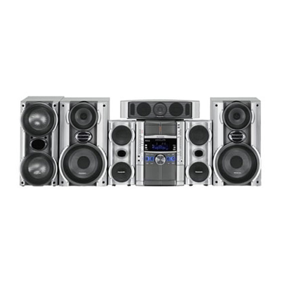
DVD Stereo System
SA-VK825DEE
Colour
(S)... Silver Type
Phone jack
Terminal
Mic jack
Sensitivity
Terminal
CASSETTE DECK SECTION
Type
Track system
Head Record/Playback
Erasure
Motor
Recording System
Erasing System
Tape Speed
Overall frequency response (+3, -6 dB) at DECK OUT
Normal
S/N Ratio
Wow and Flutter
Fast Forward and Rewind Time
DISC SECTION
Disc played [8 cm or 12 cm]
(1) DVD (DVD-Video, DVD-Audio, DivX
(2) DVD-RAM (DVD-VR, JPEG
(3) DVD-R (DVD-Video, DivX
(4) DVD-RW (DVD-Video, DVD-VR, DivX
+ R/RW (Video)
© 2005 Matsushita Electric Industrial Co. Ltd.. All
rights
reserved.
distribution is a violation of law.
ORDER NO. MD0507278C3
Stereo, 3.5 mm jack
0.7 mV, 600 Ω
Mono, 6.3 mm jack (2 system)
Auto-Reverse
4-Track, 2 Channel
Solid permalloy head
Double gap ferrite head
DC servo motor
AC Bias 100 kHz
AC Erase 100 kHz
35 Hz - 14 kHz
50 dB (A weighted)
0.18 % (WRMS)
Approx. 120 seconds with
C-60 cassette tape
* 6
,
*7
)
* 4 , * 7
* 5 , *7
* 6
*7
, MPEG4
,DivX
,
* 6
,
*7
)
* 6
,
*7
)
Unauthorized
copying
4.8 cm/s
)
and
Advertisement
Table of Contents

Related Manuals for Panasonic SA-VK825DEE


Summary of Contents for Panasonic SA-VK825DEE
- Page 1 ORDER NO. MD0507278C3 DVD Stereo System SA-VK825DEE Colour (S)... Silver Type Specifications AMPLIFIER SECTION Phone jack RMS Output Power: Dolby Digital Mode Terminal Stereo, 3.5 mm jack Main Mic jack 85 W per channel (4 Ω), 1 kHz, 10% THD 0.7 mV, 600 Ω...
- Page 2 Speakers: SB-VK82D (GC-S) Picture resolution: between 160 x 120 and 6144 x 4096 pixels (Sub sampling is 4:2:2 or 4:2:0) MPEG4 data recorded with Panasonic SD multi cameras or DVD video recorders. Conforming to SD VIDEO specifications (ASF standard)/ MPEG4 (Simple Profile) video system/G.726 audio system...
-
Page 3: Table Of Contents
SA-VK825DEE CONTENTS Page Page 1 Before Repair and Adjustment 15.6. Disassembly of Main P.C.B. 2 Protection Circuitry 15.7. Disassembly of Power Amp P.C.B. 3 Safety Precautions 15.8. Disassembly of Power P.C.B. 3.1. General Guidelines 15.9. Disassembly of Transformer P.C.B. 4 Prevention of Electro Static Discharge (ESD) to 15.10. -
Page 4: Before Repair And Adjustment
SA-VK825DEE 21.8. (J) CD Loading P.C.B. 25.1. Deck Mechanism (RAA3413-S) 22 Wiring Connection Diagram 25.2. DVD Loading Mechanism 23 Illustration of ICs, Transistors and Diodes 25.3. Cabinet 24 Terminal Function of IC 25.4. Electrical Parts List 24.1. IC2818 (C2CBJG000653) System Microprocessor 25.5. - Page 5 SA-VK825DEE Figure 1 3.1.2. Leakage Current Hot Check (See Figure 1) 1. Plug the AC cord directly into the AC outlet. Do not use an isolation transformer for this check. 2. Connect a 1.5kΩ, 10 watts resistor, in parallel with a 0.15µF capacitor, between each exposed metallic part on the set and a good earth ground such as a water pipe, as shown in Figure 1.
-
Page 6: Prevention Of Electro Static Discharge (Esd) To Electrostatically Sensitive (Es) Devices
SA-VK825DEE 4 Prevention of Electro Static Discharge (ESD) to Electrostatically Sensitive (ES) Devices Some semiconductor (solid state) devices can be damaged easily by electricity. Such components commonly are called Electrostatically Sensitive (ES) Devices. Examples of typical ES devices are integrated circuits and some field-effect transistors and semiconductor “chip”... -
Page 7: Precaution Of Laser Diode
SA-VK825DEE 6 Precaution of Laser Diode Caution : This product utilizes a laser diode with the unit turned "ON", invisible laser radiation is emitted from the pick up lens. Wavelength : 785 nm(CD)/662 nm(DVD) Maximum output radiation power from pick up : 100 µW/VDE Laser radiation from pick up unit is safety level, but be sure the followings: 1. -
Page 8: Cautions To Be Taken When Handling Optical Pickup
SA-VK825DEE 7 Cautions to be taken when handling Optical Pickup The laser diode used inside optical pickup could be destroyed due to static electricity as a potential difference is caused by electrostatic load discharged from clothes or human body. Handling the parts carefully to avoid electrostatic destruction during repair. -
Page 9: Accessories
SA-VK825DEE 8 Accessories Remote control AC cord FM antenna AM antenna Video cable Microphone... -
Page 10: Operation Procedures
SA-VK825DEE 9 Operation Procedures... - Page 11 SA-VK825DEE...
-
Page 12: Disc Information
SA-VK825DEE 10 Disc information... - Page 13 SA-VK825DEE...
-
Page 14: About Highmat
SA-VK825DEE 11 About HighMAT 11.1. What’s HighMAT? Consumers worldwide are using PCs to create their own collections of music, photos and even video by burning them onto CDs. But how these collections can be experienced across different devices can be confusing to navigate, time consuming to access for a DVD player, and be incomplete in terms of music information available to the customer. -
Page 15: Benefits Of Highmat
SA-VK825DEE A Solution Created: HighMAT delivers a better digital media access experience by creating a standard approach for PCs to structure digital media on various physical formats and for playback devices to read the data. 11.3. Benefits of HighMAT? Conventional... - Page 16 SA-VK825DEE...
- Page 17 SA-VK825DEE HighMAT is now available for CD Burning and in Leading DVD PlayersHighMAT is a new technology that is now available in leading software and consumer electronic devices to dramatically improve the digital media experience when you create homemade CDsHighMAT delivers a simple, standardized way for PC software and consumer electronics devices to talk to each other and work better together.
-
Page 18: Optical Pickup Self-Diagnosis And Replacement Procedure
SA-VK825DEE 12 Optical Pickup Self-Diagnosis and Replacement Procedure 12.1. Optical Pickup Breakdown diagnosis This unit is equipped with the optical pickup self-diagnosis function and the tilt adjustment check function. Follow the procedure described below during repair in order to perform self-diagnosis and tilt adjustment effectively. Especially when “NO DISC” is displayed, be sure to apply the self-diagnosis function before replacing with an optical pickup. -
Page 19: Self-Diagnosis Function
SA-VK825DEE 13 Self-Diagnosis Function This unit is equipped with the self-diagnosis function, which displays an error when it occurs, for use during servicing. 13.1. Entering into Self-Diagnostic Mode 13.2. Automatic Displayed Error Codes 13.2.1. Automatic Display Function For a power unit error, the code is automatically displayed. -
Page 20: Service Mode Table
SA-VK825DEE If several errors are detected, press the button to display each. 13.3.2. Re-Display · Press the power button to turn off the power, and then turn on the power. · The details of self diagnosis are stored in the unit memory. - Page 21 SA-VK825DEE Item Operational Condition Details Display TO Exit Mode and Key Function Jitter display While player Jitter display xxx/yyy zz (display1/display2) Press the STOP stopped and no disc is Measures displays jitter. button inserted, press and hold Measurement repeated every : Jitter display mode player.
- Page 22 SA-VK825DEE Item Operational Condition Details Display TO Exit Mode and Key Function Measurement of CD While player Measurement of CD laser current /xxx yyyy Automatically exits laser current electricity stopped and no disc is electricity (display1/display2) the mode after five...
-
Page 23: Cr16 Mechanism Ageing Mode
SA-VK825DEE Item Operational Condition Details Display TO Exit Mode and Key Function Spindle use time While player Spindle motor usage time T2_00000 Automatically exits stopped and no disc is the mode after five inserted, press and hold The four-digit number is shown by seconds. -
Page 24: Things To Do After Repair
SA-VK825DEE 13.9. Things to Do After Repair Follow the procedure described below after repair. 1. While the power is on, press the button to close the tray. 2. Press the power button to turn off the power. 3. Unplug the power cable. -
Page 25: Using Recovery Disc
SA-VK825DEE Version upgrade process: Renewal of firmware for improvement of operational range and performance 14.4. Using Recovery Disc 14.4.1. Recovery Process 1. Insert the recovery disc (RFKZD03R005) to the player to replay. 2. The recovery process automatically starts, and a message of completion prompts on the screen. -
Page 26: Disassembly And Assembly Of Main Component
SA-VK825DEE 15 Disassembly and Assembly of Main Component “ATTENTION SERVICER” Some chassis components may have sharp edges. Be careful when disassembling and servicing. 1. This section describes procedures for checking the operation of the major printed circuit boards and replacing the main components. -
Page 27: Disassembly Flow Chart
SA-VK825DEE 15.2. Disassembly flow chart The following chart is the procedure for disassembling the casing and inside parts for internal inspection when carrying out the servicing. To assemble the unit, reverse the steps shown in the chart as below. -
Page 28: Disassembly Of Top Cabinet
SA-VK825DEE 15.3. Disassembly of Top Cabinet Step 1 Remove 3 screws at each side and 5 screws at rear panel. Step 2 Lift up both sides of the top cabinet, push the top cabinet towards the rear to remove the top cabinet. -
Page 29: Disassembly Of Main P.c.b
SA-VK825DEE Step 3 Release the claws on both ends, and remove the DVD changer unit. Step 5 Remove 2 screws. Step 6 Remove the DVD chassis. Step 7 Lay the unit. · For disassembly of DVD mechanism unit, please refer to Section 15.16 of this manual. -
Page 30: Disassembly Of Power Amp P.c.b
SA-VK825DEE Step 2 Lift up Main P.C.B. by disconnecting connectors CN2801 & CN2802 as arrow shown above. 15.7. Disassembly of Power Amp P.C.B. · Follow the (Step 1) - (Step 2) of Item 15.3 - Disassembly of Top Cabinet · Follow the (Step 1) of Item 15.4 - Disassembly of Rear Panel ·... -
Page 31: Disassembly Of Power P.c.b
SA-VK825DEE · Replacement of the Power Amp IC Power Amp P.C.B. Repeat Step 1 - Step 3 of Section 15.7 - Disassembly of 15.8. Disassembly of Power P.C.B. · Follow the (Step 1) - (Step 2) of Item 15.3 - Disassembly of Top Cabinet ·... -
Page 32: Disassembly Of Transformer P.c.b
SA-VK825DEE 15.9. Disassembly of Transformer P.C.B. · Follow the (Step 1) - (Step 2) of Item 15.3 - Disassembly of Top Cabinet · Follow the (Step 1) of Item 15.4 - Disassembly of Rear Panel · Follow the (Step 1) - (Step 4) of Item 15.5 - Disassembly of DVD Changer Unit ·... - Page 33 SA-VK825DEE Step 4 Remove the front panel unit. Note: Ensure 2 claws on bottom chassis is properly and fully catched to the front panel holes.
-
Page 34: Disassembly For Mic P.c.b. & Panel P.c.b
SA-VK825DEE 15.11. Disassembly for Mic P.C.B. & Panel P.C.B. · Follow the (Step 1) - (Step 2) of Item 15.3 - Disassembly of Top Cabinet · Follow the (Step 1) - (Step 4) of Item 15.5 - Disassembly of DVD Changer Unit ·... -
Page 35: Disassembly Of Deck Mechanism Unit
SA-VK825DEE 15.12. Disassembly of Deck Mechanism Unit · Follow the (Step 1) - (Step 2) of Item 15.3 - Disassembly of Top Cabinet · Follow the (Step 1) - (Step 4) of Item 15.5 - Disassembly of DVD Changer Unit ·... -
Page 36: Replacement For Traverse Deck
SA-VK825DEE 15.14. Replacement for Traverse Deck · Follow the (Step 1) - (Step 2) of Item 15.3 - Disassembly of Top Cabinet · Follow the (Step 1) - (Step 7) of Item 15.5 - Disassembly of DVD Changer Unit Step 1 Move ribs at both sides to the arrow direction (The vertical rack (R) slides and the groove opens). -
Page 37: Replacement For Optical Pickup Unit (Dvd Mechanism)
SA-VK825DEE 15.15. Replacement for Optical Pickup Unit (DVD mechanism) · Follow the (Step 1) - (Step 2) of Item 15.3 - Disassembly of Top Cabinet · Follow the (Step 1) - (Step 7) of Item 15.5 - Disassembly of DVD Changer Unit ·... - Page 38 SA-VK825DEE Step 10 Remove the catch of the drive rack, and take out the drive rack. Step 11 Place the convex part of an optical pickup to the concave part of a traverse base, then take out the optical pickup.
-
Page 39: Procedure For Removing Cd Loading Mechanism
SA-VK825DEE 15.16. Procedure for removing CD loading mechanism 1. Turn off by pressing power SW in the body. 2. Unplug AC power cord after the indication of [GOOD-BYE], then disassemble the body. 3. Disassemble the body, and take out CD loading mechanism. - Page 40 SA-VK825DEE...
- Page 41 SA-VK825DEE 15.17.3. Replacement for the traverse deck · Follow the (Step 1) - (Step 10) of item 15.17.2.
- Page 42 SA-VK825DEE 15.17.4. Disassembly for CD loading unit · Follow the (Step 1) - (Step 10) of item 15.17.2. · Follow the (Step 1) - (Step 4) of item 15.17.3.
- Page 43 SA-VK825DEE...
- Page 44 SA-VK825DEE...
-
Page 45: Cr16 Mechanism Assembly Procedure
SA-VK825DEE 15.18. CR16 mechanism assembly procedure The following specified greases and/or oil must be applied when some specific parts are changed. 1. Floil grease (VFK1298) : The floil grease must be applied to tray, tray (L) and tray (R). 2. Hanarl oil (VFK1700) : The hanarl oil must be applied to... - Page 46 SA-VK825DEE...
- Page 47 SA-VK825DEE...
- Page 48 SA-VK825DEE...
- Page 49 SA-VK825DEE...
- Page 50 SA-VK825DEE...
- Page 51 SA-VK825DEE...
- Page 52 SA-VK825DEE...
- Page 53 SA-VK825DEE...
- Page 54 SA-VK825DEE...
- Page 55 SA-VK825DEE...
- Page 56 SA-VK825DEE...
-
Page 57: Disassembly For Traverse Unit
SA-VK825DEE 15.19. Disassembly for Traverse Unit · Follow the (Step 1) - (Step 10) of item 15.17.2 · Follow the (Step 1) - (Step 4) of item 15.17.3... -
Page 58: Replacement For Cassette Lid
SA-VK825DEE 15.20. Replacement for cassette lid · Follow the (Step 1) - (Step 2) of Item 15.3 - Disassembly of Top Cabinet Step 1 Lift up the lever upward, open the cassette deck. (For DECK1 and DECK2) Step 2 Push up the cassette lid (L/R) in the direction of arrow. -
Page 59: Rectification For Tape Jam Problem
SA-VK825DEE 15.21. Rectification for tape jam problem · Follow the (Step 1) - (Step 2) of Item 15.3 - Disassembly of Top Cabinet Step 1 If a cassette tape cannot be removed from the deck (the tape is caught by the capstan or pinch roller during playback or recording), rotate the flywheel F in the direction of the arrow to remove it. -
Page 60: Checking For Major P.c.bs
SA-VK825DEE 16 Checking for major P.C.Bs Note: Checking of all major P.C.Bs (Main P.C.B., Panel P.C.B., Transformer P.C.B., Deck P.C.B., Deck Mechanism P.C.B., Mic P.C.B., Power P.C.B. and Power Amp P.C.B.) can be carried out using below procedures. For the disassembling procedures, refer to Section 15. -
Page 61: Checking Of Transformer P.c.b
SA-VK825DEE 16.2. Checking of Transformer P.C.B. 1. Remove Top Cabinet. 2. Disassemble DVD Changer Unit. 3. Connect FFC cables (CN2810 & CN2813) from Main P.C.B. -
Page 62: Checking Of Panel, Deck & Deck Mechanism P.c.b
SA-VK825DEE 16.3. Checking of Panel, Deck & Deck Mechanism P.C.B. 1. Remove Top Cabinet. 2. Disassemble DVD Changer Unit. 3. Disassemble Front Panel Unit. 4. Remove volume knob and Mic Jack Holder. 5. Disassemble Panel P.C.B. 6. Disassemble Deck Mechanism Unit. -
Page 63: Checking Of Power P.c.b
SA-VK825DEE 16.4. Checking of Power P.C.B. 1. Remove Top Cabinet and Rear Panel. 2. Disassemble DVD Changer Unit. 3. Remove 4 screws at Transformer P.C.B.. 4. Remove 2 screws at heat sink and 1 screw at Power P.C.B. 5. Flip the Power P.C.B. -
Page 64: Measurements And Adjustments
SA-VK825DEE 17 Measurements and Adjustments 17.1. Cassette Deck Section 17.1.2. Tape Speed Adjustment (Deck 1/2) · Measurement Condition 1. Set the tape edit button to “NORMAL” position. − − − − Reverse-mode selector switch: 2. Insert the test tape (QZZCWAT) to DECK 2 and playback (FWD side) the middle portion of it. -
Page 65: Tuner Section
SA-VK825DEE 17.1.4. Bias Frequency Adjustment (Deck 1/2) 1. Set the unit to “AUX” position. 2. Insert the Normal blank tape (QZZCRA) into DECK 2 and set the unit to “REC” mode (l use “REC/STOP” key). 3. Adjust L1002 so that the output frequency is within the standard value. -
Page 66: Alignment Points
SA-VK825DEE 17.3. Alignment Points 17.3.1. Cassette Deck Section 17.3.2. Adjustment Point... -
Page 67: Block Diagram
SA-VK825DEE 18 Block Diagram OPTICAL PICKUP LD(DVD) SPINDLE MOTOR UNIT LD(CD) Q8552 Q8562 SWITCH SWITCH BIAS IC8251 C0GBG0000048 OPIN+ MOTOR DRIVE LDIN BIAS2 TRIN Q8551 Q8561 SWITCH SWITCH QR8571 SUPPLY CONTROL SWITCH 130 131 129 132 127 113 114 133 134 135 118 136 117 137 116 138 115 DV3.2 LSI... - Page 68 SA-VK825DEE IC8601 C0EBA0000029 VOLTAGE DETECTOR IC8051 IC8651 C3ABPG000145 XRESET RFKWMH90E160 64 SDRAM IC 16M FLASH ROM IC 2,4,5,7,8,10,11, 22-26, 9, 16, 1~8, 29-36, 13,42,44,45,47, 29-35 17, 48 18-25 38-45 IC8606 48,50,51,53 C0EBE0000455 RESET IC 198~203, 206~213, 41, 54, 18, 42, 43,...
- Page 69 SA-VK825DEE 27(26) 22(21) 20(19) Q8335 Q8321 QR8111 IC8111 C0CBCBD00018 SWITCH SWITCH SWITCH POWER SUPPLY Q8331 Q8341 Q8325 IC8421 SWITCH SWITCH SWITCH C0FBBK000050 AUDIO DAC 11~13 IC8695 IC8691 C0JBAA000346 C0JBAA000346 AND GATE AND GATE LOGIC IC LOGIC IC QR8420 MUTING SWITCH 170~172 DV3.2 LSI...
- Page 70 SA-VK825DEE AM ANT FM ANT Z2620 CF2601 CF2602 Q1 (RF AMP) Q2601 MIXER IF AMP D2602 L2602 L2601 BUFFER (FM) DECODER RM AMP BUFFER PHASE PILOT CANCEL STEREO LEVEL S-CURVE SWITCH AM/FM COMP BUFFER TUNING DRIVE PILOT IC2601 X2602 LA1833NMNTLM...
- Page 71 SA-VK825DEE FL6800 FROM POWER FL DISPLAY TRANSFORMER 6~40 41~49 16~23, 1~2, 25~51 58~64 IC6803 C0HBB0000039 FL DRIVER RM11 RM21 UP/DOWN MOTOR LOADING MOTOR PLLDA IC11 IC21 ST/DO C0GAG0000007 C0GAG0000007 UP/DOWN LOADING MOTOR DRIVER MOTOR DRIVER PLLCLK PLL_CE C2CBJG000653 IC2818 MICROPROCESSOR...
- Page 72 SA-VK825DEE IC1001 AN7348S-E1 P.B EQ/REC AMP/ ALC/TPS AMP 24(23) (DECK 1) P.B. HEAD 1(2) 20(5) 22(3) 21(4) 17(8) (DECK 2) R/P HEAD 18(7) LOGIC L/H NOR/CrO & HI/LO LOGIC RIPPLE LOGIC REJECTION REC/PB Q2704 SWITCH (DECK 2) ERASE HEAD L1002...
- Page 73 SA-VK825DEE JK2802 COMPONENT VIDEO BLUE CbOUT GREEN CyOUT VIDEO YELLOW VOUT CyIN IC2006 C9ZB00000466 CrOUT VIDEO IC CB_B CbIN JK2801 S.VIDEO OUT YOUT CR_R COUT CrIN DVD_CLK DVD_STAT Q2838 SWITCH IC2803 DVD_CMD C0DBEZG00021 Q2920 REGULATOR MIX_MUTE MUTING SWITCH Q2806 Q9504...
- Page 74 SA-VK825DEE IC2814 Q6817 Q6806, Q6807 KIA4558FEL IC2813 76(75) DUAL OP-AMP IC2800 C1BB00001012 LIMITTER LOUT(R) 15(14) KARAOKE IC C1BB00000979 64(63) JK6802 5(3) ANALOG SURROUND IC 7(1) 6(7) LCIN(R) MIC2 COUT 6(2) SOUT Q2813 JK6800 JK2803 MUTING MIC1 SWITCH LINE OUT Q2814...
- Page 75 SA-VK825DEE 65(66) INC1(2) 25(23) OUTLS(R) 63(64) JK2803 INB1(2) 61(62) INFLA(B) DVDFL(R) 75(76) INCA IC2815 DVDCNT INLSA(R) KIA4558FEL DUAL OP-AMP DVDSL(R) 78(79) IND1(2) OUTC SUBW INSUBA IC2812 DVD_MIXL(R) C1BB00000845 67(68) IND1(2) ASP IC OUTSUB Q2919 MIX_MUTE MUTING SWITCH 59(60) LOUT1(2) IC2819...
- Page 76 SA-VK825DEE FILTER 16(15) -IN21(22) 3(6) OUT21(22) IC5801 -IN11 SUR_L(R) RSN315H42C-P OUT11 POWER AMP -IN12 ACDET OUT12 JK9502 FILTER CENTER SUBWOOFER JK9503 FILTER FRONT L(R) IC5001 FILTER 10(14) LATCH -IN_L(R) RSN35H2B-P POWER AMP ACDET 4(1) OUTL(R) Q5811 Q5801, Q5810 SWITCH SWITCH...
- Page 77 SA-VK825DEE JK6801 HEADPHONE HP _SW HP _OUT Q2710 SYNC SYNCHRONISING SWITCH Q2702 RESET SWITCH Q9501 D9512,D9517 SYSTEM 6V VOLTAGE REGULATOR Q9502 SYSTEM 6V VOLTAGE REGULATOR Q5802, Q5805 SWITCH Q5809 9V VOLTAGE REGULATOR T9501 FP5833 FP9502 T9500 Q5803 D9518-D9521 15V VOLTAGE...
-
Page 78: Voltage Measurement
SA-VK825DEE 19 Voltage Measurement This section is not available at time of issue. -
Page 79: Schematic Diagram
SA-VK825DEE 20 Schematic Diagram (All schematic diagrams may be modified at any time with the Secondary trouble can be prevented by taking care during development of the new technology) repair. · Cover the parts boxes made of plastics with aluminium foil. -
Page 80: Optical Pickup Unit Circuit
SA-VK825DEE 20.1. Optical Pickup Unit Circuit SCHEMATIC DIAGRAM - 1 OPTICAL PICKUP UNIT CIRCUIT : +B SIGNAL LINE : CD-DA SIGNAL LINE J0JBC0000105 TO ACT J0JBC0000105 GND (IM) DVD MODULE CIRCUIT VREF2(RF-) (FP8501) ON PIN (DVD) SCHEMATIC LD (CD) DIAGRAM - 2... -
Page 81: A) Dvd Module Circuit
SA-VK825DEE 20.2. (A) DVD Module Circuit SCHEMATIC DIAGRAM - 2 : +B SIGNAL LINE : CD-DA SIGNAL LINE DVD MODULE CIRCUIT TRV-I-SW D+5V FODRV TRDRV C8251 6.3V220 TL8201 VHALF C8262 C8261 R8230 BIAS1 LDCNT 2.2K CL8262 SPMUTE VIN1 MUTE3 R8231... - Page 82 SA-VK825DEE SCHEMATIC DIAGRAM - 3 : +B SIGNAL LINE DVD MODULE CIRCUIT D+3.3V IC8111 C0CBCBD00018 3.3 REGULATOR IC TL8111 D+5V C8111 C8112 IC8111 RX8111 (22K x 2) C8113 470P Cont QR8111 XP0621400L SWITCH QR8571 D+1.2V UNR511V00L CL8571 SUPPLY CONTROL SWITCH...
- Page 83 SA-VK825DEE SCHEMATIC DIAGRAM - 4 : MAIN SIGNAL LINE : +B SIGNAL LINE : DVD VIDEO SIGNAL LINE DVD MODULE CIRCUIT FP8101 VGND Y/PY/G Y/PY/G LB8303 J0JBC0000042 VGND CB/PB/B CB/PB/B LB8304 J0JBC0000042 VGND CR/PR/R CR/PR/R LB8305 J0JBC0000042 VGND LB8301 J0JBC0000042...
- Page 84 SA-VK825DEE SCHEMATIC DIAGRAM - 5 : +B SIGNAL LINE : DVD VIDEO SIGNAL LINE DVD MODULE CIRCUIT EXADR15 EXADR16 EXADR14 XBYTE EXADR13 EXADR12 EXDT15 DQ15/A-1 EXADR11 EXDT7 EXADR10 EXDT14 DQ14 EXADR9 EXDT6 EXADR8 EXDT13 DQ13 EXADR19 EXDT5 EXADR20 EXDT12 DQ12...
- Page 85 SA-VK825DEE SCHEMATIC DIAGRAM - 6 : +B SIGNAL LINE DVD MODULE CIRCUIT C8051 MDQ0 MDQ15 DQ15 C8052 VDDQ VSSQ MDQ1 MDQ14 DQ14 MDQ2 DQ13 C8057 RX8012 (82 x 4) VSSQ VDDQ MDQ3A MDQ3 CL8053 MDQ12 MDQ3 DQ12 MDQ2A C8018 MDQ2...
- Page 86 SA-VK825DEE SCHEMATIC DIAGRAM - 7 : +B SIGNAL LINE DVD MODULE CIRCUIT RX8018 (22 x 2) RX8017 (82 x 4) MDQ18 TRCDATA1 TRCDATA0 VDD33 TRCCLK MDQ28 EXTRGO MDQ19 SDATA MDQ27 SCLOCK MDQ20 EXTRG1 VDD33 VDD33 MDQ26 VDIO0 MDQ21 VDIO1 MDQ25...
- Page 87 SA-VK825DEE SCHEMATIC DIAGRAM - 8 : CD-DA SIGNAL LINE : DVD VIDEO SIGNAL LINE : +B SIGNAL LINE : DVD AUDIO SIGNAL LINE DVD MODULE CIRCUIT R8041 LB8011 J0JHC0000045 D+3.3V D+1.2V C8001 C8011 LB8001 4V330 6.3V100 J0JHC0000045 RX8031 (4.7K x 2)
-
Page 88: B) Main (Tuner) Circuit
SA-VK825DEE 20.3. (B) Main (Tuner) Circuit SCHEMATIC DIAGRAM - 9 : +B SIGNAL LINE : FM SIGNAL LINE : AM SIGNAL LINE MAIN (TUNER) CIRCUIT : FM/AM SIGNAL LINE : FM OSC SIGNAL LINE : AM OSC SIGNAL LINE R3604... -
Page 89: B) Main Circuit
SA-VK825DEE 20.4. (B) Main Circuit SCHEMATIC DIAGRAM - 10 : AUX SIGNAL LINE : DVD VIDEO SIGNAL LINE MAIN CIRCUIT : +B SIGNAL LINE : MAIN SIGNAL LINE : VIDEO SIGNAL LINE Q2814 C2855 R2846 B1GDCFGA0018 50V4.7 R2849 MUTING SWITCH... - Page 90 SA-VK825DEE SCHEMATIC DIAGRAM - 11 CD LOADING CIRCUIT (CN1) ON : +B SIGNAL LINE : DVD VIDEO SIGNAL LINE SCHEMATIC DIAGRAM - 26 MAIN CIRCUIT : -B SIGNAL LINE : MAIN SIGNAL LINE CN2810 14 13 12 11 10 D2911...
- Page 91 SA-VK825DEE SCHEMATIC DIAGRAM - 12 TRANSFORMER CIRCUIT (H9502/W9502) : +B SIGNAL LINE : MIC SIGNAL LINE ON SCHEMATIC DIAGRAM - 25 MAIN CIRCUIT : -B SIGNAL LINE : MAIN SIGNAL LINE CN2814 C2108 R2109 R2108 50V47 3.3K C2106 R2106 C2104...
- Page 92 SA-VK825DEE SCHEMATIC DIAGRAM - 13 : +B SIGNAL LINE MAIN CIRCUIT : -B SIGNAL LINE : MAIN SIGNAL LINE C2602 C2219 C2306 C2406 C2119 50V4.7 50V2.2 50V2.2 50V4.7 Q2815 Q2816 R2615 R2218 R2306 R2406 R2118 6.8K 1.8K 1.8K R2852 R2620...
- Page 93 SA-VK825DEE SCHEMATIC DIAGRAM - 14 BOTTOM : +B SIGNAL LINE : AUX SIGNAL LINE : FM/AM SIGNAL LINE MAIN CIRCUIT : -B SIGNAL LINE : MAIN SIGNAL LINE : TAPE PLAYBACK SIGNAL LINE CN2816 Q2916 Q2915 2SB0709AHL 2SB0709AHL D2917, D2919...
- Page 94 SA-VK825DEE SCHEMATIC DIAGRAM - 15 : +B SIGNAL LINE : FM/AM SIGNAL LINE MAIN CIRCUIT : -B SIGNAL LINE : MAIN SIGNAL LINE : TAPE PLAYBACK SIGNAL LINE CN2815 Q2911 Q2912 D2914, D2916 2SB0709AHL 2SB0709AHL B0ACCK000005 FAN MOTOR DRIVE FAN MOTOR DRIVE...
- Page 95 SA-VK825DEE SCHEMATIC DIAGRAM - 16 MAIN CIRCUIT : +B SIGNAL LINE R2687 R2748 VREF+ BASS LEDCONT R2683 100K R2684 100K PHOTO_1 R2791 PHOTO_2 R2792 DECK2 R2797 KEY1 R2672 R2798 KEY2 KEY3 R2708 C2718 470P R2723 R2086 R2658 C2721 C2719 0.01 0.01...
- Page 96 SA-VK825DEE SCHEMATIC DIAGRAM - 17 MAIN CIRCUIT : +B SIGNAL LINE C2708 R2788 100P 100K C2709 C2742 100P 0.01 C2710 100P R2075 R2074 DVD_MUTE R2790 MODEL_ DVD_MUTE R2776 ASP_CK BASS ASP_CK R2775 ASP_DA MIC_1L ASP_DA R2774 WIDE_1 MIC_2L WIDE_1 EFP_CE...
- Page 97 SA-VK825DEE SCHEMATIC DIAGRAM - 18 : +B SIGNAL LINE : MIC SIGNAL LINE MAIN CIRCUIT : -B SIGNAL LINE : MAIN SIGNAL LINE HPOUT_FL HPOUT_FL HPGND HPOUT_FR HPOUT_FR MICGND HP_MUTE HP_MUTE KEY1 KEY1 KEY2 KEY2 KEY3 KEY3 GND2 JOG_A JOG_A...
-
Page 98: C) Panel Circuit & (D) Mic Circuit
SA-VK825DEE 20.5. (C) Panel Circuit & (D) Mic Circuit SCHEMATIC DIAGRAM - 19 : +B SIGNAL LINE : MIC SIGNAL LINE PANEL CIRCUIT : -B SIGNAL LINE : MAIN SIGNAL LINE L6802, L6803 L6804, L6808 G0C101JA0052 G0C100JA0052 L6808 HP_SW L6802... - Page 99 SA-VK825DEE SCHEMATIC DIAGRAM - 20 : +B SIGNAL LINE : MIC SIGNAL LINE PANEL CIRCUIT : -B SIGNAL LINE : MAIN SIGNAL LINE FL6800 A2BD00000125 FL DISPLAY 54 53 52 51 50 49 48 47 46 45 44 43 42 41 40 39 38 37 36 35 34 33 32 31 30 29 28 27 26 25 24 23 22 21 20 19 18 17 16 15 14 13 12 11 10 9 8 7 6 5 4 3...
-
Page 100: E) Deck Circuit & (F) Deck Mechanism Circuit
SA-VK825DEE 20.6. (E) Deck Circuit & (F) Deck Mechanism Circuit SCHEMATIC DIAGRAM - 21 : +B SIGNAL LINE : PLAYBACK SIGNAL LINE DECK CIRCUIT : RECORD SIGNAL LINE C1038 R1055 C1057 220P C1034 2.2K 1000P 50V3.3 C1044 10V33 R1101 R1100... - Page 101 SA-VK825DEE SCHEMATIC DIAGRAM - 22 MAIN CIRCUIT (CP6803) ON SCHEMATIC : +B SIGNAL LINE : PLAYBACK SIGNAL LINE DIAGRAM - 15 DECK CIRCUIT : RECORD SIGNAL LINE CN1001 R1098 R1060 R1057 R1091 2.2K R1092 R1049 R1084 W1002 2.2K Q1017 B1AARC000003...
-
Page 102: G) Power Circuit
SA-VK825DEE 20.7. (G) Power Circuit SCHEMATIC DIAGRAM - 23 : +B SIGNAL LINE POWER CIRCUIT : -B SIGNAL LINE : MAIN SIGNAL LINE C9520 0.047 IC5001 R5205 C5203 C5202 IC5001 RSN35H2B-P R9523 POWER HIC L9502 R9528 FR_GND C5102 C9527 RIGHT L9507 0.047... -
Page 103: H) Power Amp Circuit
SA-VK825DEE 20.8. (H) Power Amp Circuit SCHEMATIC DIAGRAM - 24 : +B SIGNAL LINE POWER AMP CIRCUIT : -B SIGNAL LINE : MAIN SIGNAL LINE SUB_IN SUR_R_IN CENT_IN SUR_L_IN POWER R5819 CIRCUIT SUR_L_OUT 330K (H5900) ON SUR_R_OUT SCHEMATIC C5836 DIAGRAM - 23... -
Page 104: I) Transformer Circuit
SA-VK825DEE 20.9. (I) Transformer Circuit SCHEMATIC DIAGRAM - 25 : +B SIGNAL LINE TRANSFORMER CIRCUIT : -B SIGNAL LINE R9517 T9500 G4C8AGK00003 AC_IN +VccH D9504 +VccH B0FBAM000009 +VccL C9501 AC_GND AC_GND R9836 -VccL POWER -VccH D9518 - D9521 CIRCUIT B0EAKM000038... -
Page 105: J) Cd Loading Circuit
SA-VK825DEE 20.10. (J) CD Loading Circuit SCHEMATIC DIAGRAM - 26 CD LOADING CIRCUIT : +B SIGNAL LINE IC11 C0GAG0000007 UP/DOWN MOTOR DRIVE 0.01 16V100P RM11 UP/DOWN MOTOR CHANGE BOTTOM OPEN B3NAA0000068 +7.5V SENSOR STOCK PGND CR16 SWITCH DGND UP/DOWN F... -
Page 106: Printed Circuit Board
SA-VK825DEE 21 Printed Circuit Board 21.1. (A) DVD Module P.C.B. (Side: A & B ) DVD MODULE P.C.B (REP3908B) C8530 LB8530 IC8251 C8572 RX8532 C8531 LB8257 IC8601 RX8531 C8261 R8262 R8264 Q8551 IC8606 R8562 QR8571 R8552 Q8561 CL8034 R8003 C8521... - Page 107 SA-VK825DEE DVD MODULE P.C.B (REP3908B) FP8531 TO OPTICAL PICKUP UNIT R8263 C8262 R8261 C8258 C8253 C8257 Q8552 C8251 Q8562 R8554 C8554 R8558 R8553 R8563 R8564 R8565 R8559 C8561 C8551 C8564 C8550 CL8006 L8550 IC8611 L8330 C8501 C8201 C8516 C8515 C8113...
-
Page 108: B) Main P.c.b
SA-VK825DEE 21.2. (B) Main P.C.B. MAIN P.C.B (REPX0486D) LINE OUT FM ANT AM ANT JK2803 JK2601 IC2815 W2881 R2848 Q2818 1 2 3 W2417 W2626 R2307 R2236 R2235 W2412 C2605 R2623 R2508 W2127 C2604 W2128 TUNER PACK R2622 R2135 Q2820... - Page 109 SA-VK825DEE S. VIDEO COMPONENT AM ANT VIDEO OUT JK2802 JK2801 C2842 C3623 L2816 C2849 C2848 C2847 2-PR C2846 5-PB R2834 L2811 W3011 L2815 R2816 R2825 C2850 C2851 L2814 R2828 R2831 R2807 R2832 R2824 R2823 C2039 K2902 C2991 Q2915 Q2913 C2434...
-
Page 110: C) Panel P.c.b
SA-VK825DEE 21.3. (C) Panel P.C.B. PANEL P.C.B (REPX0487A) S6819 OPEN/CLOSE R6963 S6820 DISC CHANGE R6964 S6821 DISC 5 R6965 FL6800 H6800 S6822 DISC 4 R6966 S6823 W6854 DISC 3 W6855 S6824 DISC 2 W6857 W6853 C6894 Z6800 W6856 W6866 W6878... - Page 111 SA-VK825DEE S6810 AC IN R6937 R6829 S6811 DISC CHECK R6938 S6812 MULTI REMASTER CN6811 R6939 R6997 W6880 S6813 W6867 SUPER SURROUND C6855 W6865 W6863 D6802 Q6803 W6858 R6940 W6861 W6866 W6878 W6913 W6860 S6818 W6864 SOUND EQ W6862 Q6805 W6870...
-
Page 112: D) Mic P.c.b. & (K) Tuner Pack P.c.b
SA-VK825DEE 21.4. (D) Mic P.C.B. & (K) Tuner Pack P.C.B. MIC P.C.B (REPX0487A) MIC1 MIC2 JK6802 JK6800 R6891 Q6817 K6806 C6872 R6890 Q6807 C6875 C6871 R6886 W6890 R6982 C6866 C6811 R6981 R6991 W6891 Q6806 H6805 R6992 R6995 TUNER PACK P.C.B (REP1999B) -
Page 113: E) Deck P.c.b. & (F) Deck Mechanism P.c.b
SA-VK825DEE 21.5. (E) Deck P.C.B. & (F) Deck Mechanism P.C.B. DECK P.C.B DECK MECHANISM P.C.B. (REPX0331E) (REPX0321B) R1024 IC1004 C1006 C1009 R1027 CS1002 TO R/P HEAD TP10 Q1003 TP4 x J1002 L1002 TP3 x TP11 R1004 J1003 C1002 C1026 C1011... -
Page 114: G) Power P.c.b. & (H) Power Amp P.c.b
SA-VK825DEE 21.6. (G) Power P.C.B. & (H) Power Amp P.C.B. POWER P.C.B (REPX0488C) Q5802 Q5809 Q5803 Q5804 C5804 R5814 W5879 C5811 C5809 C5806 R5828 FP5833 R5102 R5823 D5801 Q5807 0.4A R5813 W5857 H9500 W5878 R5200 R5892 Q5806 W5887 R5830 C5808... - Page 115 SA-VK825DEE IC5001 L9502 R5102 W5847 C5202 D5820 R9523 JK9503 L9507 W5857 W5849 C5102 5-FR R5205 R5200 RIGHT SPEAKER R9528 R5105 6-GND C5834 R5206 R5100 3-LOW_R W5860 SUBWOOFER W5833 4-GND 5817 W5834 W5861 Q5801 1-SUB_W_R LEFT SPEAKER W5859 W5835 C5605 Q5810...
-
Page 116: I) Transformer P.c.b
SA-VK825DEE 21.7. (I) Transformer P.C.B. TRANSFORMER P.C.B (REPX0489E) CAUTION RISK OF ELECTRIC SHOCK AC VOLTAGE LINE. PLEASE DO NOT TOUCH THIS P.C.B H9502/W9502 W9500 R9507 C9514 IC9500 Q9504 R9522 VK82D K5802 R9516 D9503 K5807 VK825D/EE R9510 C9515 W9600 R9517 R9509... - Page 117 SA-VK825DEE 21.8. (J) CD Loading P.C.B. CD LOADING P.C.B (REP3569A) CHANGESW RM21 LOADING_MOTOR STOCKSW PLAYSW RM11 UP/DOWN_ MOTOR IC21 IC11 OPENSW BOTTOMSW...
- Page 118 SA-VK825DEE 22 Wiring Connection Diagram CN6811 1 ..29 2 ..30 1..7 H6800 Z6800 H6810 PANEL P.C.B.
- Page 119 SA-VK825DEE DECK P.C.B. SOLDER SIDE CN2801 CN2802 1... . 12 1... . 12 CS1002 CP6803 (DECK 2) R/P HEAD, MOTOR...
- Page 120 SA-VK825DEE 23 Illustration of ICs, Transistors and Diodes RSN315H42C-P AN7348S-E1 (24P) C1AA00000612 C0FBBK000050 (28P) C0HBB0000039 (64P) C1BB00000086 (18P) MN2DS0009AP (256P) C3ABPG000145 (54P) C2CBJG000653 (100P) KIA4558FEL(8P) C1BB00000845 (56P) LA1833NMNTLM (24P) C1BB00000801 (80P) LC72131MDTRM (20P) CNB13030R2AU C0GBG0000048 C0EBA0000029 C0CBCBD00018 (8P) RSN35H2B-P (14P)
- Page 121 SA-VK825DEE B0ACCK000005 B0JAPG000019 MA2J72800L Anode Cathode Cathode Anode...
- Page 122 SA-VK825DEE 24 Terminal Function of IC 24.1. IC2818 (C2CBJG000653) System Microprocessor Pin No. Mark Function Pin No. Mark Function ST_SW Stock Switch of Changer ECLK CLOCK Signal EEPROM OP/CL_REV Reverse control signal for OPEN/CLOSE motor CHIP SELECT Signal for the EEPROM...
- Page 123 SA-VK825DEE Pin No. Mark Function Model_CTL select Model when power (VK72=L; VK82/92=H) BASS Port to control SSEQ-2 MIC_1L Port to control Mic Level Up MIC_2L Port to control Mic Level Down Port to Control LED REG1 Tuner Region Setting 1...
- Page 124 SA-VK825DEE 25 Parts Location and Replacement Parts List Notes: · Important safety notice: Components identified by mark have special characteristics important for safety. Furthermore, special parts which have purposes of fire-retardent (resistors), high-quality sound (capacitors), low noise (resistors), etc are used.
- Page 125 SA-VK825DEE 25.1. Deck Mechanism (RAA3413-S) 25.1.1. Deck Mechanism Parts Location...
- Page 126 SA-VK825DEE...
- Page 127 SA-VK825DEE 25.1.2. Deck Mechanism Parts List Ref. No. Part No. Part Name & Description Remarks CASSETTE DECK RED0064 R/P HEAD BLOCK UNIT RED0063 P/B HEAD BLOCK UNIT RDG0300 REEL BASE GEAR RDG0301 WINDING RELAY GEAR RDK0026 MAIN GEAR RDR0029-3 RELAY PULLEY...
- Page 128 SA-VK825DEE 25.2. DVD Loading Mechanism 25.2.1. DVD Loading Mechanism Parts Location...
- Page 129 SA-VK825DEE...
- Page 130 SA-VK825DEE 25.2.2. DVD Loading Mechanism Parts List Ref. No. Part No. Part Name & Description Remarks Ref. No. Part No. Part Name & Description Remarks TRAVERSE DECK RMG0617-H CUSHION RUBBER A RMG0618-H CUSHION RUBBER B RDG0519 MAIN GEAR RMR1596-X2 MIDDLE CHASSIS...
- Page 131 SA-VK825DEE 25.3. Cabinet 25.3.1. Cabinet Parts Location...
- Page 132 SA-VK825DEE...
- Page 133 SA-VK825DEE...
- Page 134 SA-VK825DEE 25.3.2. Cabinet Parts List Ref. No. Part No. Part Name & Description Remarks Ref. No. Part No. Part Name & Description Remarks CABINET AND CHASSIS RGUX0635-1S F/BTN CAP C (TAPE) RGUX0636-1S F/BTN CAP D (CD/DVD) L6FALEFH0023 RGWX0072-S VOLUME KNOB...
- Page 135 SA-VK825DEE Ref. No. Part No. Part Name & Description Remarks Ref. No. Part No. Part Name & Description Remarks Q2815 B1GDCFGA0018 TRANSISTOR D2602 B0CDBB000015 DIODE Q2816 B1GDCFGA0018 TRANSISTOR D2809 B0ACCK000005 DIODE Q2818 B1GFGCAA0001 TRANSISTOR D2810 B0EAKM000117 DIODE Q2819 B1GFGCAA0001 TRANSISTOR...
- Page 136 SA-VK825DEE Ref. No. Part No. Part Name & Description Remarks Ref. No. Part No. Part Name & Description Remarks LB8011 J0JHC0000045 CHIP INDUCTOR S6825 K0H1BA000502 SW DISC 1 LB8257 ERJ3GEY0R00V CHIP JUMPER S6826 K0H1BA000502 SW SUPER SOUND EQ LB8258 ERJ3GEY0R00V...
- Page 137 SA-VK825DEE Ref. No. Part No. Part Name & Description Remarks Ref. No. Part No. Part Name & Description Remarks L6809 G0C100JA0052 INDUCTOR H9502 REXX0481 3P WIRE HOLDER AND 2P WIRE (W9502) L8201 G1C100K00019 CHIP COIL L8301 G1C100K00019 CHIP COIL JACKS...
- Page 138 SA-VK825DEE Ref. No. Part No. Part Name & Description Remarks Ref. No. Part No. Part Name & Description Remarks D6814 ERJ3GEY0R00V DIODE R2060 ERJ3GEY0R00V 0 1/16W R2061 ERJ3GEY0R00V 0 1/16W RESISTORS R2062 ERJ3GEY0R00V 0 1/16W R2064 ERJ3GEY0R00V 0 1/16W ERDS2TJ104T...
- Page 139 SA-VK825DEE Ref. No. Part No. Part Name & Description Remarks Ref. No. Part No. Part Name & Description Remarks R2203 ERJ3GEYJ332V 3.3K 1/16W R2568 ERJ3GEYJ472V 4.7K 1/16W R2204 ERJ3GEYJ682V 6.8K 1/16W R2569 ERJ3GEYJ153V 15K 1/16W R2205 ERJ3GEYJ183V 18K 1/16W R2580...
- Page 140 SA-VK825DEE Ref. No. Part No. Part Name & Description Remarks Ref. No. Part No. Part Name & Description Remarks R2675 ERJ3GEYJ103V 10K 1/16W R2820 ERJ3GEYJ222V 2.2K 1/16W R2678 ERJ3GEYJ103V 10K 1/16W R2822 ERJ3GEYJ750V 75 1/16W R2683 ERJ3GEYJ104V 100K 1/16W R2823...
- Page 141 SA-VK825DEE Ref. No. Part No. Part Name & Description Remarks Ref. No. Part No. Part Name & Description Remarks R2982 ERJ3GEY0R00V 0 1/16W R5406 ERDS1FVJ100T 10 1/2W R2983 ERJ3GEY0R00V 0 1/16W R5500 ERJ3GEYJ153V 15K 1/16W R2984 ERJ3GEY0R00V 0 1/16W R5501 ERJ3GEYJ822V 8.2K 1/16W...
- Page 142 SA-VK825DEE Ref. No. Part No. Part Name & Description Remarks Ref. No. Part No. Part Name & Description Remarks R6827 ERJ3GEYJ102V 1K 1/16W R8230 ERJ2GEJ222X 2.2K 2W R6828 ERJ3GEYJ223V 22K 1/16W R8231 ERJ2GEJ223X 22K 2W R6829 ERJ3GEYJ272V 2.7K 1/16W R8232 ERJ2GEJ752X 7.5K 2W...
- Page 143 SA-VK825DEE Ref. No. Part No. Part Name & Description Remarks Ref. No. Part No. Part Name & Description Remarks R9517 ERDS2TJ223T 22K 1/4W C1007 F0A2A472A034 4700P 100V R9518 ERDS2TJ332T 3.3K 1/4W C1008 ECEA1HKA010B 1 50V R9519 ERDS2TJ151T 150 1/4W C1009...
- Page 144 SA-VK825DEE Ref. No. Part No. Part Name & Description Remarks Ref. No. Part No. Part Name & Description Remarks C2130 ECJ1VC1H101K 100P 50V C2603 ECEA1HKA3R3B 3.3 50V C2131 ECEA1HKA010B 1 50V C2604 ECJ1VB1H102K 1000P 50V C2134 ECJ1VB1H102K 1000P 50V C2605...
- Page 145 SA-VK825DEE Ref. No. Part No. Part Name & Description Remarks Ref. No. Part No. Part Name & Description Remarks C2740 ECJ1VC1H331J 330P 50V C2943 ECJ1VB1H102K 1000P 50V C2741 ECEA1VKA4R7B 4.7 35V C2944 ECJ1VB1H562K 5600P 50V C2742 ECJ1VB1H103K 0.01 50V C2947...
- Page 146 SA-VK825DEE Ref. No. Part No. Part Name & Description Remarks Ref. No. Part No. Part Name & Description Remarks C5803 ECJ1VB1H102K 1000P 50V C8015 ECJ0EF1C104Z 0.1 16V C5804 ECJ1VB1H103K 0.01 50V C8016 ECJ0EF1C104Z 0.1 16V C5805 ECA1CM101B 100 16V C8017 ECJ0EF1C104Z 0.1 16V...
- Page 147 SA-VK825DEE Ref. No. Part No. Part Name & Description Remarks Ref. No. Part No. Part Name & Description Remarks C8521 ECJ0EB1A104K 0.1 10V C8651 ECJ0EB1A104K 0.1 10V C8522 ECJ0EB1A104K 0.1 10V C8652 ECJ0EB1A104K 0.1 10V C8523 ECJ0EF1C104Z 0.1 16V C8691 ECJ0EF1C104Z 0.1 16V...
- Page 148 SA-VK825DEE...
- Page 149 SA-VK825DEE 25.6.2. Packaging (SF-VK825DEE) This section consists of the packaging information for SF-VK825DEE. Below is the table for system combination. For information on the speakers model, please refer to its respective original service manual. PRT0507 S/E/J/N/A...