Table of Contents
Advertisement
Quick Links
CD RECEIVER
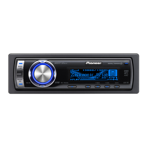
DEH-P6950IB
DEH-P6950IB
This service manual should be used together with the following manual(s):
Model No.
Order No.
CX-3195
CRT3815
For details, refer to "Important Check Points for Good Servicing".
PIONEER CORPORATION
PIONEER ELECTRONICS (USA) INC. P.O. Box 1760, Long Beach, CA 90801-1760, U.S.A.
PIONEER EUROPE NV Haven 1087, Keetberglaan 1, 9120 Melsele, Belgium
PIONEER ELECTRONICS ASIACENTRE PTE. LTD. 253 Alexandra Road, #04-01, Singapore 159936
PIONEER CORPORATION 2006
Mech.Module
S10.5COMP2
CD Mech. Module : Circuit Descriptions, Mech. Descriptions, Disassembly
4-1, Meguro 1-chome, Meguro-ku, Tokyo 153-8654, Japan
DEH-P6950IB/XN/ES
/XN/ES1
Remarks
ORDER NO.
CRT3853
/XN/ES
K-ZZU. DEC. 2006 Printed in Japan
Advertisement
Table of Contents

Related Manuals for Pioneer DEH-P6950IB/XN/ES


Summary of Contents for Pioneer DEH-P6950IB/XN/ES
- Page 1 PIONEER CORPORATION 4-1, Meguro 1-chome, Meguro-ku, Tokyo 153-8654, Japan PIONEER ELECTRONICS (USA) INC. P.O. Box 1760, Long Beach, CA 90801-1760, U.S.A. PIONEER EUROPE NV Haven 1087, Keetberglaan 1, 9120 Melsele, Belgium PIONEER ELECTRONICS ASIACENTRE PTE. LTD. 253 Alexandra Road, #04-01, Singapore 159936 PIONEER CORPORATION 2006 K-ZZU.
-
Page 2: Safety Information
(shorting-solder) by referring to "the DISASSEMBLY". 4. After replacing the pickup unit, be sure to check the grating. 5. Be careful in handling ICs. Some ICs such as MOS type are so fragile that they can be damaged by electrostatic induction. DEH-P6950IB/XN/ES... - Page 3 To protect products from damages or failures during transit, the shipping mode should be set or the shipping screws should be installed before shipment. Please be sure to follow this method especially if it is specified in this manual. DEH-P6950IB/XN/ES...
-
Page 4: Table Of Contents
6.5 SYSTEM MICROCOMPUTER TEST PROGRAM ................... 50 7. GENERAL INFORMATION ..........................51 7.1 DIAGNOSIS ............................. 51 7.1.1 DISASSEMBLY ............................. 51 7.1.2 CONNECTOR FUNCTION DESCRIPTION ..................54 7.2 IC ................................55 7.3 OPERATIONAL FLOW CHART ....................... 65 8. OPERATIONS ..............................66 DEH-P6950IB/XN/ES... -
Page 5: Specifications
1. SPECIFICATIONS Backup current ....5 mA or less DEH-P6950IB/XN/ES... -
Page 6: Exploded Views And Parts List
• Screw adjacent to mark on the product are used for disassembly. • For the applying amount of lubricants or glue, follow the instructions in this manual. (In the case of no amount instructions,apply as you think it appropriate.) 2.1 PACKING DEH-P6950IB/XN/ES... - Page 7 Protector XHP7017 Accessory Assy CEA6708 Case Assy XXA7417 Polyethylene Bag CEG1160 ••••• (2) CONTRAST TABLE DEH-P6950IB/XN/ES and DEH-P6950IB/XN/ES1 are constructed the same except for the following: Mark Description DEH-P6950IB/XN/ES DEH-P6950IB/XN/ES1 Warranty Card Not used CRY1250 Service Network Not used CRY1251...
-
Page 8: Exterior
2.2 EXTERIOR 56 62 DEH-P6950IB/XN/ES... - Page 9 XXA7520 FM/AM Tuner Unit CWE1952 Screw BPZ20P080FTB IC(IC301) PAL007C Button XAC7149 Sub Spring Assy XXA7363 Button XAC7156 Spring XBH7001 Cover XNS7180 Lighting Conductor XNV7035 Connector(CN1801) CKS5207 Connector(CN1802) CKS5545 Double side Tape CNM8673 OEL Unit MXS8231 Holder XNC7009 Holder XNV7029 DEH-P6950IB/XN/ES...
-
Page 10: Cd Mechanism Module
2.3 CD MECHANISM MODULE DEH-P6950IB/XN/ES... - Page 11 Bracket CND2583 CND2584 Lever CND2585 CND2586 Bracket CND2587 CND2588 Lever CND2589 Holder CNV7201 Gear CNV7207 Gear CNV7208 Gear CNV7209 Gear CNV7210 Gear CNV7211 Gear CNV7212 Rack CNV7214 CNV7216 Roller CNV7218 Gear CNV7219 Guide CNV7361 Gear CNV7595 Guide CNV7799 CNV7805 DEH-P6950IB/XN/ES...
-
Page 12: Block Diagram And Schematic Diagram
LCOM CONT CONT /PUEN RESET /RESET /RESET CDRST(RST2) SWVDD 12EJ Q832 BRST,BRXEN,BSRQ BRST,BRXEN,BSRQ,BDATA,BSCK BDATA,BSCK DSCSNS VD 7.5V REGULATOR DPDT Q650 HOME B.UP KYDT Q651 S904 S905 S901 12EJ HOME S903 DSCSNS VDCONT CSENS VDSENS DETACH SENSE SW S802 DSENS DEH-P6950IB/XN/ES... - Page 13 GP1UX31RK KD0-2,KS0-2 OEL UNIT REMOTE CONTROL Q832 SENSOR DPDT DPDT KEY/OEL CONTROLLER DPDT X1841 CN1802 IC1841 KYDT KYDT 16.000MHz XOUT KYDT PEG272A 10,11 LS,CKD,OELD,D_SEL OEL+B OEL+B CSENS 5.1V CSENS DETACH SENSE SW CN1951 Q1881 S802 CN1950 12V REGULATOR Q1882 DEH-P6950IB/XN/ES...
-
Page 14: Overall Connection Diagram(Guide Page)
Therefore, when replacing, be sure to use parts of Ex. *Resistors identical designation. Code Practical value 12k ohms 10k ohms *Capacitors Code Practical value 0.01uF 101/10 100uF/10V DEH-P6950IB/XN/ES... - Page 15 L CH WOOFER R CH FRONT L CH > FRONT R CH REAR L CH FM,AM:-0.9 dBs IPBUS:14.3 dBs REAR CD:14.7 dBs R CH AUX1/IPOD:13.3 dBs 600uH SYSTEM CONTROLLER > CEK1208 FM,AM:21.1 dBs IPBUS:36.3 dBs CD:36.7 dBs AUX1/IPOD:35.3 dBs DEH-P6950IB/XN/ES...
- Page 16 DEH-P6950IB/XN/ES...
- Page 17 DEH-P6950IB/XN/ES...
- Page 18 DEH-P6950IB/XN/ES...
- Page 19 DEH-P6950IB/XN/ES...
-
Page 20: Keyboard Unit
3.3 KEYBOARD UNIT CN1951 MULTI-CONTROL DEH-P6950IB/XN/ES... - Page 21 KEYBOARD UNIT PD8168A OEL UNIT DEH-P6950IB/XN/ES...
-
Page 22: Cd Mechanism Module(Guide Page)
3.4 CD MECHANISM MODULE(GUIDE PAGE) PICKUP UNIT(P10.5)(SERVICE) SWITCHES: CD CORE UNIT(S10.5COMP2) S901:HOME SWITCH..ON-OFF S903:DSCSNS SWITCH..ON-OFF S904:12EJ SWITCH.....ON-OFF S905:8EJ SWITCH....ON-OFF The underlined indicates the switch position. M1 CXC7134 SPINDLE MOTOR M2 CXC4026 LOADING/CARRIAGE MOTOR CD DRIVER DEH-P6950IB/XN/ES... - Page 23 CD CORE UNIT(S10.5COMP2) SIGNAL LINE FOCUS SERVO LINE TRACKING SERVO LINE CARRIAGE SERVO LINE SPINDLE SERVO LINE CN651 & DEH-P6950IB/XN/ES...
- Page 24 DEH-P6950IB/XN/ES...
- Page 25 DEH-P6950IB/XN/ES...
- Page 26 DEH-P6950IB/XN/ES...
- Page 27 DEH-P6950IB/XN/ES...
- Page 28 200 ms/div 500 mV/div 2 ms/div 1 V/div %RFAGC 500 mV/div 500 mV/div 500 mV/div 9TIN 500 mV/div Focus Search waveform Track Open waveform 1 Track Jump waveform Ref.: Ref.: Ref.: REFO REFO REFO Mode: Mode: Mode: TEST TEST TEST DEH-P6950IB/XN/ES...
- Page 29 4LOEJ 312SNS 5 V/div 5 V/div 1 V/div 4LOEJ 0FIN 5 V/div 1 V/div Black dot(800 μm) during play 12 cm CD Eject operation 8 cm CD Eject operation Ref.: Ref.: Ref.: REFO Mode: Mode: Mode: Normal Normal Normal DEH-P6950IB/XN/ES...
-
Page 30: Pcb Connection Diagram
AUX JACK For further information for WIRED REMOTE INPUT respective destinations, be sure to check with the schematic dia- CORD ASSY gram. 2.Viewpoint of PCB diagrams IP-BUS INPUT Capacitor Connector SIDE A SIDE B P.C.Board Chip Part DSENS FRONT DEH-P6950IB/XN/ES... - Page 31 Pod CONNECTOR SIDE A REAR OUTPUT FRONT OUTPUT ANTENNA JACK SUBWOOFER OUTPUT CN352 TESTIN CN1950 CN701 FRONT DEH-P6950IB/XN/ES...
- Page 32 TUNER AMP UNIT >FU 352 (B,128,136) Fuse 3 A CEK1286 DEH-P6950IB/XN/ES...
- Page 33 SIDE B DEH-P6950IB/XN/ES...
-
Page 34: Keyboard Unit
4.2 KEYBOARD UNIT KEYBOARD UNIT KEYBOARD UNIT SIDE A SIDE B CN1951 OEL UNIT MULTI-CONTROL DEH-P6950IB/XN/ES... -
Page 35: Panel Unit
4.3 PANEL UNIT SIDE A PANEL UNIT CN1801 EJECT SIDE B PANEL UNIT CN801 DEH-P6950IB/XN/ES... -
Page 36: Cd Core Unit(S10.5Comp2)
4.4 CD CORE UNIT(S10.5COMP2) CD CORE UNIT(S10.5COMP2) SIDE A CN651 PICKUP UNIT(P10.5)(SERVICE) LOADING /CARRIAGE MOTOR SPINDLE MOTOR DEH-P6950IB/XN/ES... - Page 37 CD CORE UNIT(S10.5COMP2) SIDE B DEH-P6950IB/XN/ES...
-
Page 38: Electrical Parts List
Q 102 (B,37,104) Transistor RT1N141M-11 D 804 (B,121,34) Diode MC2848-11 Q 201 (A,48,75) Transistor 2SC4081 D 805 (B,109,31) Diode MC2846-11 Q 202 (A,55,76) Transistor UMD2N D 821 (A,78,14) Diode HZS9L(B2) Q 301 (A,145,92) Transistor RT1N241M Q 351 (A,138,129) Transistor RT3C99M DEH-P6950IB/XN/ES... - Page 39 R 209 (A,109,74) RS1/16S221J R 645 (A,85,69) RS1/16S221J R 210 (A,72,96) RS1/16S221J R 646 (B,71,36) RS1/16S221J R 212 (A,52,75) RS1/16S152J R 647 (A,71,35) RS1/16S221J R 213 (A,73,93) RAB4C102J R 649 (B,71,34) RS1/16S104J R 301 (A,146,89) RS1/16S103J R 651 (A,18,64) RD1/4PU561J DEH-P6950IB/XN/ES...
- Page 40 C 220 (A,69,99) CEJQ4R7M35 C 221 (A,73,103) CEJQ4R7M35 R 850 (A,28,37) RD1/4PU681J C 222 (A,77,103) CEJQ4R7M35 R 852 (A,33,26) RS1/16S1R0J R 857 (B,38,25) RS1/16S391J C 223 (A,83,103) CEJQ4R7M35 R 858 (A,38,29) RD1/4PU272J C 224 (A,90,103) CEJQ4R7M35 R 859 (B,38,27) RS1/16S391J DEH-P6950IB/XN/ES...
- Page 41 C 702 (A,120,33) CKSRYB473K50 D 1822 (A,40,144) LED SML412BC5T(NP) C 703 (A,117,125) CKSYB475K16 C 705 (A,136,71) CKSRYB105K10 D 1831 (B,26,50) Diode 1SS355 L 1831 (A,29,62) Inductor CTF1617 C 706 (A,133,71) CKSRYB105K10 L 1881 (A,23,130) Inductor CTF1617 C 708 (B,140,87) CKSRYB103K50 DEH-P6950IB/XN/ES...
- Page 42 R 1855 (A,29,69) RS1/16S101J R 101 (B,60,73) RS1/10SR2R4J R 1856 (A,26,69) RS1/16S101J R 102 (B,59,71) RS1/10SR2R4J R 1857 (B,18,58) RS1/16S101J R 103 (B,60,71) RS1/10SR2R7J R 1858 (B,19,55) RS1/16S473J R 104 (B,52,69) RS1/16SS222J R 105 (B,41,57) RS1/16SS102J R 1859 (B,26,55) RS1/16S154J DEH-P6950IB/XN/ES...
- Page 43 C 217 (A,46,51) CKSSYB104K10 C 218 (A,49,51) CKSSYB473K10 C 219 (A,45,53) CKSSYB104K10 C 220 (A,46,53) CKSSYB182K50 C 221 (A,44,53) CKSSYB104K10 C 222 (B,43,53) CCSSCH560J50 C 223 (B,45,53) CCSSCH4R0C50 C 224 (A,43,55) CKSSYB104K10 C 226 (A,40,58) CCSSCH680J50 C 227 (A,40,60) CCSSCH470J50 DEH-P6950IB/XN/ES...
-
Page 44: Adjustment
1 k ohms in series. • The load and eject operation is not guarantied with the mechanism upside down. If the mechanism is blocked due to mistaken eject operation, reset the product or turn off and on the ACC to restore it. DEH-P6950IB/XN/ES... - Page 45 • When the power is turned on/off the jump mode is reset to the Single TR (91) while the gain of the RFAMP is reset to 0 dB. At the same time all the self-adjusting values shall return to the default setting. DEH-P6950IB/XN/ES...
-
Page 46: Checking The Grating After Changing The Pickup Unit
Because of eccentricity in the disc and a slight misalignment of the clamping center the grating waveform may be seen to "wobble" ( the phase difference changes as the disc rotates). The angle specified above indicates the average angle. • Hint Reloading the disc changes the clamp position and may decrease the "wobble". DEH-P6950IB/XN/ES... - Page 47 Ech → Xch 20 mV/div, AC Grating waveform Fch → Ych 20 mV/div, AC 0° 30° 45° 60° 75° 90° DEH-P6950IB/XN/ES...
-
Page 48: Error Mode
Remarks: Mechanical errors are not displayed (because a CD is turned off in these errors). Unreadable TOC does not constitute an error. An intended operation continues in this case. Upper digits of an error code are subdivided as shown below: 1x: Setup relevant errors, 3x: Search relevant errors, Ax: Other errors. DEH-P6950IB/XN/ES... -
Page 49: Ipod Test Mode
[Features of this test mode] Enables switching at any time to the iPod source Disables communication with iPod Disables indication of logos (Pioneer) on iPod Functions regardless of connection of the iPod body to H/U [How to shift to test mode] The following describes how to enter and display the test mode. -
Page 50: System Microcomputer Test Program
The frequency of the clock signal is 625 kHz that is one 32th of the fundamental frequency. The clock signal should be 625 kHz(±25 Hz). If the clock signal is out of the range, the X'tal (X601) should be replaced with new one. DEH-P6950IB/XN/ES... -
Page 51: General Information
Remove the two screws and then remove the Grille Assy. Fig.1 Grille Assy Removing the Tuner Amp Unit (Fig.2) Remove the screw. Remove the three screws. Straighten the tabs at four locations indicated and then remove the Tuner Amp Unit. Tuner Amp Unit Fig.2 DEH-P6950IB/XN/ES... - Page 52 Upper Frame. 3. While lifting the Carriage Mechanism, remove it from the three Dampers. Caution: When assembling, be sure to apply some alcohol to the Dampers and assemble the mechanism in a clamped state. Damper Damper Carriage Mechanism Lower Frame DEH-P6950IB/XN/ES...
- Page 53 Assemble the sub unit side of the Pickup, taking the plate (Chassis) in-between. When treating the leads of the Load Carriage Motor Assy, do not make them loose over the Feed Screw. Poly Washer Change Arm Pickup Lock Arm Inner Holder Feed Screw Planet Gear Pickup Rack Chassis Pickup DEH-P6950IB/XN/ES...
-
Page 54: Connector Function Description
7.1.2 CONNECTOR FUNCTION DESCRIPTION DEH-P6950IB/XN/ES... - Page 55 7.2 IC NJM2794V OUT1 IN1+ IN1- OUT1 IN1+ IN1- VREF Vref IN2- IN2+ OUT2 IN2- OUT2 IN2+ PML016B - Pin Layout DEH-P6950IB/XN/ES...
- Page 56 - Block Diagram DEH-P6950IB/XN/ES...
- Page 57 PAL007C TC4066BFT IN/OUT1 1 14 VDD OUT/IN1 2 13 CONT1 OUT/IN2 3 12 CONT4 IN/OUT2 4 11 IN/OUT4 CONT2 5 10 OUT/IN4 9 OUT/IN3 CONT3 6 VSS 7 8 IN/OUT3 DEH-P6950IB/XN/ES...
- Page 58 EVOL : Source select SW(iPod) IPODON Not used 53-56 EVOL : Mute EMUTE Level indicator clock output SACLK Not used Power supply input VCC2 Not used Communication mode(UART) notification output psensg Connection sense input Power supply control output PPOWER DEH-P6950IB/XN/ES...
- Page 59 P-BUS : Input/Chip test program data input BSI/TESTDI P-BUS : Output/Chip test program data output BSO/TESTDO BSCK/TESTCLK P-BUS : Clock output/Chip test program data clock PEG274A Format Meaning CMOS Nch open drain PE5547A Format Meaning CMOS Nch open drain DEH-P6950IB/XN/ES...
- Page 60 Power supply for the crystal oscillator X.VDD Power supply for DAC DA.VDD Output of audio for the left channel LOUT Ground for DAC DA.GND Connected to the capacitor for band gap REGC Ground for DAC DA.GND ROUT Output of audio for the right channel DEH-P6950IB/XN/ES...
- Page 61 Output of reference voltage REFOUT Reversal input of FE Output of FE FE,TE A/D converter input ADCIN Reversal input of TE Output of TE Output of LD Input of PD Power supply for servo ADC AD.VDD Ground for servo ADC AD.GND DEH-P6950IB/XN/ES...
- Page 62 Image ROM : Address bus 9 bit Power supply input VCC2 Image ROM : Address bus 8 bit VSS2 Image ROM : Address bus 7 bit Image ROM : Address bus 6 bit Image ROM : Address bus 5 bit DEH-P6950IB/XN/ES...
- Page 63 Key data 3(Not used) kd@,! Key data 2,1 92,93 Analog GND AVSS Key data 0 Reference voltage input VREF Analog power supply input AVCC Terminal for Dimmer control Not used 99,100 PEG272A Format Meaning CMOS Nch open drain PD8168A(P5900IB) DEH-P6950IB/XN/ES...
- Page 64 22 AUDIOGND audio ground Ground of audio block 23 L ch O L channel output FM stereo “L-ch” signal output or AM audio output 24 R ch O R channel output FM stereo “R-ch” signal output or AM audio output DEH-P6950IB/XN/ES...
-
Page 65: Operational Flow Chart
In case of the above signal, the communication Source keys with Grille microcomputer may fail. operative If the time interval is not 300 msec, the oscillator may be defective. Source ON SYSPW←H Pin 1 Completes power-on operation. (After that, proceed to each source operation.) DEH-P6950IB/XN/ES... -
Page 66: Operations
8. OPERATIONS DEH-P6950IB/XN/ES... - Page 67 DEH-P6950IB/XN/ES...
- Page 68 CXX1645 CXX1644 XXX7020 DEH-P6950IB/XN/ES...
- Page 69 - Connection Diagram DEH-P6950IB/XN/ES...
- Page 70 CD Mechanism Module Before shipping out the product, be sure to clean the following portions by using the prescribed cleaning tools: Portions to be cleaned Cleaning tools CD pickup lenses Cleaning liquid : GEM1004 Cleaning paper : GED-008 g p p DEH-P6950IB/XN/ES...