Sony MDX-62 Service Manual
Hide thumbs
Also See for MDX-62:
- Operating instructions manual (24 pages) ,
- Operating instructions (2 pages)
Table of Contents
Advertisement
Quick Links
SERVICE MANUAL
• Electrical adjustment of this set is automatically performed.
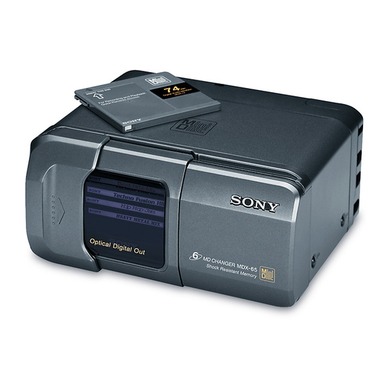
SPECIFICATIONS
System
Mini disc digital audio system
Laser Diode Properties
Material: GaAlAs
Wavelength: 780 nm
Emission Duration: Continuous
Laser output Power: Less than
44.6 µW*
* This output is the value measured at a distance of
200 mm from the objective lens surface on the
Optical Pick-up Block.
Frequency response
10 – 20,000 Hz
Wow and flutter Below measurable limit
Signal-to-noise ratio
95 dB
Outputs
Bus control output (8 PIN)
Analog audio output (RCA PIN)
Current drain
300 mA (MD playback)
600 mA (during loading or ejecting a
disc)
Approx. 176 × 83.5 × 130 mm
Dimensions
(7 × 3
× 5
/
/
in.) (w/h/d) not incl.
3
1
8
8
projecting parts and controls
Mass
Approx. 1.1 kg (2 lb. 7 oz.)
Power requirement
12 V DC car battery (negative
ground)
Supplied accessories
Mounting hardware (1 set)
Bus cable 5.5 m (1)
RCA pin cord 5.5 m (1)
• U.S. and foreign patents licensed from Dolby
Laboratories Licensing Corporation.
• Design and specifications subject to change without
notice.
MICROFILM
MDX-62
Model Name Using Similar Mechanism
Mini Disc Mechanism Type
Optical Pick-up Name
FEATURES
• Sony BUS system compatible with mobile MD
changers.
• Direct-in system for inserting and removing
MDs easily.
• No waiting time to change discs in continuous
play.
• The MD changer compartment has a built in light
for easy use even in the dark.
• 1 bit Digital/Analog converter for high quality
sound reproduction.
• The Digital D-BASS function* creates an even
sharper and more powerful sound than Analog
D-BASS.
* This unit supports Digital D-BASS function if the
master unit also has Digital D-BASS function.
– 1 –
US Model
Canadian Model
AEP Model
UK Model
E Model
NEW
MG-798K-133
KMS-241A/J2N
MINIDISC CHANGER
Advertisement
Table of Contents

Related Manuals for Sony MDX-62


Summary of Contents for Sony MDX-62
- Page 1 MG-798K-133 Optical Pick-up Name KMS-241A/J2N SPECIFICATIONS FEATURES System Mini disc digital audio system • Sony BUS system compatible with mobile MD Laser Diode Properties changers. Material: GaAlAs • Direct-in system for inserting and removing Wavelength: 780 nm MDs easily. Emission Duration: Continuous •...
-
Page 2: Table Of Contents
LES COMPOSANTS IDENTIFIÉS PAR UNE MARQUE ! SUR LES DIAGRAMMES SCHÉMATIQUES ET LA LISTE DES PIÈCES SONT CRITIQUES POUR LA SÉCURITÉ DE FONCTIONNEMENT. NE REMPLACER CES COMPOSANTS QUE PAR DES PIÈCES SONY DONT LES NUMÉROS SONT DONNÉS DANS CE MANUEL OU DANS LES SUPPLÉMENTS PUBLIÉS PAR SONY. -
Page 3: Service Note
For key control, the this set is controlled through serial communication with a master unit (car audio player, TV tuner or source selector compatible with the Sony BUS system.) To service the this set, the set should be connected as given below:... -
Page 4: General
SECTION 2 GENERAL This section extracted from US, Canadian, E model’s instruction manual. – 4 – – 5 –... - Page 5 – 6 – – 7 –...
-
Page 6: Disassembly
SECTION 3 DISASSEMBLY Note : Follow the disassembly procedure in the numerical order given. 3-1. PANEL (REAR) ASSY 1 BVTT 2.6x6 2 BVTT 2.6x6 3 PTT 2.6x8 5 CN901 4 panel (rear) assy 3-2. CASE (UPPER) 3 case (upper) 1 BVTT 2.6x6 2 BVTT 2.6x6 –... -
Page 7: Panel (Front) Assy
3-3. PANEL (FRONT) ASSY 3 panel (front) assy 1 claw 4 CN620 2 claw 3-4. MD BLOCK 4 tension spring (FL) 6 MD block 1 damper (798) 2 damper (798) 5 tension spring (FL) 3 tension spring (FL) – 9 –... -
Page 8: Main Board
3-5. MAIN BOARD 3 escutcheon 6 chassis (front) 7 collar (EHS) 0 CN600 !¡ CN601 !£ CN603 !¢ CN701 !™ CN500 5 lead stopper !∞ CN700 4 screws (M1.7) 9 CN602 2 screws (M1.7) 1 cushion !¶ special flat screws 8 sheet (MAIN PC board) (1.7x3) !•... -
Page 9: Servo Board
3-7. SERVO BOARD 3 CN100 2 screws (M1.7x2.2) 5 CN300 7 SERVO board 1 CN200 6 Unsolder the 4 CN400 motor lead wires. 3-8. OPTICAL PICK-UP 1 screws (K1.7x3.5) 2 optical pick-up – 11 –... -
Page 10: Note On Assembly For The Chassis (Op) Block
3-9. NOTE ON ASSEMBLY FOR THE CHASSIS (OP) BLOCK Note : Follow the disassembly procedure in the numerical order given. 2 bearing (ELV) 3 chassis (OP) block 5 chassis (bottom) assy 1 Turn the three feed screw (ELV) assy fully in 6 precision screw the direction of arrows A . -
Page 11: Diagrams
SECTION 4 DIAGRAMS 4-1. IC PIN DESCRIPTIONS • IC100 CXA2523AR (RF AMP) Pin No. Pin Name Pin Description I-V converted RF signal input (I) from detector of optical pick-up. I-V converted RF signal input (J) from detector of optical pick-up. Center voltage (+1.65 V) generation output 4 –... - Page 12 Serial data input for SONY BUS. UNISO Serial data output for SONY BUS. UNI CKI Serial clock input for SONY BUS. LINKOFF Link control signal output for SONY BUS. (“H” : Link OFF) — Not used. — Not used. 51, 52...
- Page 13 Pin No. Pin Name Pin Description — Not used. EE CS Chip select output to EEPROM. (Not used in this set.) EE CKO Serial clock output to EEPROM. (Not used in this set.) EE SIO Data input from/output to EEPROM. (Not used in this set.) SENS Internal status input from CXD2652AR (IC200).
-
Page 14: Circuit Boards Location
4-2. CIRCUIT BOARDS LOCATION SENSOR board POWER board MAIN board SERVO board LAMP board – 16 –... - Page 22 • Waveforms – Servo Section – 1 IC100 4 (A) PLAY MODE 5 IC100 #• (RF) PLAY MODE 9 IC200 @§ (XBCK) 200 mV/DIV, 10 µ sec/DIV 500 mV/DIV, 1 µ sec/DIV 3.2 Vp-p Approx. Approx. 1.1 Vp-p 150 mVp-p 354 ns 2 IC100 8 (E) PLAY MODE 6 IC100 #¢, IC200 ^∞...
- Page 23 – Main Section – 1 IC600 !º (X2) 5 IC500 1 (XT1) 3.2 Vp-p 2.7 Vp-p 89 ns 71 ns 2 IC600 !¢ (XT1) 2.6 Vp-p 30.4 µs 3 IC500 4 (LRCK) 2.8 Vp-p 22.7 µs 4 IC500 6 (BCK) 2.8 Vp-p 354 ns –...
- Page 24 • IC Block Diagrams – Servo Section – IC100 CXA2523AR 43 42 USROP – RF AGC – USRC RFA1 BPF3T RFA2 RFA3 PEAK3T – HLPT –1 – – –2 – OFST PTGR TEMP PEAK – –2 – 36 BOTM BOTTOM –...
- Page 25 IC200 CXD2652AR 100 99 98 97 96 95 94 93 92 91 90 89 88 87 86 85 84 83 82 81 80 79 78 77 76 75 AUX2 SPINDLE GENERATOR SERVO 74 TE MNT0 73 SE MNT1 MONITOR EACH 72 AVSS CONTROL BLOCK...
- Page 26 – Main Section – IC500 PCM1717E-ST2 IC520 TC7W74FU (TE12R) CONTROL CLKO DGND INPUT MUTE INTERFACE LRCIN MODE CONTROL RSTB DIGITAL FORMAT FILTER BCKIN NOISE SHAPER ZERO 5 LEVEL 5 LEVEL LOWPASS LOWPASS FILTER FILTER CMOS CMOS D/C R D/C L VOUTR VOUTL AGND...
-
Page 27: Exploded Views
SECTION 5 EXPLODED VIEWS NOTE: • The mechanical parts with no reference • Color Indication of Appearance Parts The components identified by number in the exploded views are not supplied. Example : mark ! or dotted line with mark. • Items marked “*” are not stocked since KNOB, BALANCE (WHITE) ... -
Page 28: Main Board Section
5-2. MAIN BOARD SECTION MG-798K-133 not supplied Ref. No. Part No. Description Remark Ref. No. Part No. Description Remark * 51 3-931-149-02 SHEET (MAIN PC BOARD) 3-931-699-01 CUSHION (ROLL H) * 52 A-3294-415-A MAIN BOARD, COMPLETE * 59 3-931-025-01 SHEET (MECHANISM DECK) 1-776-474-11 CABLE, FLAT 7P 3-931-698-01 CUSHION (ROLL L) 3-909-412-01 SCREW (+P) (1.7X2) (TYPE 3) -
Page 29: Md Section (1)
5-3. MD SECTION (1) (MG-798K-133) S903 S902 M903 M904 Ref. No. Part No. Description Remark Ref. No. Part No. Description Remark 3-317-552-71 SCREW (M1.7) 3-377-719-11 WASHER, POLYETHYLENE 3-930-314-01 ESCUTCHEON 3-930-317-01 GEAR (LD) 3-930-319-01 BUTTON (STOP) * 114 X-3374-670-1 CHASSIS (BOTTOM) ASSY * 104 3-930-320-01 CHASSIS (FRONT) 3-930-313-01 GEAR (ELVC) -
Page 30: Md Section (2)
5-4. MD SECTION (2) (MG-798K-133) Ref. No. Part No. Description Remark Ref. No. Part No. Description Remark * 151 X-3371-209-3 CHASSIS (TOP) ASSY 3-930-350-01 SPRING (EJ), TORSION * 152 3-020-388-01 GUIDE (HOLDER 2) X-3371-216-1 HOLDER (CADDIE) ASSY 3-930-318-01 BUTTON (EJECT) (6 1) 3-930-352-01 SPRING (D LOCK), TENSION 3-930-318-11 BUTTON (EJECT) (6 2) * 164... - Page 31 5-5. MD SECTION (3) (MG-798K-133) RV901 M901 M902 S901 The components identified by Les composants identifiés par une mark ! or dotted line with mark. marque ! sont critiques pour la ! are critical for safety. sécurité. Replace only with part number Ne les remplacer que par une piéce specified.
-
Page 32: Electrical Parts List
SECTION 6 LAMP MAIN ELECTRICAL PARTS LIST NOTE: • Due to standardization, replacements in • Items marked “*” are not stocked since The components identified by the parts list may be different from the they are seldom required for routine service. mark ! or dotted line with mark. - Page 33 MAIN POWER Ref. No. Part No. Description Remark Ref. No. Part No. Description Remark IC700 8-759-823-87 IC LB1638M R626 1-216-825-11 METAL CHIP 2.2K 1/16W IC701 8-759-823-87 IC LB1638M R627 1-216-821-11 METAL CHIP 1/16W R628 1-216-825-11 METAL CHIP 2.2K 1/16W < RESISTOR > R800 1-216-815-11 METAL CHIP 1/16W...
- Page 34 POWER SENSOR Ref. No. Part No. Description Remark Ref. No. Part No. Description Remark C952 1-110-454-11 ELECT CHIP 10uF < IC LINK > C970 1-163-133-00 CERAMIC CHIP 470PF C971 1-163-986-00 CERAMIC CHIP 0.027uF PS900 1-533-397-11 LINK, CHIP IC (ICP-S2.3) (2.3A) C973 1-164-004-11 CERAMIC CHIP 0.1uF...
- Page 35 SERVO Ref. No. Part No. Description Remark Ref. No. Part No. Description Remark A-3294-337-A SERVO BOARD, COMPLETE < DIODE > ********************** D300 8-719-988-62 DIODE 1SS355 < CAPACITOR > < FERRITE BEAD > C100 1-107-685-11 TANTAL. CHIP 15uF 6.3V C101 1-135-201-11 TANTALUM CHIP 10uF FB200 1-414-594-11 INDUCTOR, FERRITE BEAD C102...
- Page 36 SERVO Ref. No. Part No. Description Remark Ref. No. Part No. Description Remark < NETWORK RESISTOR > PARTS FOR INSTALLATION AND CONNECTIONS *************************************** RB200 1-233-576-11 RES, CHIP NETWORK 100 RB300 1-233-600-11 RES, CHIP NETWORK 2.2 3-930-163-01 BASE (FITTING) RB301 1-233-600-11 RES, CHIP NETWORK 2.2 X-3371-178-1 BRACKET ASSY 3-930-166-01 CUSHION (FITTING) <...
- Page 37 MDX-62 Sony Corporation 98A0482-1 9-925-786-11 Personal & Mobile Communication Company Printed in Japan C1998. 1 – 50 – Published by Quality Assurance Dept.