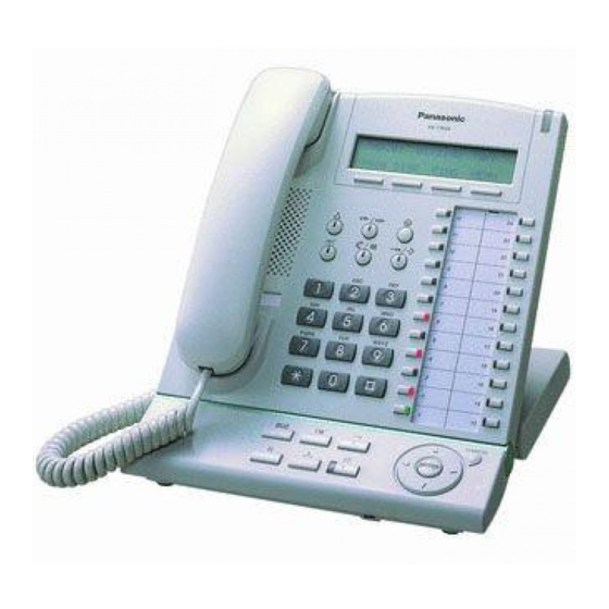
Panasonic KX-T7630 Service Manual
Digital proprietary telephone
Hide thumbs
Also See for KX-T7630:
- Operating instructions manual (25 pages) ,
- Operator user manual (18 pages) ,
- Quick reference manual (17 pages)
Table of Contents
Advertisement
IMPORTANT INFORMATION ABOUT LEAD FREE, (PbF),
SOLDERING
If lead free solder was used in the manufacture of this product the printed circuit boards will be
marked PbF.
Standard leaded, (Pb), solder can be used as usual on boards without the PbF mark.
ORDER NO. KMS0303671C3
Digital Proprietary Telephone
1
KX-T7630
(for Australia)
Advertisement
Table of Contents

Related Manuals for Panasonic KX-T7630


Summary of Contents for Panasonic KX-T7630
- Page 1 ORDER NO. KMS0303671C3 Digital Proprietary Telephone KX-T7630 (for Australia) IMPORTANT INFORMATION ABOUT LEAD FREE, (PbF), SOLDERING If lead free solder was used in the manufacture of this product the printed circuit boards will be marked PbF. Standard leaded, (Pb), solder can be used as usual on boards without the PbF mark.
-
Page 2: About Lead Free Solder (Pbf: Pb Free)
When this mark does appear please read and follow the special instructions described in this manual on the use of PbF and how it might be permissible to use Pb solder during service and repair work. 1. ABOUT LEAD FREE SOLDER (PbF: Pb free) Note: In the information below, Pb, the symbol for lead in the periodic table of elements, will refer to standard solder or solder that contains lead. -
Page 3: For Service Technicians
(Sn+Ag+Cu), you can also use Tin and Copper, (Sn+Cu), or Tin, Zinc, and Bismuth, (Sn+Zn+Bi). Please check the manufac turer’s specific instructions for the melting points of their products and any precautions for using their product with other materials. The following lead free (PbF) solder wire sizes are recommended for service of this product: 0.3mm, 0.6mm and 1.0mm. - Page 5 5. CONNECTION Caution: Consult your dealer for more details about XDP. 6. DISASSEMBLY INSTRUCTIONS 1. Remove 9 Screws (A). 2. Remove the Bottom Cabinet.
-
Page 6: How To Replace A Flat Package Ic
3. Remove the P. C. Board from the Top Cabinet. 7. HOW TO REPLACE A FLAT PACKAGE IC 7.1. PREPARATION - PbF (: Pb free) Solder - Soldering Iron Tip Temperature of 700°F ± 20°F (370°C ± 10°C) Note: We recommend a 30 to 40 Watt soldering iron. An expert may be able to use a 60 to 80 Watt iron where someone with less experience could overheat and damage the PCB foil. -
Page 7: Troubleshooting Guide
Be certain each pin is located over the correct pad on the PCB. 2. Apply flux to all of the pins on the IC. 3. Being careful to not unsolder the tack points, slide the soldering iron along the tips of the pins while feeding enough solder to the tip so that it flows under the pins as they are heated. - Page 8 8.1. NO OPERATION Note: Refer to (1)~(5) of WAVEFORM () for waveform. 8.2. LCD DOES NOT OPERATION...
- Page 9 Note: Refer to (6) of WAVEFORM () for waveform. 8.3. HANDSET DOES NOT WORK Receive Send...
- Page 10 Note: Refer to (7)~(8) of WAVEFORM () for waveform. 8.4. HEADSET DOES NOT WORK Receive Send Note:...
-
Page 11: Speaker-Phone Trouble
Refer to (7)~(8) of WAVEFORM () for waveform. 8.5. SPEAKER-PHONE TROUBLE Receive Send Note: Refer to (7)~(8) of WAVEFORM () for waveform. 8.6. DXDP-DPT DOES NOT WORK... - Page 12 Note: Refer to (9) of WAVEFORM () for waveform. 9. BLOCK DIAGRAM 10. CIRCUIT OPERATIONS 10.1. KEY INPUT CONTROL CIRCUIT The key data is under the matrix control by 19 to 23, 25, 44, 45(KEYOUT) and 28 to 35(KEYIN) of IC3.
-
Page 13: Lcd Circuit
10.2. LCD CIRCUIT LCD data are outputted from pin 57, 58, 59,10 and 12 of IC3 to LCD module. IC8 is an inverter for a charge pump circuit which outputs the voltage necessary for LCD driving. - 4.5V from -1.2V generated at IC8 as a reference to +3.3V of the power supply voltage is pressurized four times in the LCD module and used as LCD driving voltage (approx. - Page 14 Pin 62 of IC3 L KX-T7636 24 digits * 6 lines H KX-T7630/KX- 24 digits * 3 lines T7633 The lighting of the backlight is controlled by Q1. - IC3-pin 56H Q1-ON Backlight ON - IC3-pin 56L Q1-OFF Backlight OFF...
-
Page 15: Led Circuit
10.3. LED CIRCUIT The lighting of the LED is controlled by pin 19 to 28 (Row) and pin 11 to 16 (Colum) of IC5. The LED lights up in a dynamic lighting system. The duty ratio is 1/8(ON time 1.5mS). Only D107 of LED for CO7 lights up in a static lighting system. -
Page 16: Reset Circuit
10.4. RESET CIRCUIT Reset Signal is outputted from IC1 and inputted into IC3 and IC5 at the connection of TEL cord. -
Page 17: Power Supply Circuit
10.5. POWER SUPPLY CIRCUIT This circuit converts the voltage supplied from PBX into the power supply voltage of +3.3V by IC6(Switching Regulator IC). IC10 controls the power supply circuit as below to turn IC6 on in low consumption current at starting up. -
Page 18: Data Communication
10.6. DATA COMMUNICATION Function The data communication circuit serves the following functions: Information exchanger between PBX and proprietary telephone, key input information as well as data for the LED control, LCD control, voice data, etc. This information is continuously exchanged at all times. Circuit Operation The data received from PBX is inputted to the comparator(pin 68) built in IC5 through Pulse Trans T1. - Page 19 10.7. DXDP COMMUNICATION Function This circuit performs the same communication as DXDP-compatible DPT and PBX communication connected with DXDP port. Circuit Operation The data to Slave DPT is outputted from pin 63 and 64 of IC5 and sent by Transistor Q8 and Q9. The data from Slave DPT is inputted to the comparator(pin 61) built in IC5.
-
Page 20: Analog Circuit
10.8. ANALOG CIRCUIT This circuit performs the setting of the call path/vol. adjustment in each call mode by DSP built in IC5. The audio gain of each call is determined by download data from PBX. - IC5 sends each audio data to IC4 by PCM interface. - IC5 receives each audio data from IC4 by PCM interface. - Page 21 PCM data Gain adjustment by DSP of IC5 then sent to PBX. Transmitting signal inputted from headset microphone is controlled by transmission switching SW IC7 as below. IC3-pin 52 H : Headset Call (IC3-pin 52 L : Handset Call) Receiving signal inputted from PBX is Gain adjustment by DSP of IC5 D/A conversion after the input to IC4 in PCM data...
- Page 22 I/O Setting Pull-up Contents of Control Remark Processing Built-in Write signal Built-in Read signal Built-in Chip select input INTN Interrupt output PVSS Ground for DSP PLL PVDD Power supply for DSP PLL DSP PLL adjustment PLLI DSP PLL adjustment PLLO DSP PLL adjustment Digital ground CML5...
- Page 23 I/O Setting Pull-up Contents of Control Remark Processing Channel pulse 2.048MHz serial data output Built-in 2.048MHz serial data input OSYNC 8Khz frame synchronized signal OCK2M 2.048MHz serial clock (Schmitt) OCK4MN 4.096MHz serial clock Optional reset output 1 Optional reset output 2 Codec serial data output Codec serial clock output Digital ground...
- Page 24 I/O Setting Pull-up Contents of Control Remark Processing Digital ground Digital power supply PVRL Reference voltage for comparator Receive data input PVRH Reference voltage for comparator PDX0 Send data output PDX1 Send data output SCANE Built- Scan test enable pin in(down) SCAN Built-...
- Page 25 I/O Setting Pull-up Contents of Control Remark Processing not inuse Connecting to Vcc not inuse Open OSC2 Open OSC1 8 MHz clock from 8.192MHz ASIC TEST not inuse Connecting to Vcc Power terminal +3.3V Reset/ Reset input Low active P20/IRQ4 Built-in OP-Rx-Rdy P21/SCK1...
-
Page 26: Terminal Guide Of Ics, Transistors And Diodes
P51/WKP1 Built-in KEY-IN1 P52/WKP2 Built-in KEY-IN2 P53/WKP3 Built-in KEY-IN3 P54/WKP4 Built-in KEY-IN4 P55/WKP5 Built-in KEY-IN5 P56/WKP6 Built-in KEY-IN6 P57/WKP7 Built-in not in use Built-in Built-in Built-in Built-in Built-in Built-in Built-in Built-in AD0/KEY-OUT6 AD1/KEY-OUT7 SP_AMP OFF H:OFF L:ON MIC switch L: Hand set, H: Head EEPROM CLK Clock output (out) -
Page 27: Cabinet And Electrical Parts Location
13. CABINET AND ELECTRICAL PARTS LOCATION... -
Page 28: Accessories And Packing Materials
14. ACCESSORIES AND PACKING MATERIALS... -
Page 29: Replacement Parts List
15. REPLACEMENT PARTS LIST 1. RTL (Retention Time Limited) Note: The marking (RTL) indicates that the Retention Time is limited for this item. After the discontinuation of this assembly in production, the item will continue to be available for a specific period of time. The retention period of availability is dependent on the type of assembly, and in accordance with the laws governing parts and... -
Page 30: Cabinet And Electrical Parts
product retention. After the end of this period, the assembly will no longer be available. 2. Important safety notice Components identified by mark have special characteristics important for safety. When replacing any of these components, use only manufacture's specified parts. 3. - Page 31 Ref. No. Part No. Part Name & Description Remarks PSKM1094X1 CABINET BODY ABS-HB PSHR1251Z TRANSPARENT PLATE (LARGE) PSGD1061Z TEL. CARD (LARGE) PQHR576Z TRANSPARENT PLATE (SMALL) PQHP532X TEL. CARD (SMALL) PQKE10070Z3 LID, HOOK KNOB ABS-HB PSGP1075Z COVER, LED LENS ABS-HB PSKK1038Z2 LID, SHAFT COVER ABS-HB PSKM1084Z1...
- Page 32 Ref. No. Part No. Part Name & Description Remarks PSJA1082Z CORD, TELEPHONE PSJA1043Z CORD, HANDSET PQJXF0502Z HANDSET PSQX2508Z INSTRUCTION BOOK (QUICK REFERENCE GUIDE) PSZKT7630AL GIFT BOX ASS'Y XZB34X48A05 PROTECTION COVER 15.3. MAIN AND SUB BOARDS PARTS Ref. No. Part No. Part Name &...
- Page 33 Ref. No. Part No. Part Name & Description Remarks D103 PQVDBRPY1204 LED D104 PQVDBRPY1204 LED D105 PQVDBRPY1204 LED D106 PQVDBRPY1204 LED D107 PQVDBRPY1204 LED D108 PQVDBRPY1204 LED D109 PQVDBRPY1204 LED D110 PQVDBRPY1204 LED D111 PQVDBRPY1204 LED D112 PQVDBRPY1204 LED D113 PQVDBRPY1204 LED D114 PQVDBRPY1204 LED...
- Page 34 Ref. No. Part No. Part Name & Description Remarks PFVF1B601ST CERAMIC FILTER PFVF1B601ST CERAMIC FILTER PFVF1B601ST CERAMIC FILTER (COIL) G1A331D00005 COIL (COMPONENT PARTS) D1H81224A010 RESISTOR ARRAY (TRANSFORMER) ETJS13ZA14AB TRANSFORMER (CRYSTAL OSCILLATOR) PSVCC0052C CRYSTAL OSCILLATOR (RESISTORS) ERJ3GEY0R00 ERJ6GEYJ3R3 ERJ3GEYJ105 ERJ3GEYJ105 ERJ3GEYJ105 ERJ3GEYJ105 ERJ3GEYJ471 ERJ3GEYJ473...
- Page 35 Ref. No. Part No. Part Name & Description Remarks ERJ3GEYJ473 ERJ3GEYJ393 ERJ3GEYJ562 5.6k ERJ3GEYJ473 ERJ3GEYJ221 ERJ3GEYJ103 ERJ3GEYJ181 ERJ3GEYJ102 ERJ3GEYJ102 ERJ3GEYJ102 ERJ3GEYJ471 ERJ3GEYJ471 ERJ3GEYJ471 ERJ3GEYJ122 1.2k ERJ3GEYJ122 1.2k ERJ3GEYJ105 ERJ3GEYJ331 ERJ3GEYJ182 1.8k ERJ3GEYJ182 1.8k ERJ3GEYJ822 8.2k ERJ3GEYJ562 5.6k ERJ3GEYJ123 ERJ3GEYJ562 5.6k ERJ3GEYJ682 6.8k ERJ3GEYJ103...
- Page 36 Ref. No. Part No. Part Name & Description Remarks ERJ3GEYJ270 ERJ3GEYJ562 5.6k ERJ3GEYJ180 R100 ERJ3GEYJ330 R101 ERJ3GEYJ100 R102 ERJ3GEYJ223 R103 ERJ3GEYJ681 R104 ERJ3GEYJ270 R105 ERJ3GEYJ270 R106 ERJ3GEYJ270 R107 ERJ3GEY0R00 R108 ERJ3GEYJ121 R109 ERJ3GEYJ473 R110 ERJ3GEYJ473 R111 ERJ3GEYJ473 R116 ERJ3GEYJ153 R117 ERJ3GEYJ102 R118 ERJ3GEYJ105...
- Page 37 Ref. No. Part No. Part Name & Description Remarks ECUV1C104ZFV 0.1 ECUV1C104ZFV 0.1 ECUV1H103KBV 0.01 ECUV1H103KBV 0.01 F2G0J1010014 F3F0G226A029 ECUV1A106ZF ECUV1A106ZF ECUV1A106ZF ECUV1H122KBV 0.0012 ECUV1C104ZFV 0.1 ECUV1H100DCV 10p ECUV1C104KBV 0.1 ECUV1C104KBV 0.1 ECUV1H153KBV 0.015 ECUV1H152KBV 0.0015 ECUV1H820JCV 82p ECUV1H680JCV 68p ECUV1H332KBV 0.0033 ECUV1C104KBV 0.1 PQCUV1C224ZF 0.22...
-
Page 38: For The Schematic Diagram
Ref. No. Part No. Part Name & Description Remarks EEEFK0J101P ECUV1C104ZFV 0.1 ECUV1H101JCV 100p ECUV1H101JCV 100p ECUV1C104ZFV 0.1 PQCUV1C105ZF 1 PQCUV1C105ZF 1 C100 PQCUV1H105JC 1 C101 ECUV1C104ZFV 0.1 C102 PQCUV1C224ZF 0.22 C103 PQCUV1C105ZF 1 C104 PQCUV1H105JC 1 C105 ECUV1H103KBV 0.01 C106 ECUV1E104ZFV 0.1 C107... - Page 39 17. SCHEMATIC DIAGRAM 18. WAVEFORM 19. PRINTED CIRCUIT BOARD (MAIN / SUB BOARDS) 19.1. COMPONENT VIEW 19.2. BOTTOM VIEW Y / KXT7630AL /...
- Page 40 HS2SP MIC2 HS2MIC A3.3V2 C114 R120 C112 R126 8.2K A3.3V C113 R125 270K A3.3V VFR0 VFTP1 R128 VFTP0 C144 GSR0 VREF 1000P TO HANDSET MIC1 R130 VFTN0 A3.3V 220K Z0.01 GST0 MIC3 VFTN1 560K GST1 BCLK GSR1 VFR1 A3.3V SP3+ SCLK 5 VO1 DATA...
- Page 41 (11) (13) (15) (2)(3) (4) (5) (7)(8) (10) (12) (14) (16) (17) (18) D3.3V Z0.01 D3.3V D3.3V C26 Z0.01 Z0.1 Z0.1 VSS2 Z0.1 VSS2 -1.2V Z2.2 VOUT 1 X1 VOUT D3.3V 2 X2 Z0.1 CAP3- 3 Vss TO LCD Z4.7 Vin 2 4 OSC2 Z2.2...
- Page 42 C86 Z1 C74 1000P R81 22 100P R60 1.8K SPOP PDX0 D3.3V C103 C75 1000P 50V Z1 SPON Z0.1 R61 1.8K R80 22 PDX1 TO PBX 820P D3.3V C87 Z1 100P 8.2K D3.3V A3.3V PVRH A3.3V 1.2K 5.6K Z0.1 R108 AVDD R100 Z0.1...
- Page 43 (19) (20) (21) C109 Z0.01 C115 Z0.01 C116 Z0.01 C119 Z0.01 R59 330 C77 12P CN11 CN12 B11 B12 16.384M C78 12P D130 D3.3V R104 MW-R NROW9 D129 D131 R105 MW-G1 INTERCOM INTN NROW8 INTN D125 D126 D127 D128 D132 R106 AUTO/ANSWER FWD/DND...
- Page 44 Pin8 of IC3 and Pin100 of IC5 Reset signal D3.3V Pin8 of IC3 and Pin100 of IC5 Pin80 of IC5 16.384MHz Pin5 of IC3 8.196MHz...
- Page 45 Pin4 of T1 Communication waveform 1 receive data from PBX send data to PBX Between H and L Communication waveform 2 receive data from PBX send data to PBX Pin1 to 5 of CN1 Communication waveform Pin1 of CN1 Pin3 of CN1 Pin4 of CN1 Pin5 of CN1...
- Page 46 Pin11 of IC4 Communication waveform about "receive" Pin8 of IC4 Pin9 of IC4 Pin11 of IC4 Pin52 of IC5 Communication waveform about "send" Pin8 of IC4 Pin9 of IC4 Pin52 of IC5 Pin61 of IC5 Communication waveform send data to DPT of DXDP receive data from DPT of DXDP...
- Page 47 PSUP1376Z-C CN12 R106 R104 C131 CN11 C140 C129 -1.2V VOUT D3.3V C145 R112 R111 R114 R100 R133 C101 R6 R25 C118 C110 C106 Q11 Q12 C103 C107 MIC1 C144 R130 C100 C109 R124 R109 R129 C134 C116 A3.3V R33R32 C42 C41 SP3- C125 C141...
- Page 48 CANCEL MESSAGE REDIAL SW147 SW156 SW152 SW154 TRANFER SW150 ENTER RIGHT LEFT SW158 SW153 SW159 SW148 SW155 SW149 DOWN FLASH HOLD SP-PHONE SW157 SW145 SW145_2 SW146 SW146_2 SW143 SW143_2 SW144 SW144_2 HOOK-SW CO12 CO24 SW119 SW160 SW108 CO11 CO23 SW120 SW136 SW135 SW137...
- Page 49 Marked PbF PSUP1376Z-C CN12 R106 R104 C131 CN11 C140 C129 -1.2V D3.3V VOUT C145 R112 R111 R114 R100 R133 C101 R6 R25 C118 C110 C106 Q11 Q12 C103 C107 MIC1 C144 R130 C100 C109 R124 R109 R129 C134 C116 A3.3V R33R32 C42 C41 SP3-...
- Page 50 JK4(HEADSET JACK) IC5 ASIC CN4-CN5 DATA JK1(HS JACK) COMUNICATION PDX0 DSP CORE PDX1 GAIN JACK CODEC COMP CONTROLLER ECHO CHANCELLOR DATA COMUNICATION DTMF.Gen. DDX0 DXDP Q8,Q9 DDX1 TONE.Gen. COMP JACK TONE Det. +3.3V 8.196MHz POWER DATA R9~R0 D7-0 CN13 C5~C0 A6-0 RESET 16.384MHz...
- Page 51 ANALOG CIRCUIT PCM RX DATA HANDSET RX HANDSET TX PCM TX DATA HEADSET RX HEADSET TX SP PHONE RX SPOP HS2SP SP PHONE TX MIC2 SPON HS2MIC C114 R120 820P C43 0.1 C112 R126 BOARD D 8.2k A3.3V R125 C113 270K A3.3V A3.3V...