Table of Contents
Advertisement
Advertisement
Table of Contents
Troubleshooting

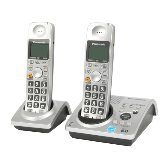
Related Manuals for Panasonic KX-TG1032S


Summary of Contents for Panasonic KX-TG1032S
- Page 1 ORDER NO. KM40612267CE Telephone Equipment KX-TG1032S KX-TG1033S KX-TG1034S KX-TGA101S Expandable Digital Cordless Answering System Silver Version (for U. S. A.) © 2007 Panasonic Communications Co., Ltd. All rights reserved. Unauthorized copying and distribu- tion is a violation of law.
- Page 2 KX-TG1032S/KX-TG1033S/KX-TG1034S/KX-TGA101S...
-
Page 3: Table Of Contents
KX-TG1032S/KX-TG1033S/KX-TG1034S/KX-TGA101S TABLE OF CONTENTS PAGE PAGE 13.1. Circuit Board (Base Unit_Main) ---------------------- 75 1 Safety Precaution ------------------------------------------------ 4 1.1. For Service Technicians --------------------------------- 4 13.2. Circuit Board (Base Unit_Operation)---------------- 77 2 Warning -------------------------------------------------------------- 4 13.3. Circuit Board (Handset) -------------------------------- 79 2.1. -
Page 4: Safety Precaution
KX-TG1032S/KX-TG1033S/KX-TG1034S/KX-TGA101S 1 Safety Precaution 1.1. For Service Technicians ICs and LSIs are vulnerable to static electricity. When repairing, the following precautions will help prevent recurring malfunctions. 1. Cover the plastic parts boxes with aluminum foil and ground them. 2. Ground the soldering irons. -
Page 5: Specifications
KX-TG1032S/KX-TG1033S/KX-TG1034S/KX-TGA101S 2.2.1. Suggested PbF Solder There are several types of PbF solder available commercially. While this product is manufactured using Tin, Silver, and Copper (Sn+Ag+Cu), you can also use Tin and Copper (Sn+Cu) or Tin, Zinc, and Bismuth (Sn+Zn+Bi). Please check the manufacturer’s specific instructions for the melting points of their products and any precautions for using their product with other materials. -
Page 6: Technical Descriptions
KX-TG1032S/KX-TG1033S/KX-TG1034S/KX-TGA101S 4 Technical Descriptions 4.1. Block Diagram (Base Unit) -
Page 7: Circuit Operation (Base Unit)
KX-TG1032S/KX-TG1033S/KX-TG1034S/KX-TGA101S 4.2. Circuit Operation (Base Unit) 4.2.1. Outline Base Unit consists of the following ICs as shown in Block Diagram (Base Unit) (P.6). • DECT BBIC (Base Band IC): IC7 - Handling all the audio, signal and data processing needed in a DECT base unit... - Page 8 KX-TG1032S/KX-TG1033S/KX-TG1034S/KX-TGA101S 4.2.2. Power Supply Circuit The power is supplied to the DECT BBIC, RF Module, EEPROM and Charge Contact from AC Adaptor (+6.5 V) as shown in Fig.101. The power supply is as follows; • DECT BBIC (IC7): CN2 (+6.5 V) → IC1 → Q9 → IC7 CN2 (+6.5 V) →...
- Page 9 KX-TG1032S/KX-TG1033S/KX-TG1034S/KX-TGA101S 4.2.3. Telephone Line Interface <Function> • Bell signal detection • Clip signal detection • ON/OFF hook circuit Bell & Clip (: Calling Line Identification Presentation: Caller ID) signal detection: In the standby mode, Q3 is open to cut the DC loop current and decrease the ring load.
-
Page 10: Block Diagram (Handset)
KX-TG1032S/KX-TG1033S/KX-TG1034S/KX-TGA101S 4.3. Block Diagram (Handset) SPEAKER RXDA Speech Burst Decoding Decoding TXDA RECEIVER Speech Burst Module Encoding Encoding RSSI ADPCM SYDA Codec SYEN Analog Interface Filter SYCL Front Headset CHARGE(+) CHARGE XTAL CHARGE CHARGE CIRCUIT CONTACTS CHARGE DETECT Q4,Q5,Q9 10.368... -
Page 11: Circuit Operation (Handset)
KX-TG1032S/KX-TG1033S/KX-TG1034S/KX-TGA101S 4.4. Circuit Operation (Handset) 4.4.1. Outline Handset consists of the following ICs as shown in Block Diagram (Handset) (P.10). • DECT BBIC (Base Band IC): IC1 - All data signals (forming/analyzing ACK or CMD signal) - All interfaces (ex: Key, Detector Circuit, Charge, DC/DC Converter, EEPROM, LCD) •... -
Page 12: Circuit Operation (Charger Unit)
KX-TG1032S/KX-TG1033S/KX-TG1034S/KX-TGA101S 4.5. Circuit Operation (Charger Unit) 4.5.1. Power Supply Circuit The power supply is as shown. -
Page 13: Signal Route
KX-TG1032S/KX-TG1033S/KX-TG1034S/KX-TGA101S 4.6. Signal Route... - Page 14 KX-TG1032S/KX-TG1033S/KX-TG1034S/KX-TGA101S...
-
Page 15: Location Of Controls And Components
KX-TG1032S/KX-TG1033S/KX-TG1034S/KX-TGA101S 5 Location of Controls and 5.2. Display Components 5.1. Controls 5.1.1. Base Unit 6 Installation Instructions 6.1. Setting up the Base Unit 6.1.1. Connecting the AC adaptor and 5.1.2. Handset telephone line cord... -
Page 16: Setting Up The Handset
KX-TG1032S/KX-TG1033S/KX-TG1034S/KX-TGA101S 6.3. Battery 6.1.2. If you subscribe to a DSL service 6.3.1. Battery installation/replacement 6.2. Setting up the Handset 6.2.1. Connecting the AC adaptor... - Page 17 Battery charge 6.3.3. Battery level 6.3.4. Panasonic battery performance Note for service: The battery strength may not be indicated correctly if the battery is disconnected and connected again, even after it is fully charged. In that case, by recharging the battery as mentioned above, you will get a correct indication of the battery strength.
-
Page 18: Operation Instructions
KX-TG1032S/KX-TG1033S/KX-TG1034S/KX-TGA101S 7 Operation Instructions 7.1. Programmable Settings... - Page 19 KX-TG1032S/KX-TG1033S/KX-TG1034S/KX-TGA101S...
-
Page 20: Registering A Handset
KX-TG1032S/KX-TG1033S/KX-TG1034S/KX-TGA101S 7.2. Registering a Handset 7.2.1. Deregistering a handset 7.3. Copying Handset Phonebook Items You can copy one or all of the phonebook items from one handset to another. -
Page 21: Error Messages
KX-TG1032S/KX-TG1033S/KX-TG1034S/KX-TGA101S 7.4. Error Messages... -
Page 22: Troubleshooting
KX-TG1032S/KX-TG1033S/KX-TG1034S/KX-TGA101S 7.5. Troubleshooting... - Page 23 KX-TG1032S/KX-TG1033S/KX-TG1034S/KX-TGA101S...
- Page 24 KX-TG1032S/KX-TG1033S/KX-TG1034S/KX-TGA101S...
- Page 25 KX-TG1032S/KX-TG1033S/KX-TG1034S/KX-TGA101S...
-
Page 26: Service Mode
KX-TG1032S/KX-TG1033S/KX-TG1034S/KX-TGA101S 8 Service Mode 8.1. Engineering Mode 8.1.1. Base Unit... - Page 27 KX-TG1032S/KX-TG1033S/KX-TG1034S/KX-TGA101S Frequently Used Items (Base Unit) ex.) Items Address Default Data New Data Remarks Frequency 00 01 Use these items in a READ-ONLY mode to confirm the contents. Careless rewriting may 00 10~00 14 Given value cause serious damage to the computer system.
- Page 28 KX-TG1032S/KX-TG1033S/KX-TG1034S/KX-TGA101S 8.1.2. Handset...
- Page 29 KX-TG1032S/KX-TG1033S/KX-TG1034S/KX-TGA101S Frequently Used Items (Handset) ex.) Items Address Default Data New Data Possible Adjusted Possible Adjusted Remarks Value MAX (hex) Value MIN (hex) Battery Low 00 04 (*2) Frequency 00 01 00 10~00 14 Given value Note: (*1) When you enter the address or New Data, please refer to the table below.
-
Page 30: Copying Phonebook Items When Repairing
KX-TG1032S/KX-TG1033S/KX-TG1034S/KX-TGA101S 8.2. Copying Phonebook Items when Repairing You can copy the handset phonebook to another (compatible Panasonic) handset. This will help to save the original phonebook data which the customer has registered. Refer to the following procedures. - Page 31 KX-TG1032S/KX-TG1033S/KX-TG1034S/KX-TGA101S Note: • If the max number of handsets are already registered to the base unit, a new handset cannot be registered. • To register the handset, refer to Registering a Handset (P.20). • ToTo cancel the handset, refer to Deregistering a handset (P.20).
-
Page 32: How To Clear User Setting
KX-TG1032S/KX-TG1033S/KX-TG1034S/KX-TGA101S 8.3. How to Clear User Setting Units are reset to the Factory settings by this operation (Erase recorded Voice messages, stored Phone numbers, Caller list and etc.) Note: • The reset menus differ depending on the following operations. • This operation should not be performed for a usual repair. -
Page 33: Troubleshooting Guide
KX-TG1032S/KX-TG1033S/KX-TG1034S/KX-TGA101S 9 Troubleshooting Guide 9.1. Troubleshooting Flowchart Cross Reference: Check Power (P.34) Bell Reception (P.43) Check Battery Charge (P.35) Check Link (P.36) Check Handset Transmission (P.43) Check Handset Reception (P.43) Signal Route (P.13) Check Caller ID (P.43) Check TAM Operation (P.44) - Page 34 KX-TG1032S/KX-TG1033S/KX-TG1034S/KX-TGA101S 9.1.1. Check Power 9.1.1.1. Base Unit Is the AC Adaptor inserted into AC outlet? (*1) Cross Reference: Note: Power Supply Circuit (P.8) (*1) Refer to Specifications (P.5) for part number and supply voltage of AC Adaptor. 9.1.1.2. Handset Cross Reference:...
- Page 35 KX-TG1032S/KX-TG1033S/KX-TG1034S/KX-TGA101S 9.1.2. Check Battery Charge 9.1.2.1. Base Unit Cross Reference: Charge Circuit (P.11) 9.1.2.2. Handset Cross Reference: Check Power (P.34) Charge Circuit (P.11) 9.1.2.3. Charger Unit Cross Reference: Charge Circuit (P.11)
- Page 36 KX-TG1032S/KX-TG1033S/KX-TG1034S/KX-TGA101S 9.1.3. Check Link 9.1.3.1. Base Unit Cross Reference: Check Point (Base Unit) (P.45) Power Supply Circuit (P.8) Check the RF part (P.38)
- Page 37 KX-TG1032S/KX-TG1033S/KX-TG1034S/KX-TGA101S 9.1.3.2. Handset Cross Reference: Check Point (Handset) (P.45) Power Supply Circuit/Reset Circuit (P.11) Check the RF part (P.38)
- Page 38 KX-TG1032S/KX-TG1033S/KX-TG1034S/KX-TGA101S 9.1.4. Check the RF part 9.1.4.1. Finding out the Defective part After All the Checkings or Repairing 1. Re-register the checked Handset to the checked Base Unit, and Regular HS to Regular BU. Note: If you need to register a handset, refer to Registering a Handset (P.20)
- Page 39 KX-TG1032S/KX-TG1033S/KX-TG1034S/KX-TGA101S 9.1.4.2. RF Check Flowchart Each item (1 ~ 6) of RF Check Flowchart corresponds to Check Table for RF part (P.40). Please refer to the each item. Note: (*1) Base unit - refer to (D) of Check Point (Base Unit) (P.45) Handset - refer to (F) of Check Point (Handset) (P.45)
- Page 40 KX-TG1032S/KX-TG1033S/KX-TG1034S/KX-TGA101S 9.1.4.3. Check Table for RF part Item BU (Base Unit) Check HS (HandSet) Check Link Confirmation Normal 1. Register Regular HS to BU (to be 1. Register HS (to be checked) to Regular checked). HS, BU Mode: [Normal mode] 2.
- Page 41 KX-TG1032S/KX-TG1033S/KX-TG1034S/KX-TGA101S 9.1.4.4. TEST RANGE Check Circuit block which range is defective can be found by the following check. Item BU (Base Unit) Check HS (Handset) Check Range Confirmation TX TEST 1. Register Regular HS to BU (to be checked). 1. Register HS (to be checked) to Regular BU.
- Page 42 KX-TG1032S/KX-TG1033S/KX-TG1034S/KX-TGA101S 9.1.4.5. RF-BBIC Interface Signal Wave Form SYEN SYCL SYDA...
- Page 43 KX-TG1032S/KX-TG1033S/KX-TG1034S/KX-TGA101S 9.1.5. Check Handset Transmission 9.1.6. Check Handset Reception Cross Reference: Signal Route (P.13) Cross Reference: How to Check the Handset Speaker or Receiver (P.65). Signal Route (P.13) 9.1.7. Check Caller ID Cross Reference: Signal Route (P.13) 9.1.8. Bell Reception 9.1.8.1.
- Page 44 KX-TG1032S/KX-TG1033S/KX-TG1034S/KX-TGA101S 9.1.9. Check TAM Operation A) How to change the Auto Disconnect activation (time) Some Telephone Company lines (fiber or cable) ON Hook and OFF Hook voltages are lower than conventional lines, which may cause a malfunction of Auto Disconnect detection. To solve this problem, try changing the Auto Disconnect activation through the procedures below.
-
Page 45: Troubleshooting By Symptom (Base Unit And Charger Unit)
KX-TG1032S/KX-TG1033S/KX-TG1034S/KX-TGA101S 9.2. Troubleshooting by Symptom (Base Unit and Charger Unit) 9.2.1. Check Point (Base Unit) Please follow the items below after repairing. Note: After the measuring, suck up the solder of TP. *: PC Setting (P.56) is required beforehand. The connections of simulator equipments are as shown in Adjustment Standard (Base Unit) (P.58). -
Page 46: How To Replace The Flat Package
KX-TG1032S/KX-TG1033S/KX-TG1034S/KX-TGA101S 9.4. How to Replace the Flat Package IC Even if you do not have the special tools (for example, a spot heater) to remove the Flat IC, with some solder (large amount), a soldering iron and a cutter knife, you can easily remove the ICs that have more than 100 pins. - Page 47 KX-TG1032S/KX-TG1033S/KX-TG1034S/KX-TGA101S 9.4.3. How to Install the IC 1. Temporarily fix the FLAT PACKAGE IC, soldering the two marked pins. *Check the accuracy of the IC setting with the corresponding soldering foil. 2. Apply flux to all pins of the FLAT PACKAGE IC.
-
Page 48: How To Replace The Llp
KX-TG1032S/KX-TG1033S/KX-TG1034S/KX-TGA101S 9.5. How to Replace the LLP (Leadless Leadframe Package) IC 9.5.1. Preparation • PbF (: Pb free) Solder • Soldering Iron Tip Temperature of 700°F ± 20°F (370°C ± 10°C) Note: We recommend a 30 to 40 Watt soldering iron. An expert may be able to use a 60 to 80 Watt iron where someone with less experience could overheat and damage the PCB foil. - Page 49 KX-TG1032S/KX-TG1033S/KX-TG1034S/KX-TGA101S 9.5.4. How to Install the IC 1. Place the solder a little on the land where the radiation GND pad on IC bottom is to be attached. 2. Place the solder a little on the land where IC pins are to be attached, then place the IC.
-
Page 50: Disassembly And Assembly Instructions
KX-TG1032S/KX-TG1033S/KX-TG1034S/KX-TGA101S 10 Disassembly and Assembly Instructions 10.1. Disassembly Instructions 10.1.1. Base Unit... - Page 51 KX-TG1032S/KX-TG1033S/KX-TG1034S/KX-TGA101S...
- Page 52 KX-TG1032S/KX-TG1033S/KX-TG1034S/KX-TGA101S 10.1.2. Handset...
- Page 53 KX-TG1032S/KX-TG1033S/KX-TG1034S/KX-TGA101S 10.1.3. Charger Unit...
- Page 54 KX-TG1032S/KX-TG1033S/KX-TG1034S/KX-TGA101S...
-
Page 55: How To Replace The Handset Lcd
KX-TG1032S/KX-TG1033S/KX-TG1034S/KX-TGA101S 10.2. How to Replace the Handset LCD... -
Page 56: Measurements And Adjustments
KX-TG1032S/KX-TG1033S/KX-TG1034S/KX-TGA101S 11 Measurements and Adjustments 11.1. The Setting Method of JIG (Base Unit) 11.1.1. Preparation 11.1.1.1. Equipment Required • Frequency counter: It must be precise enough to measure intervals of 1 Hz (precision; ±4 ppm). Hewlett Packard, 53131A is recommended. - Page 57 KX-TG1032S/KX-TG1033S/KX-TG1034S/KX-TGA101S 11.1.2.2. Batch file Settings Note: • “****” varies depending on the country. 11.1.2.3. Commands See the table below for frequently used commands. Command name Function Example rdeeprom Read the data of EEPROM Type “rdeeprom 00 00 FF”, and the data from address “00 00”...
-
Page 58: Adjustment Standard (Base Unit)
KX-TG1032S/KX-TG1033S/KX-TG1034S/KX-TGA101S 11.2. Adjustment Standard (Base Unit) When connecting the simulator equipment for checking, please refer to below. 11.2.1. Component View R103 R152 C108 C105 C110 C106 C103 C107 C109 C104 C119 C120 IC10 C121 C128 C126 R109 R151 R110 C127... - Page 59 KX-TG1032S/KX-TG1033S/KX-TG1034S/KX-TGA101S 11.2.2. Flow Solder Side View Note: (A) - (D) is referred to Check Point (Base Unit) (P.45) (*1) is referred to No.3 of Check Table for RF part (P.40)
-
Page 60: Adjustment Standard (Charger Unit)
KX-TG1032S/KX-TG1033S/KX-TG1034S/KX-TGA101S 11.3. Adjustment Standard (Charger Unit) When connecting the simulator equipment for checking, please refer to below. 11.3.1. Flow Solder Side View DC POWER 6.5 V GND (TP4) /2 W Digital Volt Meter... -
Page 61: The Setting Method Of Jig (Handset)
KX-TG1032S/KX-TG1033S/KX-TG1034S/KX-TGA101S 11.4. The Setting Method of JIG (Handset) 11.4.1. Preparation 11.4.1.1. Equipment Required • Frequency counter: It must be precise enough to measure intervals of 1 Hz (precision; ±4 ppm). Hewlett Packard, 53131A is recommended. • DC power: it must be able to output at least 1 A current under 2.4 V for Handset. - Page 62 KX-TG1032S/KX-TG1033S/KX-TG1034S/KX-TGA101S 11.4.2.2. Batch file Settings Note: • “*****” varies depending on the country. 11.4.2.3. Commands See the table below for frequently used commands. Command name Function Example rdeeprom Read the data of EEPROM Type “rdeeprom 00 00 FF”, and the data from address “00 00”...
-
Page 63: Adjustment Standard (Handset)
KX-TG1032S/KX-TG1033S/KX-TG1034S/KX-TGA101S 11.5. Adjustment Standard (Handset) When connecting the simulator equipment for checking, please refer to below. 11.5.1. Component View Note: (A) - (F) is referred to Check Point (Handset) (P.45) (*1) is referred to No.3 of Check Table for RF part (P.40) -
Page 64: Things To Do After Replacing Ic Or X'tal
KX-TG1032S/KX-TG1033S/KX-TG1034S/KX-TGA101S 11.6. Things to Do after Replacing IC or X'tal Cautions: Some of the content on this page may not apply to models from some countries. The contents below are the minimum adjust- ments required for operation. 11.6.1. Base Unit Before making the following adjustment, ensure you have carried out PC Setting (P.56) in The Setting Method of JIG (Base... -
Page 65: How To Check The Handset Speaker Or Receiver
KX-TG1032S/KX-TG1033S/KX-TG1034S/KX-TGA101S 11.7. How to Check the Handset Speaker or Receiver 1. Prepare the digital voltmeter, and set the selector knob to ohm meter. 2. Put the probes at the speaker terminals as shown below. 11.8. Frequency Table (MHz) BASE UNIT... -
Page 66: Schematic Diagram
KX-TG1032S/KX-TG1033S/KX-TG1034S/KX-TGA101S 12 Schematic Diagram 12.1. For Schematic Diagram 12.1.1. Base Unit (Schematic Diagram (Base Unit_Main)) Notes: 1. DC voltage measurements are taken with voltmeter from the negative voltage line. 2. The schematic diagrams may be modified at any time with the development of new technology. - Page 67 KX-TG1032S/KX-TG1033S/KX-TG1034S/KX-TGA101S Memo...
-
Page 68: Schematic Diagram (Base Unit_Main)
KX-TG1032S/KX-TG1033S/KX-TG1034S/KX-TGA101S 12.2. Schematic Diagram (Base Unit_Main) L2T L1T L1R LINE-DC Loop Current For BR For M 100k For BR 2.2k 2.7k 100k 180k K1000p TP-RLY1 L1T/TP-RLY2 1500p L2T/TP-RLY3 For JT 100k L1R/TP-RLY4 180k K1000p TP-RLY5 US-2 US-1 1500p +2.5V Caller ID, For NL +2.5V... - Page 69 KX-TG1032S/KX-TG1033S/KX-TG1034S/KX-TGA101S ANT-2 ANT-1 GND-1 GND-2 GND-3 C122 R152 3.3V +3.3V GND1 GND14 R151 ANT2 GND13 1.5k VCCPA GND12 +2.5V GND2 GND11 TX DATA 10.368MHz IC10 GND3 GND10 RF UNIT VCC_OC ANT1 2.5V R112 RESET GND4 *RESET RSSI RSSI GND9 SYRI...
-
Page 70: Schematic Diagram (Base Unit_Operation)
KX-TG1032S/KX-TG1033S/KX-TG1034S/KX-TGA101S 12.3. Schematic Diagram (Base Unit_Operation) LED2T LED1T CN10-10(KEY1) CN10-9(LED2) CN10-8(VDD) CN10-7(LED1) CN10-6(ROW0) CN10-5(KEY0) CN10-4(ROW2) SKIP REPEAT ERASE CN10-3(ROW1) CN10-2 VOL_UP ANS_ON LOCATOR CN10-1 PLAY STOP VOL_DOWN KX-TG1032/1033/1034 SCHEMATIC DIAGRAM (Base Unit_Operation) - Page 71 KX-TG1032S/KX-TG1033S/KX-TG1034S/KX-TGA101S Memo...
-
Page 72: Schematic Diagram (Handset)
KX-TG1032S/KX-TG1033S/KX-TG1034S/KX-TGA101S 12.4. Schematic Diagram (Handset) 3.3V Charge Current BATTERY +3.3V 3.3V BATT+ 5.6n 2.5V 1.8V +2.5V 2.5V +1.8V 1.8V BATT- 5.6k 115kHz (Talk Mode) 5.6k C149 CHG(+) CHARGE 2.2k Terminal (When on charge) 3.3k K0.01u C107 CHG(-) 1000p C109 0.022 POWER +2.5V... - Page 73 KX-TG1032S/KX-TG1033S/KX-TG1034S/KX-TGA101S ANT_G BATTERY 10.368MHz GND1 GND14 R143 +2.5V ANT2 GND13 2.5V 1.5k VCCPA GND12 RESET GND2 GND11 GND3 GND10 RF Module VCC_OC ANT1 TX DATA GND4 *RESET RSSI RSSI GND9 SYRI TXDA CLK_G GND5 GND8 R51 NC RFCLK RX DATA...
-
Page 74: Schematic Diagram (Charger Unit)
KX-TG1032S/KX-TG1033S/KX-TG1034S/KX-TGA101S 12.5. Schematic Diagram (Charger Unit) SCHEMATIC DIAGRAM (Charger Unit) -
Page 75: Printed Circuit Board
KX-TG1032S/KX-TG1033S/KX-TG1034S/KX-TGA101S 13 Printed Circuit Board 13.1. Circuit Board (Base Unit_Main) 13.1.1. Component View GND-1 L1R/TP-RLY4 GND-3 L2T/TP-RLY3 L1T/TP-RLY2 GND-2 C117 C124 ANT-2 ANT-1 C122 C125 C118 R106 TP23 C153 R102 C101 C140 C155 C102 R163 C112 C111 C129 R92 R91... - Page 76 KX-TG1032S/KX-TG1033S/KX-TG1034S/KX-TGA101S 13.1.2. Flow Solder Side View VDD3 VDD2 VDD1 3.3 V 2.5 V 1.8 V VDD3 3.3V KX-TG103 SPEAKER VDD1 C136 C137 BLACK VDD2 C144 C139 C138 LINE-DC R153 2.5V R117 C154 R161 CHARGE J104 J102 J103 J101 C150 C148...
-
Page 77: Circuit Board (Base Unit_Operation)
KX-TG1032S/KX-TG1033S/KX-TG1034S/KX-TGA101S 13.2. Circuit Board (Base Unit_Operation) 13.2.1. Flow Solder Side View KX-TG103 REPEAT SKIP ANS_ON PQUP11503Z ERASE STOP PLAY LOCATOR VOL_DOWN VOL_UP CN10 KX-TG1032/1033/1034 CIRCUIT BOARD (Base Unit_Operation (Flow Solder Side View)) - Page 78 KX-TG1032S/KX-TG1033S/KX-TG1034S/KX-TGA101S Memo...
-
Page 79: Circuit Board (Handset)
KX-TG1032S/KX-TG1033S/KX-TG1034S/KX-TGA101S 13.3. Circuit Board (Handset) 13.3.1. Component View PQUP11501Z TG103xSR (TGA101) C137 C138 C152 RECEIVER R143 ANT_G RSSI (C58) CLK_G (10.368 MHz) C101 C128 C127 POWER R201 JTAG for JIG R125 2.5 V 3.3 V 1.8V 2.5V 3.3V R202 1.8 V... - Page 80 KX-TG1032S/KX-TG1033S/KX-TG1034S/KX-TGA101S 13.3.2. Flow Solder Side View PQUP11501Z LED10 R141 R140 R142 LED3 LED2 LED1 SOFT_A SOFT_B SOFT_C TALK LEFT RIGHT CANCEL DOWN KX-TGA101 CIRCUIT BOARD (Handset (Flow Solder Side View))
-
Page 81: Circuit Board (Charger Unit)
KX-TG1032S/KX-TG1033S/KX-TG1034S/KX-TGA101S 13.4. Circuit Board (Charger Unit) 13.4.1. Component View PQLV30053Z PQUP11516Z CIRCUIT BOARD (Charger Unit (Component View)) 13.4.2. Flow Solder Side View CIRCUIT BOARD (Charger Unit (Flow Solder Side View)) -
Page 82: Appendix Information Of Schematic Diagram
KX-TG1032S/KX-TG1033S/KX-TG1034S/KX-TGA101S 14 Appendix Information of Schematic Diagram 14.1. CPU Data (Base Unit) 14.1.1. IC7 (BBIC) Pin No. Description Connection at Normal mode at Reset mode *INT1n/ P11 I-PU VDDIO1 VDDIO VDD1 VSS1 SDA1/P25 D,I/O SCL1/P24 *INT5/VDDE/P15 P1[5] *INT2/P12 SP_AMP I-PU... - Page 83 KX-TG1032S/KX-TG1033S/KX-TG1034S/KX-TGA101S Pin No. Description Connection at Normal mode at Reset mode CIDINp CIDINp P14 / *INT4 HOOK P13 / *INT3 TAMIC_CSn ADC2 ADC2 ADC0 ADC0...
-
Page 84: Cpu Data (Handset)
KX-TG1032S/KX-TG1033S/KX-TG1034S/KX-TGA101S 14.2. CPU Data (Handset) 14.2.1. IC1 (BBIC) Pin No. Description Connection at Normal mode at Reset mode INT1n/P1[1] ROW1 I-PU VDDIO VDDIO LED1/PWM0/P2[0] I-PU LED2/PWM1/P2[1] LCD_CSB I-PU LED3 LCD_BACKLIGHT LED_BIAS/P3[6]/PD6 LED_BIAS I-PD SDA1/P2[5] D,IO LCD_SI SCL1/P2[4] LCD_SCL INT5n/VDDE/P1[5] LCD_RS... - Page 85 KX-TG1032S/KX-TG1033S/KX-TG1034S/KX-TGA101S Pin No. Description Connection at Normal mode at Reset mode LDO1_Sence LDO1_Sence AVS2 AVS2 AVD2 AVD2 LSRn/REF LSRn LSRp/REF LSRp MICn VREFm VREFm VBUF VBUF AGND AGND MICp MICp VREFp VREFp P3[0] COL0 I-PD P1[4]/INT4n P1[3]/INT3n ROW3 P2[2]/CLK100 LCD_RESET...
-
Page 86: Terminal Guide Of The Ics, Transistors And Diodes
KX-TG1032S/KX-TG1033S/KX-TG1034S/KX-TGA101S 14.3. Terminal Guide of the ICs, Transistors and Diodes 14.3.1. Base Unit 14.3.2. Handset... -
Page 87: Exploded View And Replacement Parts List
KX-TG1032S/KX-TG1033S/KX-TG1034S/KX-TGA101S 15 Exploded View and Replacement Parts List 15.1. Cabinet and Electric Parts (Base Unit) -
Page 88: Cabinet And Electric Parts (Handset)
(*1) This cable is fixed by welding. Refer to How to Replace the Handset LCD (P.55). (*2) The rechargeable Ni-MH battery HHR-4DPA (Capacity: up to 550 mAh) is available through sales route of Panasonic. (*3) Attach the spacer (No. 122) to the exact location described above. -
Page 89: Cabinet And Electric Parts (Charger Unit)
KX-TG1032S/KX-TG1033S/KX-TG1034S/KX-TGA101S 15.3. Cabinet and Electric Parts (Charger Unit) -
Page 90: Accessories And Packing Materials
KX-TG1032S/KX-TG1033S/KX-TG1034S/KX-TGA101S 15.4. Accessories and Packing Materials 15.4.1. KX-TG1032S... - Page 91 KX-TG1032S/KX-TG1033S/KX-TG1034S/KX-TGA101S 15.4.2. KX-TG1033S...
- Page 92 KX-TG1032S/KX-TG1033S/KX-TG1034S/KX-TGA101S 15.4.3. KX-TG1034S...
- Page 93 KX-TG1032S/KX-TG1033S/KX-TG1034S/KX-TGA101S 15.4.4. KX-TGA101S...
-
Page 94: Replacement Part List
KX-TG1032S/KX-TG1033S/KX-TG1034S/KX-TGA101S 15.5. Replacement Part List Ref. Part No. Part Name & Description Remarks 1. RTL (Retention Time Limited) PQKE10474Y1 CASE, CHARGE TERMINAL PS-HB Note: PQBC10497Z1 BUTTON, MESSAGE AS-HB The marking (RTL) indicates that the Retention Time PQSX10343Z KEYBOARD SWITCH, RUBBER... - Page 95 KX-TG1032S/KX-TG1033S/KX-TG1034S/KX-TGA101S Ref. Part No. Part Name & Description Remarks Ref. Part No. Part Name & Description Remarks ERJ3GEYJ104 100K ECUE1A104KBQ ERJ3GEYJ474 470K ECUV1H221JCV 220P ERJ2GEJ560X ECUV1H221JCV 220P ERJ3GEYJ820 ECUE1C223KBQ 0.022 ERJ3GEYJ821 ECUE1A104KBQ ERJ3GEYJ104 100K ECUV1C104KBV ERJ2GEJ102 ECUE1A104KBQ ERJ3GEYJ104 100K ECUE1A104KBQ...
- Page 96 KX-TG1032S/KX-TG1033S/KX-TG1034S/KX-TGA101S 15.5.1.3. Operational P.C.Board Parts Ref. Part No. Part Name & Description Remarks LED10 B3ACB0000134 (IC FILTERS) Ref. Part No. Part Name & Description Remarks J0JCC0000287 IC FILTER J0JCC0000275 IC FILTER PCB2 PQWP2TG1032H OPERATIONAL P.C.BOARD ASS'Y (RTL) J0JCC0000276 IC FILTER...
- Page 97 ECUE1H100DCQ ECUE1H390JCQ Note: ECUE1H102KBQ 0.001 (*1) You can download and refer to the operating instruc- ECUE1H100DCQ tions (Instruction book) on TSN server. ECUE1H100DCQ ECUE1H100DCQ 15.5.4.1. KX-TG1032S ECUE1H100DCQ ECUE1H471KBQ 470P ECUE1H100DCQ Ref. Part No. Part Name & Description Remarks ECUV1A106ZF ECUE1H100DCQ...
- Page 98 KX-TG1032S/KX-TG1033S/KX-TG1034S/KX-TGA101S Ref. Part No. Part Name & Description Remarks P105 PQPK15670Z GIFT BOX P106 PQXDDS400-8 MAGNET ELECTRIC TRANSDUCER, SECURITY TAG 15.5.4.3. KX-TG1034S Ref. Part No. Part Name & Description Remarks A201 PQLV207V AC ADAPTOR (for Base Unit) A202 PQLV209V AC ADAPTOR (for Charger Unit)