
Related Manuals for Casio CTK-573


Summary of Contents for Casio CTK-573
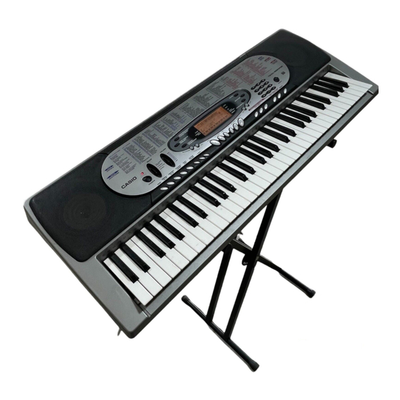
- Page 1 CTK-573 JUL. 2001 LAYER SPLIT ETUDE FULL RANGE CONCERT CHORD PIECE TOUCH RESPONCE FINGERED CASIO CHORD MEMORY NORMAL CTK-573 ELECTRONIC KEYBOARD INDEX...
-
Page 2: Table Of Contents
24 notes maximum (12 for certain tones) Auto Accompaniment Rhythm Patterns: Tempo: Variable (216 steps, = 40 to 255) Chords: 3 fingering methods (CASIO CHORD, FINGERED, FULL RANGE CHORD) Rhythm Controller: START/STOP, INTRO, NORMAL/NORMAL FILL-IN, VARIATION/VARIATION FILL-IN, SYNCHRO/ENDING Accomp Volume: 0 to 127 (128 steps) - Page 3 Other Functions Transpose: 25 steps (–12 semitones to +12 semitones) 101 steps (A4 = approximatery 440Hz ±50Cents) Tuning: Terminals MIDI Terminals: IN, OUT Assignable Jack: Standard jack (sustain, sostenuto, soft, rhythm start/stop) Headphone/ Output Terminal: Stereo standard jack Output Impedance: Output Voltage: 3.0V (RMS) MAX Power Jack:...
-
Page 4: Block Diagram
Assingnable Jack SEG1 ~ SEG40 LCD Driver RAM (256K-bit) MIDI LSI1 DB4 ~ DB7, E, LSI401 RS, R/W TC55257DFL-70L(EL) ML9040-B02GA COM1 ~ COM16 Reset IC RESET S-80940AN MA14 MD0 ~ MD15 Keyboard FI0 ~ FI7 SI0 ~ SI7 Sound Source ROM Sound Source ROM (16M-bit) (8M-bit) -
Page 5: Circuit Description
MEMORY STEP 2 TONE ENDING ONE TOUCH STEP 3 — ACC. VOL. BEAT METRONOME PRESET TRANSPOSE STEP 1 DEMO ETUDE /TONE/MIDI FULL RANGE CASIO NORMAL VARIATION FINGERED NORMAL INTRO START/STOP CHORD CHORD /FILL-IN /FILL-IN PLAY/PAUSE STOP TOUCH LAYER RIGHT RHYTHM... - Page 6 POWER SUPPLY CIRCUIT The power supply circuit generates seven voltages as shown in the following table. VDD voltage is always generated. The others are controlled by APO signal from the CPU. Name Voltage For operation of +5 V CPU, Reset IC, Sound source ROM, RAM, Chip selector DVDD +5.3 V CPU, Sustain jack, MIDI jack, LCD driver...
- Page 7 CPU (LSI4: GT913F) The 16-bit CPU contains a 1k-byte RAM, three 8-bit I/O ports, two timers, a key controller and serial interfaces. The CPU detects key velocity by counting the time between first-key input signal FI and second-key SI from the keyboard.
- Page 8 Pin No. Terminal In/Out Function 57 ~ 76 MA0 ~ MA19 Address bus Chip enable signal output for the sound source ROM and 77, 78 MCSB0, MCSB1 working RAM MCSB2 Not used +5 V source Ground (0 V) source MRDB Read enable signal output for the sound source ROM 83 ~ 98 MD0 ~ MD15...
- Page 9 DAC (IC1: UPD6379GR) The DAC receives 16-bit serial data output from the CPU. The data contains digital sound data of the melody, chord, bass, and percussion for the right and left channels. The DAC converts the data into analog waveforms and output them to each channel separately. Data L OUT Word clock...
- Page 10 FILTER BLOCK Since the sound signals from the DAC are stepped waveforms, the filter block is added to smooth the waveforms. From DAC To main volume POWER AMPLIFIER (IC101: LA4635) The power amplifier is a two-channel amplifier with standby switch. The following table shows the pin function of IC101.
-
Page 11: Adjustment
ADJUSTMENT DISPLAY PCB 1) Items to be adjusted: Item Measuring Instrument Vop voltage setting Voltmeter 2) Adjustment and Test Point Locations (TOP VIEW) TP2 (LSI401 Pin30) TP1 (LSI401 Pin33) 3) Equipment connection/Procedure Vop voltage setting Voltmeter Output Input Input Input Output Output Adjust... -
Page 12: Major Waveforms
MAJOR WAVEFORMS 1 Clock signal for CPU 3 MNI signal LSI4 pin 15 JE connector pin 1 2 Clock signal for CPU 4 APO signal LSI4 pin 16 JC connector pin 12 5 Key common signal KC0 7 CE signal for ROM JB connector pin 1 LSI3 LH536PYE pin 12 6 Key common signal KC1... -
Page 13: Printed Circuit Boards
PRINTED CIRCUIT BOARDS Main PCB JCM702-MA1M Top View LCD PCB JCM702-LCD1M Top View — 12 —... - Page 14 Sub PCB JCM702-MA2M Top View — 13 —...
- Page 15 JCM702-CN1MA Top View Bottom View JCM702-CN2MA Top View Bottom View — 14 —...
-
Page 16: Schematic Diagrams
SCHEMATIC DIAGRAMS Main PCB JCM702-MA1M — 15 —... - Page 17 Sub PCB JCM702-MA2M — 16 —...
- Page 18 Console PCB JCM702-CN1M/CN2M — 17 —...
- Page 19 Display PCB JCM702-LCD1M — 18 —...
- Page 20 Keyboard PCBs JCM618T-KY1M/KY2M — 19 —...
-
Page 21: Exploded View
EXPLODED VIEW — 20 —... -
Page 22: Parts List
PARTS LIST CTK-573 Notes: This parts list does not include the cosmetic parts, which parts are marked with item No. "R-X" in the exploded view. Contact our spare parts department if you need these parts for refurbish. Prices and specifications are subject to change with- out prior notice. - Page 23 PARTS PRICE LIST CTK-573 ITEM CODE NO. PART NAME SPECIFICATION PRICE CODE MAIN PCB 1005 3885 PCB ASSY(MA1M) TK-M241539*1(M702) LSI1 2012 5572 TC55257DFL-70L(EL) LSI2 1004 5604 MSM538002E1FGSKDR1 LSI3 1004 5603 MSM531602F35GSKDR1 LSI4 2012 4998 GT913F 2105 4746 UPD6379GR-E1 1002 9549...
- Page 24 ITEM CODE NO. PART NAME SPECIFICATION PRICE CODE PANEL UNIT 1004 2196 CG1899-TTP 3831 1096 SPEAKER S12J89A 1002 7856 RUBBER/BUTTON M241394-1 6926 3950 RUBBER/BUTTON M340681-1 1005 8895 RUBBER/BUTTON M241389-4 1002 7850 RUBBER/BUTTON M141111-1 1004 1977 RUBBER/BUTTON M241391-2 1005 1796 RUBBER/BUTTON M241392-2 1005 1797 RUBBER/BUTTON...
- Page 25 CASIO TECHNO CO.,LTD. Overseas Service Division Nishi-Shinjuku Kimuraya Bldg. 1F 5-25, Nishi-Shinjuku 7-Chome Shinjuku-ku, Tokyo 160-0023, Japan...