Furuno FAX-30 Service Manual
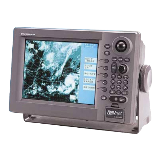
Facsimile receiver
Hide thumbs
Also See for FAX-30:
- Operator's manual (125 pages) ,
- Features (1 page) ,
- Specifications (10 pages)
Table of Contents
Advertisement
Advertisement
Table of Contents

Related Manuals for Furuno FAX-30


Summary of Contents for Furuno FAX-30
- Page 1 Back FACSIMILE RECEIVER FAX-30...
- Page 2 Nishinomiya, 662-8580, JAPAN Telephone : +81-(0)798-65-2111 : +81-(0)798-65-4200 Printed in Japan All rights reserved. Pub. No. SME-62600-B3 (KAOK ) FAX-30 The paper used in this manual is elemental chlorine free. ・FURUNO Authorized Distributor/Dealer A : NOV B3 : DEC . 15, 2010...
-
Page 7: Table Of Contents
Contents Chapter 1 General ...1 Chapter 2 Circuit Description ...2 Chapter 3 Location of Parts ...9 Chapter 4 Maintenance 4.1 Self test ...11 4.2 LED ...12 4.3 Test Point ...12 4.4 Adjustment ...14 4.5 Jumper setting ...14 4.6 DIP Switch setting ...14 4.7 Changing Program ...15... - Page 8 This page is intentionally left blank.
-
Page 9: Chapter 1 General
4) Automatic station selection mode for NAVTEX reception requires position data from the GPS. 5) When both the PC and NavNet are connected, FAX-30 is operated from the PC. 6) Receiving priority (1) In FAX&NAVTEX mode, NAVTEX message is received except for the time set by the timer. -
Page 10: Chapter 2 Circuit Description
Chapter 2 Circuit Description FAX-30 consists of MAIN, RCV and I/F boards. 2.6 m whip antenna + FAX-5, wire antenna or 6 m whip Power supply 12 VDC to 24 VDC NAVNET or PC M connector POWER LED MJ3P connector... - Page 11 MAIN board (08P3218) MAIN board consists of CPU, NET and PWR circuits. CPU circuit CPU consists of 32-bit CPU&DSP with a built-in Ethernet controller, 24-bit CODEC (AD converter), Flash ROM and SDRAM. The main function of CPU&DSP (U18) is as follows. 1) Filtering of received signal (DSP) 2) Demodulation of FAX data (DSP) 3) Demodulation of NAVTEX data (DSP)
- Page 12 NET circuit Net circuit is Ethernet 10Base-T interface circuit using TCP/IP protocol. U2 is a full feature Physical Layer device with integrated PMD (Physical Medium Dependant) sublayers to support 10Base-T Ethernet protocol. PWR circuit Fig.4 shows the block diagram of power supply circuit. The power supply circuit employs a floating type flyback switching regulator.
- Page 13 Power Supply Specification Input voltage: 10.8 Vdc to 31.2 Vdc Power consumption: 12 W (Maximum) Input current: 1.0 A or less (12 V) and 0.5 A or less (24 V) Protection circuit PWR circuit is protected by; Output short-circuit protector; 3.3 V line: U17 includes a protector. Input low- and over-voltage protector;...
- Page 14 RCV board (08P3219) Three bandpass filters, FL1, FL2 and FL3 locate at the first stage of the receiver. The filter passes the following frequencies. When receiving NAVTEX message, FL3 is used. FL1: 2 MHz to 13.2 MHz FL2: 13.2 MHz to 25 MHz FL3: 80 kHz to 518 kHz The shift register, U10 receives three signals, RCV DATA, RCV CLK and RCV BAND from MAIN board to select the filter.
- Page 15 The synthesizer consists of 18 MHz oscillator, Direct Digital Synthesizer (DDS), PLL and VCO. The signals from MAIN board, RCV DATA, RCV CLK, RCV DDS, RCV PLL and RCV BAND, determines the frequency of the local oscillator depending on the selected receiving frequency. When the synthesizer unlocks, RCV UNLOCK signal is generated for the error message.
- Page 16 CPU generates RCV TEST signal at the self test. Receiving this signal, the switch, Q11 turns on and 18 MHz test signal is supplied to the antenna terminal. Item Receiving frequency Emission mode Antenna impedance First IF signal Second IF signal Synthesizer Power supply to pre-amplifier I/F board (08P3220)
-
Page 17: Chapter 3 Location Of Parts
Chapter 3 Location of Parts RCV board (08P3219) MAIN board (08P3218) IF board (08P3220) ANT connector POWER connector LAN connector (Network) Fig.6 FAX-30, with cover removed... - Page 18 (ACT/WIRE) Filter 1, 2 and 3 TP11 (0V) TP1 (SWF) TP5 (AGC) TP3 (0V) TP4 (VC0) Fig.7 RCV board (08P3219) R51 TP7 (5V) J13 TP8 (15V) CR9 (G) Fig.8 MAIN board (08P3218) Chapter 3 Location of Parts TP1 (0V) TP12 (0V) TP6 (+5V) TP8 (2nd L0) TP10 (18 MHz)
-
Page 19: Chapter 4 Maintenance
The self-test is performed by using the procedure below. 1. Press [MENU] on NavNet display. 2. Press “FAX-30 SYSTEMSETUP”. 3. Press “TEST” to start the test. The result appears as shown in Fig.9. 4. Press “RETURN” to return to the SYSTEM SETUP display. -
Page 20: Led
4.2 LED POWER LED (CR9, green) on MAIN board blinks as follows. 1) When loading the image at power-up; ON: 0.2 seconds, OFF: 0.2 seconds 2) At normal operation; ON: 1 second, OFF: 1 second 4.3 Test Point The following signals appear at the test points. MAIN board (08P3218) TP No. - Page 21 RCV board (08P3219) Signal TP No. name V=0.8 Vpp to 1.5 Vpp 2.99999 MHz: 8.0 V to 9.5V 29.654950 MHz to 29.655130 MHz SG level 50 dBµ: 1.0 V or more SG level 110dBµ: 7.0 V or more +5 V 4.75 V to 5.25 V 1st LO 2MHz...
-
Page 22: Adjustment
4.4 Adjustment Following adjusters locate on MAIN and RCV boards. Board Adjuster MAIN board RCV board 4.5 Jumper setting J23 on RCV board is used as below. When +12 V is supplied to the antenna: Set J23 to ACT (#1 and #2) When no power is supplied to the antenna: Set J23 to WIRE (#3 and #2, factory-default) 4.6 DIP Switch setting S1 on MAIN board is used as below. -
Page 23: Changing Program
5) Setup.bat Procedure 1. Disconnect the power cable of FAX-30. 2. Connect a PC to “NETWORK (LAN)” connector of FAX-30, using the cross cable 9 pin D-sub 6 pin MJ cable. 3. Change the IP address of PC to “172.31.1.1”. - Page 24 This page is intentionally left blank.
-
Page 25: Facsimile Receiver
( 0 0 0 - 5 7 0 - 2 9 9 ) A 高 高 高 高 橋 橋 橋 橋 TITLE ファクシミリ受画装置 高 高 高 高 FAX-30 橋 橋 橋 橋 FACSIMILE RECEIVER 三 三 三 三 好 好 好 好 C6260-E01-A DWG. NO. - Page 26 型式 PRINTED CIRCUIT BOARD 08P3218, MAIN 08P3219, RCV 08P3220, I/F FUSE FGMB 2A 125V CONNECTOR M-R-A3-3 (NI) CABLE w/CONNECTOR 08-156 (6-6P) 08-158 (3-3P) Model FAX-30 Unit ファクシミリ受画装置 FACSIMILE RECEIVER Ref.Dwg. C6260-K01-A Blk.No. CODE No. REMARKS コード番号 コード番号 コード番号 コード番号 備考...