Table of Contents
Advertisement
Quick Links
TABLE OF CONTENTS
1 Safety Precautions----------------------------------------------- 3
1.1. General Guidelines---------------------------------------- 3
1.2. Before Repair and Adjustment ------------------------- 4
1.3. Protection Circuitry ---------------------------------------- 4
1.4. Safety Part Information----------------------------------- 4
2 Warning -------------------------------------------------------------- 5
to Electrostatically Sensitive (ES) Devices---------- 5
3 Service Navigation ----------------------------------------------- 7
3.1. Service Information --------------------------------------- 7
4 Specifications ----------------------------------------------------- 8
4.1. Others (Licenses)------------------------------------------ 8
5 General/Introduction -------------------------------------------- 9
5.1. About the power of this unit ----------------------------- 9
5.2. About the DC OUT terminal (USB)-------------------- 9
6 Location of Controls and Components ------------------11
Wireless Speaker System
Model No.
Product Color: (K)...Black Type (For NA30P/PC)
PAGE
6.1. Main Unit Key Button Operations -------------------- 11
7 Service Mode ----------------------------------------------------- 12
7.1. Service Mode --------------------------------------------- 12
7.2. Doctor Mode----------------------------------------------- 13
7.3. Version Display Mapping------------------------------- 14
8 Troubleshooting Guide --------------------------------------- 15
9 Disassembly and Assembly Instructions--------------- 16
9.1. Disassembly flow chart --------------------------------- 17
9.2. Types of Screws------------------------------------------ 17
9.3. Main Parts Location Diagram ------------------------- 18
9.4. Disassembly of Rear Cabinet Block----------------- 19
(SP5) -------------------------------------------------------- 20
9.6. Disassembly of Jack P.C.B. --------------------------- 21
9.7. Disassembly of NFC P.C.B. --------------------------- 22
9.8. Disassembly of Bluetooth Module ------------------- 23
9.9. Disassembly of Battery Pack-------------------------- 24
9.10. Disassembly of Main P.C.B. --------------------------- 25
© Panasonic Corporation 2013. All rights reserved.
Unauthorized copying and distribution is a violation of
law.
SC-NA30GN
SC-NA30P
SC-NA30PC
(S)...Silver Type (For NA30GN/P)
PSG1310005CE
A6
PAGE
Advertisement
Table of Contents

Related Manuals for Panasonic SC-NA30GN


Summary of Contents for Panasonic SC-NA30GN
-
Page 1: Table Of Contents
5.3. One-Touch Connection (Connecting by NFC) ----10 9.9. Disassembly of Battery Pack-------------------------- 24 9.10. Disassembly of Main P.C.B. --------------------------- 25 6 Location of Controls and Components ------------------11 © Panasonic Corporation 2013. All rights reserved. Unauthorized copying and distribution is a violation of law. - Page 2 9.11. Disassembly of Woofer Speaker (SP3)------------- 27 9.12. Disassembly of Tweeter Speaker (SP1) & (SP2) -------------------------------------------------------- 28 9.13. Disassembly of Mic Unit -------------------------------- 29 9.14. Disassembly of Top Ornament Block --------------- 29 9.15. Replacement of Top Ornament ----------------------- 30 9.16. Disassembly of Volume P.C.B.------------------------ 31 9.17.
-
Page 3: Safety Precautions
1 Safety Precautions 1.1. General Guidelines 1. IMPORTANT SAFETY NOTICE There are special components used in this equipment which are important for safety. These parts are marked by in the Schematic Diagrams, Circuit Board Layout, Exploded Views and Replacement Parts List. It is essential that these critical parts should be replaced with manufacturer’s specified parts to prevent X-RADIATION, shock, fire, or other hazards. -
Page 4: Before Repair And Adjustment
1.2. Before Repair and Adjustment Caution : DO NOT SHORT-CIRCUIT DIRECTLY (with a screwdriver blade, for instance), as this may destroy solid state devices. After repairs are completed, restore power gradually using a variac, to avoid overcurrent. • Current consumption at AC 240V, at 50Hz during power on at volume minimum, (Selector : AUX mode) should be ~200 mA. (For •... -
Page 5: Warning
2 Warning 2.1. Prevention of Electrostatic Discharge (ESD) to Electrostatically Sensi- tive (ES) Devices Some semiconductor (solid state) devices can be damaged easily by static electricity. Such components commonly are called Elec- trostatically Sensitive (ES) Devices. The following techniques should be used to help reduce the incidence of component damage caused by electrostatic discharge (ESD). -
Page 6: Service Caution Based On Legal Restrictions
2.2. Service caution based on Legal restrictions 2.2.1. General description about Lead Free Solder (PbF) The lead free solder has been used in the mounting process of all electrical components on the printed circuit boards used for this equipment in considering the globally environmental conservation. The normal solder is the alloy of tin (Sn) and lead (Pb). -
Page 7: Service Navigation
3 Service Navigation 3.1. Service Information This service manual contains technical information which will allow service personnel’s to understand and service this model. Please place orders using the parts list and not the drawing reference numbers. If the circuit is changed or modified, this information will be followed by supplement service manual to be filed with original service manual. -
Page 8: Specifications
4 Specifications AC Adaptor Input: (For GN) AC 100 V to 240 V 50/60 Hz 1000 mA Input: (For P/PC) AC 100 V to 240 V 50/60 Hz Amplifier Section 800 mA RMS Output Power (AC Adaptor) Output: DC 12 V 3A Normal Mode 10% total harmonic distortion General... -
Page 9: General/Introduction
5 General/Introduction 5.1. About the power of this unit 5.2. About the DC OUT terminal (USB) -
Page 10: One-Touch Connection (Connecting By Nfc)
5.3. One-Touch Connection (Connecting by NFC) -
Page 11: Location Of Controls And Components
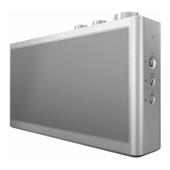
6 Location of Controls and Components 6.1. Main Unit Key Button Operations... -
Page 12: Service Mode
7 Service Mode This unit is equipped with features of service mode & doctor mode setting for checking the functions & reliability. 7.1. Service Mode Here is the procedures to enter into Service Mode. Step 1 : Turn on the unit. Step 2 : Press and hold [BT] →... -
Page 13: Doctor Mode
7.2. Doctor Mode Here is the procedures to enter into Doctor Mode. Step 1 : Turn on the unit. Step 2 : Press and hold [LP] → [LP + POWER] → [LP + POWER + VOL+] on the unit. Step 3 : LP LED start blinking with 250ms (Refer to Figure 7-2). To exit the Doctor Mode •... -
Page 14: Version Display Mapping
7.3. Version Display Mapping Version POWER Remarks Bit 2 Bit 1 Bit 0 No use in this blank pattern 01,08,15,22,,,,,71,78,85,92,99… 02,09,16,23,,,,,72,79,86,93,100… 03,10,17,24,,,,73,80,87,94,101... 04,11,18,25,,,,,74,81,88,95,102… 05,12,19,26,,,,,75,82,89,96,103… 06,13,20,27,,,,,76,83,90,97,104… 07,14,21,28,,,,,77,84,91,98,105… Link Status “O” means LED on “X” means LED off “*” means LED blink 250ms Table 7-1... -
Page 15: Troubleshooting Guide
8 Troubleshooting Guide This section is not available at the time of issue... -
Page 16: Disassembly And Assembly Instructions
9 Disassembly and Assembly Instructions Caution Note: • This section describes the disassembly and/or assembly procedures for all major printed circuit boards & main compo- nents for the unit. (You may refer to the section of “Main components and P.C.B Locations” as described in the service manual) •... -
Page 17: Disassembly Flow Chart
9.1. Disassembly flow chart The following chart is the procedure for disassembling the casing and inside parts for internal inspection when carrying out the ser- vicing. To assemble the unit, reverse the steps shown in the chart below. 9.2. Types of Screws... -
Page 18: Main Parts Location Diagram
9.3. Main Parts Location Diagram... -
Page 19: Disassembly Of Rear Cabinet Block
9.4. Disassembly of Rear Cabinet Step 2 : Remove 4 Screw Ornaments. Caution : Replace the Screw Ornaments if they are torn Block during disassembling. Step 1 : Remove 2 Foot Rubbers. Caution : Replace the Foot Rubbers if they are torn during disassembling. -
Page 20: Disassembly Of Passive Radiator Unit (Sp4) & (Sp5)
Step 4 : Slightly lift up the Rear Cabinet Block. 9.5. Disassembly of Passive Radia- tor Unit (SP4) & (SP5) Picture shows the location of the Passive Radiator Unit (SP4) & (SP5). Step 5 : Remove the Rear Cabinet Block. Note : The disassembling procedure for Passive Radiator Unit (SP4) will be described only. -
Page 21: Disassembly Of Jack P.c.b
Step 2 : Remove the Passive Radiator Unit (SP4). 9.6. Disassembly of Jack P.C.B. • Refer to “Disassembly of Rear Cabinet Block” Step 1 : Lift up the 6P FFC & 17P FFC from the Slot. Caution : During assembling, ensure that the 6P FFC & 17P FFC is properly seated into the slots. -
Page 22: Disassembly Of Nfc P.c.b
Step 3 : Detach 17P FFC at connector (P1902) on the Jack 9.7. Disassembly of NFC P.C.B. P.C.B.. • Refer to “Disassembly of Rear Cabinet Block” Step 4 : Detach 6P FFC at connector (P1901) on the Jack P.C.B.. Step 5 : Remove the Jack P.C.B.. Step 1 : Lift up the 11P FFC from the Slot. -
Page 23: Disassembly Of Bluetooth Module
Step 3 : Detach 11P FFC at connector (P1301) on the NFC 9.8. Disassembly of Bluetooth Mod- P.C.B.. Step 4 : Remove the NFC P.C.B.. • Refer to “Disassembly of Rear Cabinet Block” Step 1 : Remove 1 screw. Step 2 : Detach 16P FFC at connector (CN1701) on the Blue- tooth Module. -
Page 24: Disassembly Of Battery Pack
Caution : During assembling, ensure that the Bluetooth 9.9. Disassembly of Battery Pack Module is properly seated into the locator. • Refer to “Disassembly of Rear Cabinet Block” Step 1 : Remove 2 screws. Step 2 : Slightly lift up the Battery Pack. Step 3 : Remove the Battery Holder (L) and Battery Holder (R). -
Page 25: Disassembly Of Main P.c.b
Step 5 : Remove the Battery Pack. 9.10. Disassembly of Main P.C.B. • Refer to “Disassembly of Rear Cabinet Block” • Refer to “Disassembly of Battery Pack” Step 1 : Detach 2P cable at connector (P1403) on the Main P.C.B.. Step 2 : Detach 11P FFC at connector (P1005) on the Main P.C.B.. - Page 26 Step 9 : Remove 4 screws. Caution : During assembling, ensure that the Main P.C.B. is properly seated into the locator. Step 10 : Slightly lift up the Main P.C.B.. Step 11 : Detach 8P FFC at connector (P1003) on the Main P.C.B..
-
Page 27: Disassembly Of Woofer Speaker (Sp3)
9.11. Disassembly Woofer Caution : During assembling, ensure that the Woofer Speaker Terminal is facing the Top Ornament Block. Speaker (SP3) • Refer to “Disassembly of Rear Cabinet Block” • Refer to “Disassembly of Battery Pack” • Refer to “Disassembly of Main P.C.B.” Step 1 : Remove 4 screws. -
Page 28: Disassembly Of Tweeter Speaker (Sp1) & (Sp2)
9.12. Disassembly Tweeter Step 2 : Remove the Tweeter Speaker (SP1). Speaker (SP1) & (SP2) Picture shows the location of the Tweeter Speaker (SP1) & (SP2). Note : The disassembling procedure for Tweeter Speaker (SP1) will be described only. For Tweeter Speaker (SP2) please refer to the same procedure described here. -
Page 29: Disassembly Of Mic Unit
9.13. Disassembly of Mic Unit 9.14. Disassembly of Top Ornament • Refer to “Disassembly of Rear Cabinet Block” Block • Refer to “Disassembly of Battery Pack” • Refer to “Disassembly of Rear Cabinet Block” • Refer to “Disassembly of Main P.C.B.” Step 1 : Remove 2 screws. -
Page 30: Replacement Of Top Ornament
9.15. Replacement of Top Ornament 9.15.2. Assembly of Top Ornament • Refer to “Disassembly of Top Ornament Block” Step 1 : Slide the Guide Plate to the right until it come to a stop. 9.15.1. Disassembly of Top Ornament Step 2 : Ensure the Guide Arm is in left position as shown. Step 1 : Release 2 catches. -
Page 31: Disassembly Of Volume P.c.b
Caution 1 : Slide the Guide Plate to the Left and then to the 9.16. Disassembly of Volume P.C.B. Right to check that the Top Ornament fixed in properly. • Refer to “Disassembly of Top Ornament Block” Caution 2 : During assembling, ensure that the Top Orna- ment in open condition before fix to the Rear Cabinet •... - Page 32 Step 3 : Release 4 catches. Step 6 : Remove the Volume P.C.B.. Caution : During assembling, ensure the Volume Holder is fully catched and properly seated on the locator. Caution : During assembling, ensure the Volume P.C.B. is properly seated on the locator. Step 4 : Remove the Volume Holder.
-
Page 33: Replacement Of Gear Box Assembly
9.17. Replacement Gear 9.17.2. Assembly of Gear Box Assembly Assembly Step 1 : Slot in the Gear Box Assembly into Volume Holder. • Refer to “Disassembly of Top Ornament Block” Step 2 : Press down the Gear Box Assembly. • Refer to “Disassembly of Top Ornament” 9.17.1. - Page 34 9.17.3. Disassembly of Motor P.C.B. Step 4 : Desolder pins on the solder side of the Motor P.C.B. and remove the Motor P.C.B.. • Refer to “Disassembly of Gear Box Assembly” Step 1 : Release the 2P Wire from the slots. Step 2 : Remove 1 screw.
- Page 35 9.17.4. Disassembly of Belt & Pulley Gear 9.17.5. Disassembly of Motor Assembly • Refer to “Disassembly of Gear Box Assembly” • Refer to “Disassembly of Gear Box Assembly” • Refer to “Disassembly of Motor P.C.B.” Step 1 : Remove the Belt. •...
- Page 36 Caution 1 : During assembling, position & align the Motor 9.17.7. Disassembly of Drive Gear wire with the indicated arrow on the Gear Box Assembly. • Refer to “Disassembly of Gear Box Assembly” Caution 2 : During assembling, ensure the Motor Assembly •...
-
Page 37: Disassembly Of Guide Plate Block
9.18. Disassembly of Guide Plate Caution : During assembling, ensure the Guide Plate is properly fixed as picture shown. Block • Refer to “Disassembly of Top Ornament Block” • Refer to “Disassembly of Top Ornament” • Refer to ““Disassembly of Volume P.C.B.” •... -
Page 38: Service Position
10 Service Position Note: For description of the disassembly procedures, see the Section 9 10.1. Checking of Main P.C.B. (Side B) Step 13 : Connect 6P wire at connector (P1802) on the Main Step 1 : Remove the Rear Cabinet Block. P.C.B.. -
Page 39: Checking Of Main P.c.b. (Side A)
Step 16 : Check the Main P.C.B. (Side B) according to the dia- 10.2. Checking of Main P.C.B. (Side gram shown. • Refer to (Step 1) - (Step 12) of item 10.1. Step 1 : Flip over the Main P.C.B., NFC P.C.B., Bluetooth Mod- ule &... - Page 40 Step 4 : Check the Main P.C.B. (Side A) according to the dia- gram shown.
-
Page 41: Block Diagram
TH TEMP DET P10 34 TH TEMP DET BAT DET P13 37 BAT DET ACOK P51 3 ACOK TO SYSTEM CONTROL & AUDIO BLOCK (2/2) NOTE: “ * ” REF IS FOR INDICATION ONLY SC-NA30GN/P/PC SYSTEM CONTROL & AUDIO (1/2) BLOCK DIAGRAM... -
Page 42: System Control & Audio (2/2) Block Diagram
AUX R-IN 14 AINR P1901 P1811 AUX L-IN AUX L-IN 13 AINL IC1501 C0FBAY000032 STEREO A/D CONVERTER TO SYSTEM CONTROL & AUDIO BLOCK (1/2) NOTE: “ * ” REF IS FOR INDICATION ONLY SC-NA30GN/P/PC SYSTEM CONTROL & AUDIO (2/2) BLOCK DIAGRAM... -
Page 43: Power Supply Block Diagram
8.4V PW +B PW +B QR1855 IC1852 ADPT CNT ADPT CNT SWITCH C0DBAYY01896 VOLTAGE REGULATOR PW +B 8.4V BOOT 1 LP EN LP EN FB 5 NOTE: “ * ” REF IS FOR INDICATION ONLY SC-NA30GN/P/PC POWER SUPPLY BLOCK DIAGRAM... -
Page 44: Wiring Connection Diagram
12 Wiring Connection Diagram MOTOR P.C.B. VOLUME P.C.B. SOLDER SIDE SOLDER SIDE P1931 VR1921 VR1922 VR1923 1 ..5 1 ..8 P1922 TL1932* TL1931* P1923 (RED) (BLACK) 5 . -
Page 45: Schematic Diagram
13 Schematic Diagram 13.1. Schematic Diagram Notes • Voltage and signal line (All schematic diagrams may be modified at any time with : +B Signal Line the development of new technology) Notes: S1921: RESET switch. S1931: POS_SW1 switch. S1932: POS_SW2 switch. •... -
Page 47: Main (Audio In) Circuit
13.2. MAIN (AUDIO IN) CIRCUIT SCHEMATIC DIAGRAM - 1 MAIN (AUDIO IN) CIRCUIT R1513 MIC_BIAS C1517 C1516 C1534 MIC_IN_P C1528 1000P R1512 LB1503 J0JCC0000059 P1501 C1513 220P MIC_IN_P TO MIC UNIT MIC_IN_N R1516 C1535 MIC_IN_N DGND AGND IC1501 AUX_SDO C0FBAY000032 A/D CONVERTER G_AUX_BCK AUX_WCK... -
Page 48: Main (Micon) Circuit
13.3. MAIN (MICON) CIRCUIT SCHEMATIC DIAGRAM - 2 MAIN (MICON) CIRCUIT : +B SIGNAL LINE R1076 R1090 R1091 R1075 OUT2 C1025 10 R1074 C1024 VREF R1077 IC1004 R1073 C0GBY0000079 R1092 MOTOR DRIVER RL1013* RL1012* PW_SW5R0V BAT_ERR R1051 LP_EN DEBUG_TX R1052 VBUS_CHG_DET DEBUG_RX R1087... -
Page 49: Main (Damp) Circuit
13.4. MAIN (DAMP) CIRCUIT SCHEMATIC DIAGRAM - 3 MAIN (DAMP) CIRCUIT LB1401 J0JHC0000046 PW_DSP_SW8R4V LB1402 J0JHC0000046 AMP_GND C1446 DAMP_SLEEP R1427 R1429 DAMP_CKMOD C1447 R1430 DAMP_MUTE R1417 Q1402 100K R1428 B1ABCF000011 R1419 D1406 SWITCH DA2J10100L C1457 D1405 C1456 24 23 C1437 C1436 DA2J10100L 1000P... -
Page 50: Main (Power) Circuit
13.5. MAIN (POWER) CIRCUIT SCHEMATIC DIAGRAM - 4 MAIN (POWER) CIRCUIT Q1853 B1CHRC000047 POWER SUPPLY R1871 C1883 R1876 R1869 470K QR1855 C1854 R1853 ADPT_CNT B1GBCFNN0041 SWITCH IC1852 C0DBAYY01896 VOLTAGE REGULATOR R1891 L1851 G1C4R7Z00014 BOOT PW_DSP_SW8R4V R1872 R1855 330K C1890 PW_+B 180P R1890 5.6K... -
Page 51: Main (Charger) Circuit
13.6. MAIN (CHARGER) CIRCUIT SCHEMATIC DIAGRAM - 5 MAIN (CHARGER) CIRCUIT : +B SIGNAL LINE P1801 Q1802 B1CFRD000076 C1819 D1812 R1807 SWITCH DC-IN B0JCRD000025 2200P DC-IN PW_+B DC-IN C1817 R1805 270K C1818 USB_VBUS Q1804 DGND PW_USB_SW5R0V JACK CIRCUIT USB_VBUS R1806 FC8J33040L LB1801 J0JHC0000046... -
Page 52: Jack, Volume & Motor Circuit
13.7. JACK, VOLUME & MOTOR CIRCUIT SCHEMATIC DIAGRAM - 6 JACK CIRCUIT MOTOR CIRCUIT : +B SIGNAL LINE S1921 RESET P1901 (BLACK) TL1931* RESET P1931 AUX_DET LOADING MAIN (CHARGER) CIRCUIT AUX R-IN MOTOR* (P1811) AUX L-IN VOLUME CIRCUIT IN SCHEMATIC POS_SW1 (P1923) (RED) -
Page 53: Printed Circuit Board
14 Printed Circuit Board 14.1. MAIN P.C.B. (Side A) MAIN P.C.B. (REP5023A) R1555 R1029 R1032 R1030 R1027 R1028 R1082 C1825 R1031 R1081 R1075 R1053 R1052 C1854 Q1402 R1853 IC1004 RL1013* RL1012* R1074 R1417 C1856 R1854 C1855 R1006 R1037 C1001 C1024 R1884 R1003 R1508... -
Page 54: Main P.c.b. (Side B)
14.2. MAIN P.C.B. (Side B) MAIN P.C.B. (REP5023A) P1005 (TO NFC P.C.B.) C1525 R1046 R1051 IC1504 P1811 1 2 3 P1003 D1406 C1552 C1551 R1033 C1457 R1895 Q1851 P1403 R1055 QR1853 R1894 R1005 C1459 C1026 R1078 SUBWOOFER R1878 C1873 R1083 SPEAKERS) R1851 C1885... -
Page 55: Jack, Volume & Motor P.c.b
14.3. JACK, VOLUME & MOTOR P.C.B. JACK P.C.B. (REP5024AA) P1902 P1901 CK1905 CK1901 CK1909 CK1921 C1910 CK1914 CK1907 CK1903 CK1917 L1902 L1903 L1901 CK1911 CK1904 CK1908 CK1902 CK1920 C1902 C1901 IP1901 CK1906 LB1901 C1903 R1903 0.15A S1921 (RESET) 3702AA 3702AA P1903 (FOR FIRMWARE 3702AA... -
Page 57: Appendix Information Of Schematic Diagram
15 Appendix Information of Schematic Diagram 15.1. Voltage Measurement & Waveform Chart Note: • Indicated voltage values are the standard values for the unit measured by the DC electronic circuit tester (high-impedance) with the chassis taken as standard. Therefore, there may exist some errors in the voltage values, depending on the internal impedance of the DC circuit tester. •... - Page 58 15.1.2. MAIN P.C.B. (2/3) IC1402 REF NO. MODE POWER ON 11.8 11.8 STANDBY 11.8 11.8 IC1501 REF NO. MODE POWER ON STANDBY IC1802 REF NO. MODE POWER ON 11.3 11.9 11.8 13.2 10.4 11.1 STANDBY 11.3 11.9 11.8 13.2 10.4 11.1 IC1831 REF NO.
- Page 59 15.1.3. MAIN P.C.B. (3/3) Q1803 Q1804 REF NO. MODE POWER ON 11.9 11.8 11.8 11.9 STANDBY 11.9 11.8 11.8 11.9 Q1851 Q1853 QR1801 REF NO. MODE POWER ON 11.8 11.8 11.8 11.8 11.8 11.8 11.8 STANDBY 11.8 11.8 11.8 11.8 11.8 11.8 11.8 QR1802 QR1830 QR1853...
-
Page 61: Exploded View And Replacement Parts List
(JACK P.C.B.) S1921 P1903 JK1902 JK1903 (BLUETOOTH JK1904 MODULE P.C.B.) S1931 P1931 P1501 P1402 P1003 P1802 S1932 P1811 P1401 P1403 (MOTOR P.C.B.) P1005 P1002 (MAIN P.C.B.) P1801 P1006 VR1922 P1923 VR1923 VR1921 P1922 (VOLUME P.C.B.) SC-NA30P-K/S SC-NA30PC-K SC-NA30GN-S CABINET DRAWINGS... - Page 62 16.1.2. Packaging (for SC-NA30PC-K SC-NA30GN-S) AC CORD ACCESSORIES BAG (FOR GN ONLY) **PAD A3 O/I BOOK AC ADAPTOR A4 CARRYING POUCH (FOR GN ONLY) SC-NA30PC/GN POLYFOAM (LEFT) POLYFOAM (RIGHT) SC-NA30PC-K SC-NA30GN-S NOTE: " ** " PART IS NOT SUPPLIED. PACKAGING DRAWINGS...
- Page 63 16.1.3. Packaging (for SC-NA30P-K/S) *PAD SC-NA30P *PAD ACCESSORIES BAG A3 O/I BOOK *PAD *CUSHION AC ADAPTOR SC-NA30P-K/S NOTE: " * " PART IS NOT SUPPLIED. PACKAGING DRAWINGS...
- Page 65 16.1.4. Mechanical Replacement Parts List Safety Ref. No. Part No. Part Name & Qty Remarks Description Safety Ref. No. Part No. Part Name & Qty Remarks RFKHCNA30EBK REAR CABINET P/PC-K Description ASS’Y RFKHCNA30EBS REAR CABINET P/GN-S CABINET AND ASS’Y CHASSIS RMN1071A BATTERY HOLDER R 1 RMR2139-C...
- Page 66 Safety Ref. No. Part No. Part Name & Qty Remarks Description RMN1071 BATTERY HOLDER L 1 SPEAKERS L0AA05A00104 TWEETER SPEAKER L0AA05A00104 TWEETER SPEAKER L0AA08A00041 WOOFER SPEAKER RAQ0102 PASSIVE RADIA- TOR UNIT RAQ0102 PASSIVE RADIA- TOR UNIT PACKING MATERI- RPK3022 PACKING CASE RPK3023 PACKING CASE PC-K...
-
Page 67: Electrical Replacement Parts List
16.2. Electrical Replacement Parts List Safety Ref. No. Part No. Part Name & Qty Remarks Description Safety Ref. No. Part No. Part Name & Qty Remarks Q1402 B1ABCF000011 TRANSISTOR (E.S.D) Description Q1802 B1CFRD000076 TRANSISTOR (E.S.D) Q1803 FC8J33040L TRANSISTOR (E.S.D) PRINTED CIR- Q1804 FC8J33040L TRANSISTOR... - Page 68 Safety Ref. No. Part No. Part Name & Qty Remarks Safety Ref. No. Part No. Part Name & Qty Remarks Description Description VR1922 D2BDA14Y0003 TREBLE JOG VR1923 D2BDA14Y0003 BASS JOG IP1891 D4FB1R100015 RESETTABLE FUSE SWITCHES PROTECTOR S1921 EVQPC105K SW RESET IP1901 D1JBR015A007 PROTECTOR...
- Page 69 Safety Ref. No. Part No. Part Name & Qty Remarks Safety Ref. No. Part No. Part Name & Qty Remarks Description Description R1080 ERJ2GEJ201X 1/16W R1806 ERJ2RHD683X 1/16W R1081 ERJ2GEJ201X 1/16W R1807 D0GDR00JA017 1/8W R1082 ERJ2GEJ201X 1/16W R1808 D0GA104JA023 100K 1/16W R1083 ERJ2GEJ201X...
- Page 70 Safety Ref. No. Part No. Part Name & Qty Remarks Safety Ref. No. Part No. Part Name & Qty Remarks Description Description C1003 F1G1A1040006 0.1uF C1516 F1H0J4750004 4.7uF 6.3V C1004 F1G1A1040006 0.1uF C1517 F1H0J4750004 4.7uF 6.3V C1005 F1H0J4750005 4.7uF 6.3V C1520 F1G0J1050007 6.3V...
- Page 71 Safety Ref. No. Part No. Part Name & Qty Remarks Description C1902 F1G1E472A086 4700pF C1903 F1H1C104A178 0.1uF C1904 F1J1A106A043 10uF C1905 F1J1A106A043 10uF C1910 F1G0J1050007 6.3V C1921 F1H1H101B052 100pF C1922 F1G1E102A086 1000pF C1923 F1G1E102A086 1000pF C1924 F1H1H101B052 100pF C1925 F1G1E102A086 1000pF C1926 F1G1E102A086...