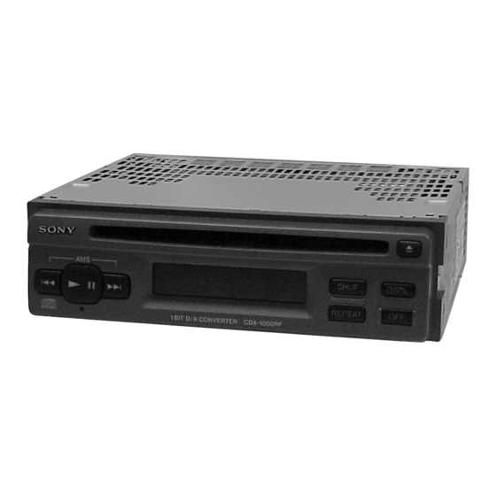
Sony CDX-1000RF Service Manual
Compact disc player
Hide thumbs
Also See for CDX-1000RF:
- Service manual (38 pages) ,
- Operating instructions (3 pages) ,
- Limited warranty (1 page)
Table of Contents
Advertisement
Quick Links
All manuals and user guides at all-guides.com
SERVICE MANUAL
SPECIFICATIONS
AUDIO POWER SPECIFICATIONS
POWER OUTPUT AND TOTAL HARMONIC DISTORTION
13 watts per channel minimum continuous average power into
4 ohms, 4 channels driven from 20 Hz to 20 kHz with no more
than 1% total harmonic distortion.
Other Specifications
CD player section
System
Compact disc digital audio
system
Signal-to-noise ratio
90 dB
Frequency response
10 – 20,000 Hz
Wow and flutter
Below measurable limit
Laser Diode Properties
Material
GaAs+GaAlAs
Wavelength
785 – 815 nm (Typ. 800 nm)
Emission Duration
Continuous
Laser output power
Less than 0.5 mW*
* This output is the value measured at a distance
of 0.7 mm from the objective lens surface on the
Optical Pick-up Block.
CDX-1000RF
Model Name Using Similar Mechanism
CD Drive Mechanism Type
Optical Pick-up Name
General
Outputs
Power requirements
Current drain
Dimensions
Mounting dimensions
Mass
Supplied accessories
Design and specifications are subject to change without
notice.
COMPACT DISC PLAYER
US Model
CDX-2500R
MG-363X-121
KSS-521A
Line outputs
12 V DC car battery
(negative ground)
2A (at disc loading)
Approx. 178 × 50 × 173 mm
× 2 × 6
(7
in.)
1/8
7/8
(w/h/d)
Approx. 182 × 53 × 159 mm
× 2
× 6
(7
in.)
1/4
1/8
3/8
(w/h/d)
Approx. 1.1 kg (2 lb. 7 oz.)
Parts for installation and
connections (1 set)
1
Advertisement
Table of Contents

Related Manuals for Sony CDX-1000RF


Summary of Contents for Sony CDX-1000RF
- Page 1 All manuals and user guides at all-guides.com CDX-1000RF SERVICE MANUAL US Model Model Name Using Similar Mechanism CDX-2500R CD Drive Mechanism Type MG-363X-121 SPECIFICATIONS Optical Pick-up Name KSS-521A AUDIO POWER SPECIFICATIONS POWER OUTPUT AND TOTAL HARMONIC DISTORTION 13 watts per channel minimum continuous average power into 4 ohms, 4 channels driven from 20 Hz to 20 kHz with no more than 1% total harmonic distortion.
-
Page 2: Table Of Contents
5-4. CD Mechanism Section (2) ..........29 THE PARTS LIST ARE CRITICAL TO SAFE OPERATION. 5-5. CD Mechanism Section (3) ..........30 REPLACE THESE COMPONENTS WITH SONY PARTS WHOSE PART NUMBERS APPEAR AS SHOWN IN THIS MANUAL OR 6. ELECTRICAL PARTS LIST ........ - Page 3 All manuals and user guides at all-guides.com SECTION 1 GENERAL This section is extracted from instruction manual.
- Page 4 All manuals and user guides at all-guides.com...
-
Page 5: Panel Assy, Front
All manuals and user guides at all-guides.com SECTION 2 DISASSEMBLY Note : Follow the disassembly procedure in the numerical order given. 2-1. PANEL ASSY, FRONT 3 claw 2 claws 1 claws 4 CNP801 5 panel assy, front 2-2. CD MECHANISM BLOCK 2 PTT 2.6x6 7 PTT 2.6x6 8 bracket (M/D) -
Page 6: Main Board
All manuals and user guides at all-guides.com 2-3. MAIN BOARD 6 MAIN board 5 ground point screw 4 ground point screws (PTT 2.6x6) (PTT 2.6x6) 3 PTT 2.6x6 2 PTT 2.6x6 1 PTT 2.6x6 2-4. CHASSIS (REAR) 4 chassis (rear) 3 PTT 2.6x6 2 PTT 2.6x6 1 PTT 2.6x6... -
Page 7: Chassis (T) Sub Assy
All manuals and user guides at all-guides.com 2-5. CHASSIS (T) SUB ASSY 4 P 2x3 3 P 2x3 5 chassis (T) sub assy 1 Unsolder the lead wires. 2 P 2x3 white black 2-6. LEVER ASSY 5 guide (disc) 6 lever (R) assy 3 tension spring (LR) 7 lever (L) assy 1 PS 2x4... -
Page 8: Servo Board
All manuals and user guides at all-guides.com 2-7. SERVO BOARD 8 PS 2x4 7 PS 2x4 2 CN2 3 Removal the solders. 1 CN3 5 P 2x3 9 SERVO board 4 Removal the solders. 6 loading motor assy 2-8. ROLLER ASSY •... -
Page 9: Chassis (Op) (O/S) Assy
All manuals and user guides at all-guides.com 2-9. CHASSIS (OP) (O/S) ASSY 7 chassis (OP) (O/S) assy 8 compression spring (FL) 1 tension spring (KF1) 9 compression spring (FL) 2 tension spring (KR1) 5 Fit lever (D) in the direction of the arrow. 6 Turn loading ring in the direction of the arrow. -
Page 10: Electrical Adjustments
All manuals and user guides at all-guides.com SECTION 3 ELECTRICAL ADJUSTMENTS CD SECTION Focus Gain Adjustment (Coarse adjustment) This adjustment is not required unless the following parts are replaced: • Optical pick-up Note: • 1. CD Block basically constructed to operate without adjustment. Therefore, check each item in order given. -
Page 11: Diagrams
All manuals and user guides at all-guides.com SECTION 4 DIAGRAMS 4-1. IC PIN DESCRIPTION • IC801 µPD17705GC-547-3B9 (SYSTEM CONTROL) Pin No. Pin Name Pin Description Pin No. Pin Name Pin Description — Not used. (Connect to ground in this set.) CD_RST Reset output to CD signal processor IC. -
Page 12: Block Diagram -Cd Section (1/2)
All manuals and user guides at all-guides.com CDX-1000RF 4-2. BLOCK DIAGRAM — CD SECTION (1/2) — OPTICAL PICK-UP RF AMP, SERVO CONTROL DIGITAL SIGNAL PROCESSOR D/A CONVERTER KSS-521A IC701 RF 0 PCMD VOUTL CD L-CH SECTION (2/2) CLKO BCKIN VOUTR... -
Page 13: Block Diagram -Cd Section (2/2)
All manuals and user guides at all-guides.com CDX-1000R 4-3. BLOCK DIAGRAM — CD SECTION (2/2) — (Page 12) ELECTRONIC VOLUME SECTION IC401 (1/2) CD L-CH PJ401 AUDIO OUT CD R-CH MUTE VOLUME LEVEL Q401 CONTROL CONTROL VOLUME CONTROL LEVEL CONTROL DEVIATION CNJ601 L101... -
Page 14: Block Diagram -Display, Power Supply Section
All manuals and user guides at all-guides.com CDX-1000RF 4-4. BLOCK DIAGRAM — DISPLAY, POWER SUPPLY SECTION — LIQUID CRYSTAL DISPLAY PANEL SYSTEM CONTROL LCD DRIVER LCD851 IC801 (3/3) IC851 RESET LCD_DAT DATA COM1 LCD_CLK COM2 S881 LCD_CE (RESET) LCD_INH •... -
Page 15: Circuit Boards Location
All manuals and user guides at all-guides.com 4-5. CIRCUIT BOARDS LOCATION • Waveforms (MODE:PLAY) THIS NOTE IS COMMON FOR PRINTED WIRING BOARDS AND SCHEMATIC DIAGRAMS. (In addition to this, the necessary note is printed in each block.) for schematic diagram: •... -
Page 16: Printed Wiring Boards -Cd Mechanism Section
All manuals and user guides at all-guides.com CDX-1000RF 4-6. PRINTED WIRING BOARDS — CD MECHANISM SECTION — • Refer to page 15 for Circuit Boards Location. • Semiconductor Location Ref. No. Location (Page 18) -
Page 17: Schematic Diagram -Cd Mechanism Section
All manuals and user guides at all-guides.com CDX-1000R 4-7. SCHEMATIC DIAGRAM — CD MECHANISM SECTION — • Refer to page 15 for Waveforms. • Refer to page 23 for IC Block Diagrams. (Pag Note: • Voltage and waveforms are dc with respect to ground under no-signal conditions. -
Page 18: Printed Wiring Board -Main Section
All manuals and user guides at all-guides.com CDX-1000RF 4-8. PRINTED WIRING BOARD — MAIN SECTION — • Refer to page 15 for Circuit Boards Location. • Semiconductor Location Ref. No. Location F-13 F-11 D401 D402 D901 D902 D903 D904 D905... -
Page 19: Schematic Diagram -Main Section (1/2)
All manuals and user guides at all-guides.com CDX-1000R 4-9. SCHEMATIC DIAGRAM — MAIN SECTION (1/2) — • Refer to page 21 for Waveforms. • Refer to page 25 for IC Block Diagrams. (Page 17) (Page 20) (Page 21) Note: • Voltage is dc with respect t ground under no-signal condition. -
Page 20: Schematic Diagram -Main Section (2/2)
All manuals and user guides at all-guides.com CDX-1000RF 4-10. SCHEMATIC DIAGRAM — MAIN SECTION (2/2) — • Refer to page 21 for Waveforms. • Refer to page 25 for IC Block Diagrams. (Page 19) Note: • Voltage is dc with respect to ground under no-signal condition. -
Page 21: Schematic Diagram -Display Section
All manuals and user guides at all-guides.com CDX-1000R 4-11. SCHEMATIC DIAGRAM — DISPLAY SECTION — • Waveforms (MODE:PLAY) 5.1Vp-p 22.7µsec IC701 (LRCIN) (Page 19) 5.1Vp-p 474nsec (BCKIN) IC701 4.7Vp-p 16.9344MHz (XTO) IC701 4Vp-p 16.89MHz (CLKO) IC701 2.7Vp-p 4.5MHz (XOUT) IC801 4.1Vp-p 22.7µsec (OSC) -
Page 22: Printed Wiring Board -Display Section
All manuals and user guides at all-guides.com CDX-1000RF 4-12. PRINTED WIRING BOARD — DISPLAY SECTION — • Refer to page 15 for Circuit Boards Location. (Page 18) • Semiconductor Location Ref. No. Location D851 D861 D862 D863 D864 D865 B-11... - Page 23 All manuals and user guides at all-guides.com • IC Block Diagrams IC1 CXD2507AQ (SERVO Board) SERVO AUTO DATA SEQUENCER XRST SENS SUB CODE MUTE PROCESSOR INTERFACE SQCK DIGITAL LOCK SQSO TEST EXCK SBSO FILO SCOR DIGITAL FILI DEMODULATOR WFCK EMPH AVSS CLTV ASYMMETRY...
- Page 24 All manuals and user guides at all-guides.com IC2 CXA1782BQ 27 26 25 LEVEL S MIRR SENS RF IV AMP1 DFCT C.OUT XRST RF IV AMP2 FE BIAS IIL DATA REGISTER INPUT SHIFT REGISTER DATA ADDRESS DECODER OUTPUT DECODER TOG1-3 FS1-4 TG1-2 TM1-7 PS1-4...
- Page 25 All manuals and user guides at all-guides.com IC1 BA1405F-E2 (MAIN Board) 17 16 15 13 12 11 10 BUFFER BUFFER OSC 38kHz 5 6 7 8 IC401 BA4558F OUT1 –IN1 OUT2 +IN1 –IN2 +IN2 IC701 PCM1717E-S DGND CONTROL CLKO LRCIN ML/MUTE INPUT INTERFACE...
-
Page 26: Exploded Views
All manuals and user guides at all-guides.com SECTION 5 EXPLODED VIEWS NOTE: • The mechanical parts with no reference • Color Indication of Appearance Parts The components identified by number in the exploded views are not supplied. mark 0 or dotted line with mark Example : •... -
Page 27: Front Panel Section
All manuals and user guides at all-guides.com 5-2. FRONT PANEL SECTION LCD851 Ref. No. Part No. Description Remark Ref. No. Part No. Description Remark 3-043-188-01 BUTTON (PLAY) * 56 3-043-193-01 PLATE (LCD), GROUND X-3378-481-1 PANEL ASSY, FRONT * 57 3-043-196-01 SHEET (D) 3-043-190-01 BUTTON (AMS) * 58 X-3378-707-1 HOLDER (LCD) ASSY... -
Page 28: Cd Mechanism Section (1)
All manuals and user guides at all-guides.com 5-3. CD MECHANISM SECTION (1) (MG-363X-121) M903 Ref. No. Part No. Description Remark Ref. No. Part No. Description Remark * 101 1-659-836-11 DISC IN SW BOARD 3-017-301-01 ARM (ROLLER) * 102 A-3291-816-B CHASSIS (T) SUB ASSY 3-936-756-01 ROLLER (D) 3-931-909-01 SPRING (LR), TENSION 3-321-393-01 WASHER, STOPPER... -
Page 29: Cd Mechanism Section (2)
All manuals and user guides at all-guides.com 5-4. CD MECHANISM SECTION (2) (MG-363X-121) Ref. No. Part No. Description Remark Ref. No. Part No. Description Remark 3-931-893-01 ARM, CHUCKING A-3277-802-C CHASSIS (M) COMPLETE ASSY 3-931-897-01 DAMPER (T) 3-931-883-01 SPRING (TR), TENSION 3-931-879-02 LEVER (D) 3-931-881-01 LEVER (LOCK) * 154... -
Page 30: Cd Mechanism Section (3)
All manuals and user guides at all-guides.com 5-5. CD MECHANISM SECTION (3) (MG-363X-121) M901 M902 The components identified by mark 0 or dotted line with mark 0 are critical for safety. Replace only with part number specified. Ref. No. Part No. Description Remark Ref. -
Page 31: Electrical Parts List
All manuals and user guides at all-guides.com SECTION 6 ELECTRICAL PARTS LIST DISC IN SW DISPLAY NOTE: • Due to standardization, replacements in • Items marked “*” are not stocked since The components identified by mark 0 or dotted line with mark the parts list may be different from the they are seldom required for routine service. - Page 32 All manuals and user guides at all-guides.com LIMIT SW LOAD SW MAIN Ref. No. Part No. Description Remark Ref. No. Part No. Description Remark 1-659-835-12 LIMIT SW BOARD 1-126-160-11 ELECT *************** 1-164-346-11 CERAMIC CHIP 1-164-346-11 CERAMIC CHIP < SWITCH > 1-163-021-11 CERAMIC CHIP 0.01uF 1-124-233-11 ELECT...
- Page 33 All manuals and user guides at all-guides.com MAIN Ref. No. Part No. Description Remark Ref. No. Part No. Description Remark < JACK > L101 1-235-778-21 FILTER, LOW PASS L201 1-235-778-21 FILTER, LOW PASS CNJ600 1-793-598-11 JACK (ANTENNA IN) L801 1-410-501-11 INDUCTOR 2.2uH L901 1-416-539-11 INDUCTOR...
- Page 34 All manuals and user guides at all-guides.com MAIN Ref. No. Part No. Description Remark Ref. No. Part No. Description Remark 1-216-063-11 RES-CHIP 3.9K 1/10W R332 1-216-049-11 RES-CHIP 1/10W 1-216-073-00 METAL CHIP 1/10W R333 1-216-073-00 METAL CHIP 1/10W 1-216-073-00 METAL CHIP 1/10W R401 1-216-049-11 RES-CHIP...
- Page 35 All manuals and user guides at all-guides.com MAIN SERVO Ref. No. Part No. Description Remark Ref. No. Part No. Description Remark < VARIABLE RESISTOR > 1-109-982-11 CERAMIC CHIP 1-163-021-11 CERAMIC CHIP 0.01uF RV10 1-241-761-11 RES, ADJ, CARBON 1K 1-164-004-11 CERAMIC CHIP 0.1uF RV11 1-238-019-11 RES, ADJ, CARBON 47K...
- Page 36 All manuals and user guides at all-guides.com SERVO Ref. No. Part No. Description Remark Ref. No. Part No. Description Remark JR35 1-216-296-00 SHORT 1-216-097-11 RES-CHIP 100K 1/10W JR36 1-216-296-00 SHORT 1-216-117-00 METAL CHIP 680K 1/10W JR37 1-216-296-00 SHORT 1-216-109-00 METAL CHIP 330K 1/10W JR38...
- Page 37 All manuals and user guides at all-guides.com Ref. No. Part No. Description Remark ************** HARDWARE LIST ************** 7-685-792-09 SCREW +PTT 2.6X6 (S) 7-685-105-19 SCREW +P 2X8 TYPE2 NON-SLIT 7-628-253-00 SCREW +PS 2X4 7-627-553-37 SCREW, PRECISION +P 2X3 TYPE3 7-627-553-17 SCREW, PRECISION +P 2X2 TYPE3 7-627-000-00 SCREW, PRECISION +P 1.7X2.2 TYPE3 7-627-850-28 SCREW, PRECISION +P 1.4X3 *************************************************************...
- Page 38 All manuals and user guides at all-guides.com CDX-1000RF Sony Corporation 9-870-139-11 2000C0416-1 Mobile Electronics Division Company Printed in Japan ©2000. 3 Published by General Engineering Dept.