Sony GTK-XB5 Service Manual
Hide thumbs
Also See for GTK-XB5:
- Operating instructions manual (32 pages) ,
- Operating instruction (91 pages)
Table of Contents
Advertisement
SERVICE MANUAL
Ver. 1.4 2017.02
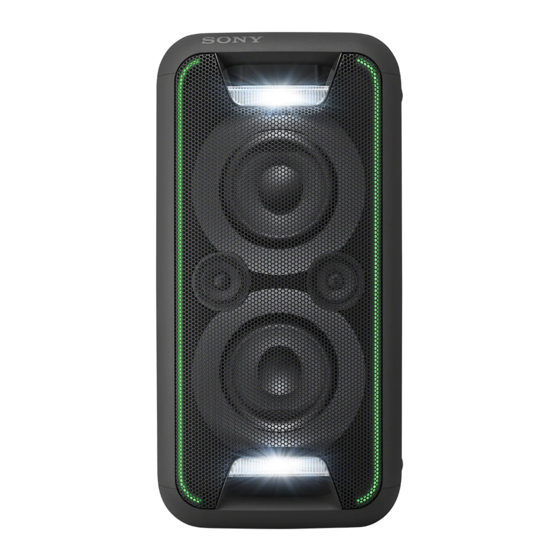
Speaker section
Tweeter:
50 mm (2 in) × 2, cone type
Woofer:
130 mm (5
in) × 2, cone type
Inputs
AUDIO/PARTY CHAIN IN L/R:
Voltage 2 V, impedance 10 kilohms
Outputs
AUDIO/PARTY CHAIN OUT L/R:
Voltage 2 V, impedance 600 ohms
9-896-299-05
2017B33-1
Sony Video & Sound Products Inc.
©
2017.02
SPECIFICATIONS
BLUETOOTH section
Communication system:
BLUETOOTH Standard version 3.0
Output:
BLUETOOTH Standard Power Class 2
Maximum communication range:
Line of sight approx. 10 m (33 feet)
Frequency band:
2.4 GHz band (2.4000 GHz –
2.4835 GHz)
Modulation method:
FHSS (Freq Hopping Spread
Spectrum)
Compatible BLUETOOTH profiles
2)
:
A2DP (Advanced Audio Distribution
Profile)
AVRCP (Audio Video Remote Control
Profile)
SPP (Serial Port Profile)
Supported codecs:
SBC (Sub Band Codec)
AAC (Advanced Audio Coding)
LDAC
1)
The actual range will vary depending
on factors such as obstacles between
devices, magnetic fields around a
microwave oven, static electricity,
reception sensitivity, antenna's
performance, operating system, software
application, etc.
2)
BLUETOOTH standard profiles indicate the
purpose of BLUETOOTH communication
between devices.
GTK-XB5
Canadian Model
Australian Model
General
Power requirements:
North American model: AC 120 V,
60 Hz
Taiwan model: AC 120 V,
50/60 Hz
Korean model: AC 220 V
1)
50/60 Hz
Other models: AC 120 V
50/60 Hz
Power consumption:
30 W
Standby power consumption:
When BLUETOOTH standby mode is
set to off: 0.5 W (eco mode)
When BLUETOOTH standby mode is
set to on: 2.8 W (all wireless network
ports on)
Dimensions (W/H/D) (Approx.):
262 mm × 524 mm × 273 mm
(10
in × 20
in × 10
Mass (Approx.):
7 kg (15 lb 7 oz)
Quantity of the system:
1 piece
Supplied accessories:
AC power cord (1)
AC plug adaptor* (1) (E4, SP6, LA)
* This plug adaptor is not for the use
in Chile, Paraguay and Uruguay. Use
this plug adaptor in the countries
where it is necessary.
Design and specifications are subject to
change without notice.
HOME AUDIO SYSTEM
US Model
AEP Model
UK Model
E Model
–
240 V,
–
240 V,
in)
Advertisement
Table of Contents

Related Manuals for Sony GTK-XB5


Summary of Contents for Sony GTK-XB5
- Page 1 BLUETOOTH standard profiles indicate the this plug adaptor in the countries purpose of BLUETOOTH communication where it is necessary. between devices. Design and specifications are subject to change without notice. HOME AUDIO SYSTEM 9-896-299-05 2017B33-1 Sony Video & Sound Products Inc. © 2017.02...
- Page 2 LES DIAGRAMMES SCHÉMATIQUES ET LA LISTE DES PIÈCES SONT CRITIQUES POUR LA SÉCURITÉ DE FONC- TIONNEMENT. NE REMPLACER CES COMPOSANTS QUE PAR DES PIÈCES SONY DONT LES NUMÉROS SONT DON- NÉS DANS CE MANUEL OU DANS LES SUPPLÉMENTS PUBLIÉS PAR SONY.
-
Page 3: Table Of Contents
GTK-XB5 TABLE OF CONTENTS SERVICING NOTES 4-11. Schematic Diagram - CONTROL Board - ...... 31 ..........4-12. Printed Wiring Board - FLASH LED Board - ....32 4-13. Schematic Diagram - FLASH LED Board - ....32 DISASSEMBLY 4-14. Printed Wiring Board - NFC Board - ......33 2-1. - Page 4 GTK-XB5 Ver. 1.4 SECTION 1 SERVICING NOTES The SERVICING NOTES contains important information for servicing. Be sure to read this section before repairing the unit. UNLEADED SOLDER MODEL IDENTIFICATION Boards requiring use of unleaded solder are printed with the lead- Distinguish by Part No.
-
Page 5: Disassembly
GTK-XB5 SECTION 2 DISASSEMBLY • This set can be disassembled in the order shown below. 2-1. DISASSEMBLY FLOW 2-2. TOP COVER BLOCK (Page 6) 2-6. RIGHT SIDE PANEL, 2-3. MAIN BOARD LEFT SIDE PANEL (Page 7) (Page 10) 2-4. POWER BOARD (Page 8) 2-7. -
Page 6: Top Cover Block
GTK-XB5 Note: Follow the disassembly procedure in the numerical order given. 2-2. TOP COVER BLOCK Note 1: When removing the rubber (circle), insert a sharp-tipped object such as 2 rubber (circle) tweezers into the cutout. 4 two rubbers 5 screw (small circle) tweezers, etc. -
Page 7: Main Board
GTK-XB5 2-3. MAIN BOARD Note 1: When replacing the MAIN board, be sure to replace the MAIN board and the NFC board simultaneously. The MAIN board cannot replace with single. Among the repair parts, the MAIN board and the NFC board are supplied as one unit. -
Page 8: Power Board
GTK-XB5 2-4. POWER BOARD 3 two screws 3 two screws hole 5 POWER board Note 1: When installing the POWER board, align the claw and hole. 4 Remove the POWER board in the direction of the arrow. 1 connector (XP1) -
Page 9: Nfc Board, Control Board
GTK-XB5 2-5. NFC BOARD, CONTROL BOARD Note 1: When replacing the NFC board, be sure to replace the MAIN board and the NFC board simultaneously. The NFC board cannot replace with single. Among the repair parts, the MAIN board and the NFC board are supplied as one unit. -
Page 10: Right Side Panel, Left Side Panel
GTK-XB5 2-6. RIGHT SIDE PANEL, LEFT SIDE PANEL 4 right side panel Note 1: When installing the right side panel, remove the used bond and use a new bond to fix the right side panel. bond 1 rubber top side... -
Page 11: Metal Case Block
GTK-XB5 2-7. METAL CASE BLOCK 2 woofer cable 1 FFC cable connector (XP10) (9P MAIN BD-FA BD) tting (XP17) 3 tweeter cable FFC cable front side connector (XP13) (9P MAIN BD-FA BD) BT board – – Note: Be careful not to damage the BT board. -
Page 12: Bottom Cover + Plate
GTK-XB5 2-8. BOTTOM COVER + PLATE top side 1 two handle rubbers front side 2 two screws bottom side Note 1: When removing the bottom cover + plate, move the bottom cover + plate slowly and remove the bond as shown figure. -
Page 13: Front Panel Block-1
GTK-XB5 2-9. FRONT PANEL BLOCK-1 • Continued on 2-10 (page 14). 1 two screws front panel block bottom side speaker cabinet 1 four screws front panel block rear side top side about boss 3 to 5 mm total eight bosses... -
Page 14: Front Panel Block-2
GTK-XB5 2-10. FRONT PANEL BLOCK-2 1 Insert a thick screwdriver into the left side Note 1: Make sure to proceed with the top and bottom sides and widen the gap (perform at two places). first because the right and left sides may damage Note 2: Be careful because if a screwdriver is the sides of the front panel block. -
Page 15: Speaker Led (Top) Board, Flash Led Board
GTK-XB5 2-11. SPEAKER LED (TOP) BOARD, FLASH LED BOARD boss top side 3 Remove the FLASH LED board block in the direction of the arrow. front panel block 7 connector (XP61) 5 TUBE LED board cable connector (XP67) 4 TUBE LED LEFT board cable... -
Page 16: Tube Led Right Board, Tube Led Left Board
GTK-XB5 2-12. TUBE LED RIGHT BOARD, TUBE LED LEFT BOARD top side front panel block 3 TUBE LED LEFT board 2 tube PCBA bracket (left) 1 screw front side 3 TUBE LED RIGHT board 2 tube PCBA bracket (right) 1 screw 2-13. -
Page 17: Speaker Unit (Tw) (Sp3, Sp4)
GTK-XB5 2-14. SPEAKER UNIT (TW) (SP3, SP4) Cable (4P tweeter SP line) setting cable cable cable (4P tweeter SP line) (4P tweeter SP line) (4P tweeter SP line) groove groove groove – Sectional view – – Sectional view – – Sectional view –... -
Page 18: Speaker Unit (Wf) (Sp1, Sp2)
GTK-XB5 2-15. SPEAKER UNIT (WF) (SP1, SP2) Note 2: When installing the woofer cable, make the position of caulking of terminals is outside. top side terminal (wide) right side top side left side woofer cable terminal (narrow) front side [red line]... -
Page 19: Test Mode
GTK-XB5 SECTION 3 TEST MODE SOFTWARE VERSION It can check the information of current software version. Procedure: 1. Press the [ ] button to turn the power on. 2. Press two buttons of the [FUNCTION] and [LIGHT] simulta- neously for 5 seconds. -
Page 20: Diagrams
GTK-XB5 SECTION 4 DIAGRAMS 4-1. BLOCK DIAGRAM AK4430 Audio Out/Party Chain MCLK1 BCLK1 AK5358 DATA3 BTL 100W*2(6 ) 30% Audio IN LRCLK1 01UKOKAD A-101 DATA1 MCLK1 BCLK1 PWM1 LRCLK1 Audio Processor AMP IC YSS952 TAS5534 TAS5342A BCLK0 PWM2 LRCLK0 DATA2... - Page 21 GTK-XB5 THIS NOTE IS COMMON FOR PRINTED WIRING BOARDS AND SCHEMATIC DIAGRAMS. • Circuit Boards Location (In addition to this, the necessary note is printed in each block.) For Printed Wiring Boards. For Schematic Diagrams. MAIN board NFC board Note:...
-
Page 22: Printed Wiring Board - Main Board
GTK-XB5 4-2. PRINTED WIRING BOARD - MAIN Board - • See page 21 for Circuit Boards Location. • : Uses unleaded solder. MAIN BOARD (COMPONENT SIDE) MAIN BOARD (CONDUCTOR SIDE) GTK-XB5... -
Page 23: Schematic Diagram - Main Board (1/7)
GTK-XB5 4-3. SCHEMATIC DIAGRAM - MAIN Board (1/7) - MAIN BOARD (1/7) 0.1uF/50V/X7R 0.1uF/50V/X7R TPS54140 TPS54140 32V_MAIN STB_3V3 POWER INPUT 470pF/50V/NP0 470pF/50V/NP0 470pF/50V/NP0 470pF/50V/NP0 BOOT 120/2A 120/2A STB_5V FB17 FB17 120/2A 120/2A +12V COMP PSON VCC_D SS/TR VSNS SY8088 SY8088... -
Page 24: Schematic Diagram - Main Board (2/7)
GTK-XB5 4-4. SCHEMATIC DIAGRAM - MAIN Board (2/7) - MAIN BOARD (2/7) MCU_3V3 STB_3V3 Close to MCU FB48 FB48 4.7K 4.7K MCU_3V3 4.7K 4.7K C341 C341 C342 C342 C344 C344 C345 C345 C347 C347 To KEY Board XP16 XP16 FB40... -
Page 25: Schematic Diagram - Main Board (3/7)
GTK-XB5 4-5. SCHEMATIC DIAGRAM - MAIN Board (3/7) - MAIN BOARD (3/7) BT_BM63 BT_BM63 Apple Authentication TM11 TM11 BAT_IN TM12 TM12 Active Mode Current : 7.5mA BT_LRCK R103 R103 TM13 TM13 BT_LRCK RFS0 BT_BCLK R108 R108 BT_BCLK SCLK0 BT_DATA R110... -
Page 26: Schematic Diagram - Main Board (4/7)
GTK-XB5 4-6. SCHEMATIC DIAGRAM - MAIN Board (4/7) - MAIN BOARD (4/7) Audio IN Audio OUT Mute 3.3V_D1 STB_3V3 3.3V_D1 R182 R182 ADC_5V MUTE CE22 CE22 C149 C149 NC/PNP_3CG3906M NC/PNP_3CG3906M C119 C119 C172 C172 10uF/6.3V/X5R 10uF/6.3V/X5R FB22 FB22 10uF/6.3V/X5R 10uF/6.3V/X5R... -
Page 27: Schematic Diagram - Main Board (5/7)
GTK-XB5 4-7. SCHEMATIC DIAGRAM - MAIN Board (5/7) - MAIN BOARD (5/7) 1.8V_D 1.8V 3.3V_D1 3.3V AD_DATA R232 R232 Y_DATA_IN1 AD_DATA AD_LRCK R263 R263 Y_LRCLK_OUT AD_LRCK AD_MCLK R264 R264 Y_MCLK AD_MCLK AD_BCLK R265 R265 C205 C205 C141 C141 Y_BCLK_OUT C142... -
Page 28: Schematic Diagram - Main Board (6/7)
GTK-XB5 4-8. SCHEMATIC DIAGRAM - MAIN Board (6/7) - MAIN BOARD (6/7) AMP_3.3V TGND 3.3V_D1 AMP_3.3V C211 C211 C212 C212 PWM_HPM_L PWM_P_6 R308 R308 PWM_HPP_L PWM_M_6 0.1UF 0.1UF 0.1UF 0.1UF FB28 FB28 PWM_HPM_R PWM_P_5 C214 C214 4700pF 4700pF PWM_HPP_R PWM_M_5... -
Page 29: Schematic Diagram - Main Board (7/7)
GTK-XB5 4-9. SCHEMATIC DIAGRAM - MAIN Board (7/7) - MAIN BOARD (7/7) AMP_32V R358 R358 CE30 CE30 C291 C291 470uF/50V 470uF/50V 0.1uF/50V 0.1uF/50V C334 C334 V_12V 10NF 10NF R318 R318 C290 C290 R319 R319 0.1uF/50V 0.1uF/50V C289 C289 0.1uF/50V 0.1uF/50V... -
Page 30: Printed Wiring Board - Control Board
GTK-XB5 4-10. PRINTED WIRING BOARD - CONTROL Board - • See page 21 for Circuit Boards Location. • : Uses unleaded solder. CONTROL BOARD (COMPONENT SIDE) CONTROL BOARD (CONDUCTOR SIDE) GTK-XB5... -
Page 31: Schematic Diagram - Control Board
GTK-XB5 4-11. SCHEMATIC DIAGRAM - CONTROL Board - CONTROL BOARD To Main Board FB41 FB41 STB LED_5V R820 R820 MOLD WHITE_LED R840 R840 ADC_KEY21 ADC_KEY11 R818 R818 R WHITE_LED Power Power ESD7 ESD7 R815 R815 L WHITE_LED R828 R828 ADC_KEY11 1.48V... -
Page 32: Printed Wiring Board - Flash Led Board
GTK-XB5 4-12. PRINTED WIRING BOARD - FLASH LED Board - • See page 21 for Circuit Boards Location. • : Uses unleaded solder. FLASH LED BOARD (COMPONENT SIDE) FLASH LED BOARD (CONDUCTOR SIDE) 4-13. SCHEMATIC DIAGRAM - FLASH LED Board - FLASH LED BOARD 3.3V_D2... -
Page 33: Printed Wiring Board - Nfc Board
GTK-XB5 4-14. PRINTED WIRING BOARD - NFC Board - • See page 21 for Circuit Boards Location. 4-16. PRINTED WIRING BOARD - SPEAKER LED (TOP) Board - • See page 21 for Circuit Boards Location. • : Uses unleaded solder. -
Page 34: Printed Wiring Board - Tube Led Left Board
GTK-XB5 4-18. PRINTED WIRING BOARD - TUBE LED LEFT Board - • See page 21 for Circuit Boards Location. 4-20. PRINTED WIRING BOARD - TUBE LED RIGHT Board - • See page 21 for Circuit Boards Location. • : Uses unleaded solder. -
Page 35: Printed Wiring Board
GTK-XB5 4-22. PRINTED WIRING BOARD - SPEAKER LED (BTM) Board - • See page 21 for Circuit Boards Location. 4-24. PRINTED WIRING BOARD - TUBE LED Board - • See page 21 for Circuit Boards Location. • : Uses unleaded solder. -
Page 36: Schematic Diagram - Power Board
GTK-XB5 4-26. SCHEMATIC DIAGRAM - POWER Board - POWER BOARD R534 R534 R535 R535 CY503 CY503 470pF/250VAC 470pF/250VAC C508 C508 D505 D505 HER203 HER203 CY504 CY504 1000pF 1000pF 470pF/250VAC 470pF/250VAC R523 R523 8.2/2W 8.2/2W CE502 CE502 C502 C502 CE501 CE501... -
Page 37: Printed Wiring Board - Power Board
GTK-XB5 4-27. PRINTED WIRING BOARD - POWER Board - • See page 21 for Circuit Boards Location. • : Uses unleaded solder. POWER BOARD (COMPONENT SIDE) POWER BOARD (CONDUCTOR SIDE) -
Page 38: Exploded Views
GTK-XB5 Ver. 1.4 SECTION 5 EXPLODED VIEWS Note: • -XX and -X mean standardized parts, so • The mechanical parts with no reference • Color variations they may have some difference from the number in the exploded views are not sup-... -
Page 39: Side Panel Section
GTK-XB5 Ver. 1.4 5-2. SIDE PANEL SECTION cabinet section Ref. No. Part No. Description Remark Ref. No. Part No. Description Remark 9-885-212-22 LEFT SIDE PANEL (UC2 BLACK) (for BLACK) 9-885-212-20 RIGHT SIDE PANEL (UC2 BLACK) (for BLACK) (US, CND) (US, CND) -
Page 40: Cabinet Section
GTK-XB5 5-3. CABINET SECTION board section front panel section not supplied Ref. No. Part No. Description Remark Ref. No. Part No. Description Remark 9-885-212-29 HANDLE RUBBER (BLACK) (4 pieces, 1 set) 9-885-212-60 BOTTOM COVER (GREEN) + PLATE (for GREEN) (for BLACK) -
Page 41: Board Section
GTK-XB5 Ver. 1.4 5-4. BOARD SECTION (See Note) supplied not supplied Note: When replacing the MAIN board (Ref. No. 151), be sure to re- place the MAIN board and the NFC board (page 42) simultane- ously. The MAIN board cannot replace with single. Among the repair parts, the MAIN board and the NFC board are supplied as one unit. -
Page 42: Top Cover Section
GTK-XB5 5-5. TOP COVER SECTION not supplied Included in NFC board Ref. No. 151 (See Note) on page 41. not supplied FFC1 Note: When replacing the NFC board, be sure to replace the MAIN board (Ref. No. 151 on page 41) and the NFC board simultane- ously. -
Page 43: Front Panel Section
GTK-XB5 Ver. 1.4 5-6. FRONT PANEL SECTION • Rear side view not supplied not supplied not supplied not supplied FFC2 Ref. No. Part No. Description Remark Ref. No. Part No. Description Remark 9-885-212-69 SCREW M3X10 (30 pieces, 1 set) 9-885-212-50... -
Page 44: Accessories
GTK-XB5 Ver. 1.4 SECTION 6 ACCESSORIES Ref. No. Part No. Description Remark 4-597-264-11 MANUAL, INSTRUCTION (ENGLISH, FRENCH, SPANISH) (US, CND) 4-597-264-21 MANUAL, INSTRUCTION (ENGLISH) (UK, AUS) 4-597-264-31 MANUAL, INSTRUCTION (FRENCH, GERMAN, SPANISH, DUTCH, ITALIAN, POLISH) (AEP) 4-597-264-41 MANUAL, INSTRUCTION (RUSSIAN) (RU) - Page 45 GTK-XB5 MEMO...
- Page 46 GTK-XB5 REVISION HISTORY Ver. Date Description of Revision 2016.08 2016.09 Addition of RU, E4, E93, SP6 and LA models 2016.11 Addition of KR model 2017.01 Addition of AR model Deletion of Blue, Orange Red and Green color types (E4 and E93 models) (SMR-16039) 2017.02...