Advertisement
Quick Links
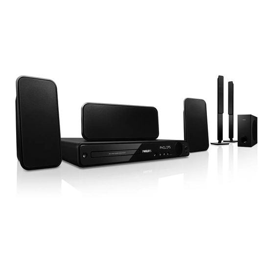
DVD Home Theatre System
Copyright 2009 Philips Consumer Electronics B.V. Eindhoven, The Netherlands
©
All rights reserved. No part of this publication may be reproduced, stored in a retrieval system or
transmitted, in any form or by any means, electronic, mechanical, photocopying, or otherwise
without the prior permission of Philips.
Published by
LM-SL0948
Service Audio Printed in The Netherlands Subject to modification
Version 1.1
TABLE OF CONTENTS
Location of PCB Boards ............................................ 1-2
Versions Variation ...................................................... 1-2
Specifications ............................................................ 1-3
Measurement Setup .................................................. 1-4
Service Aids .............................................................. 1-5
ESD & Safety Instruction .......................................... 1-6
Lead-free soldering Information ................................ 1-7
Setting procedure & Repair Instructions........................ 2
Disassembly Instructions & Service positions .............. 3
Block & Wiring Diagram ................................................ 4
DISP+LED+VOL Board.................................................. 5
MAIN Board.................................................................... 6
Power Board .................................................................. 7
MP3 IN Board ................................................................ 8
Scart Board .................................................................... 9
Mechanical Exploded View & Part List ........................ 10
Revision List ................................................................ 11
HTS3377
Chapter
/12/05/51
© 3141 785 33321
Advertisement

Related Manuals for Philips HTS3377/12


Summary of Contents for Philips HTS3377/12
- Page 1 Scart Board ..............9 Mechanical Exploded View & Part List ......10 Revision List ..............11 Copyright 2009 Philips Consumer Electronics B.V. Eindhoven, The Netherlands © All rights reserved. No part of this publication may be reproduced, stored in a retrieval system or transmitted, in any form or by any means, electronic, mechanical, photocopying, or otherwise without the prior permission of Philips.
- Page 2 1 - 2 LOCATION OF PCB BOARDS VERSION VARIATION: Type/Versions HTS3377 /12/05/51 Features Output Power - 1000W Voltage (220~240V) MP3 Link SERVICE SCENARIO MATRIX: HTS3377 Type/Versions Board in used /12/05/51 MAIN Board Power Board DISP+LED+VOL Board Scart Board MP3 IN Board *M = Module Level Repair...
- Page 3 1 - 3 SPECIFICATIONS Playback media Speakers DVD-Video, DVD+R/+RW, DVD-R/-RW, DVD+R DL, CD-R/ System ............full range satellite CD-RW, Audio CD, Video CD/SVCD, Picture CD, MP3-CD, Speaker impedance ... 4 ohm (centre), 4 ohm (Front/Rear) WMA-CD, DivX-CD, USB ash drive Speaker drivers .................
- Page 4 1 - 4 MEASUREMENT SETUP Tuner FM Bandpass LF Voltmeter 250Hz-15kHz e.g. PM2534 e.g. 7122 707 48001 RF Generator e.g. PM5326 S/N and distortion meter e.g. Sound Technology ST1700B Use a bandpass filter to eliminate hum (50Hz, 100Hz) and disturbance from the pilottone (19kHz, 38kHz). Use Audio Signal Disc SBC429 4822 397 30184 (replaces test disc 3)
- Page 5 1 - 5 SERVICE AIDS Service Tools: Universal Torx driver holder .........4822 395 91019 Torx bit T10 150mm ...........4822 395 50456 Torx driver set T6-T20 .........4822 395 50145 Torx driver T10 extended ........4822 395 50423 Compact Disc: SBC426/426A Test disc 5 + 5A ......4822 397 30096 SBC442 Audio Burn-in test disc 1kHz ....4822 397 30155 SBC429 Audio Signals disc .........4822 397 30184 Dolby Pro-logic Test Disc ........4822 395 10216...
- Page 6 1 - 6...
- Page 7 1 - 7...
- Page 8 In open mode, press “1“ “5“ “9“ on R/C the software upgrade? b) Press “ok” button to confi rm c) TV will show message as below: Cancel Current model HTS3377/12/05 Version: XX.XX.XX Release:XXXX.XX.XX f) Select “OK”, OSD will show: region Servo:XX.XX.XX.XX 8032:XX.XX.XX.XX...
- Page 9 2 - 2 2 - 2 REPAIR INSTRUCTIONS (ONE)
- Page 10 2 - 3 2 - 3 REPAIR INSTRUCTIONS (TWO)
- Page 11 2 - 4 2 - 4 REPAIR INSTRUCTIONS (THREE)
- Page 12 3 - 1 3 - 1 DISASSEMBLY INSTRUCTIONS Dismantling of the Front Panel Assemble 3) Loosen 6 screws and remove the Top Cover by lifting the rear portion upwards before sliding it out towards the rear. - 1 screw “A” each on the left & right side as shown in fi gure 4. 1) Open the DVD Tray by using the Open/Close Button while the Set is ON and disconnect the mains supply after removing the Tray - 4 screws “B”...
- Page 13 3 - 2 3 - 2 Dismantling of the DISP+LED+VOL&MP3 IN Board SERVICE POSITIONS 1) Loosen 10 screws “E” on the top of DISP+LED+VOL&MP3 IN Board as shown in fi gure 8. Service position A Figure 8 Dismantling of the Power Board 1) Loosen 4 screws “F”...
- Page 14 4 - 1 4 - 1 BLOCK DIAGRAM Sanyo / Sony pick up VF D Display AS A DVD Loader B+5V IC V 5888 V- CL K VF D DR IV ER V- CS V- DAT A PT6311 Loader motor driver KE Y 1080P 3.3V...
- Page 15 4 - 2 4 - 2 WIRING DIAGRAM...
- Page 16 5 - 1 5 - 1 FTD DISPLAY PIN ASSIGNMENT DISP+LED+VOL BOARD TABLE OF CONTENTS FTD Display Pin Assignment ............. 5-1 Circuit Diagram ................. 5-2 PCB Layout Top & Bottom View ............5-3 PIN CONNECTION...
- Page 17 5 - 2 5 - 2 CIRCUIT DIAGRAM C380 B1 C384 C1 C387 A2 C390 B2 C395 C4 DP351 A2 Q351 C1 R3051 B1 R3054 B1 R3057 C1 R3060 C1 R3063 B1 R3068 A3 R3072 C1 RB351 C4 RB357 C1 TA351 A1 TA354 C1 ZD310 C1...
- Page 18 5 - 3 5 - 3 PCB LAYOUT - TOP VIEW C386 C391 DP351 A2 ESD4 ESD6 J351 J353 J355 J357 J359 LD351 RB355 A1 RB357 B1 SN351 B3 TA352 TA354 VR351 A3 C389 C392 ESD1 ESD5 ESD7 J352 J354 J356 J358 J363...
-
Page 19: Table Of Contents
6 - 1 6 - 1 IN T ERN A L IC DIAGRAM - TAS5 5 0 8 B MAIN BOARD TABLE OF CONTENTS Internal IC Diagram ................6-1 Circuit Diagram(part one) ..............6-2 Circuit Diagram(part two) ..............6-3 Circuit Diagram(part three) ..............6-4 PCB Layout Top View ............... -
Page 20: Circuit Diagram(Part One)
6 - 2 6 - 2 CIRCUIT DIAGRAM - par t one C401 A1 R425 A1 Q402 A3 R4020 A3 C4013 A4 C4031 A4 C4043 A4 R488 A4 C410 B1 C421 B1 C4049 B2 R411 B2 R421 B2 C4054 B3 R4002 B3 R452 B3 R499 B3... -
Page 21: Circuit Diagram(Part Two)
6 - 3 6 - 3 CIRCUIT DIAGRAM - part two C0201 C2 C0214 C4 C0230 D1 C0248 B4 C104 A4 C208 A2 C223 D1 C236 A4 C261 D1 C718 B3 C737 A3 C812 A2 C827 B2 C840 B2 CE212 D1 CE807 D1 CN802 B1 FB205 C4... -
Page 22: Circuit Diagram(Part Three)
6 - 4 6 - 4 CIRCUIT DIAGRAM - part three C301 A1 C317 A3 C326 A1 C346 B3 C357 B1 C511 B4 C903 D1 C920 D1 CE302 D2 CE311 D2 CE320 D2 CE329 D3 FB312 B1 FE309 D3 JK302A B1 R3019 A2 R314 A1 R328 B2... -
Page 23: Pcb Layout Top View
6 - 5 6 - 5 PCB LAYOUT - TOP VIEW C317 JK701 A1 R711 C736 R254 R4018 A2 L416 C218 L201 R292 C331 R286 C342 R352 R722 C825 L501 R834 C912 R209 R601 IC404 C3 C4006 C4 C470 R433 R471 IC801 D1 R826... -
Page 24: Pcb Layout Bottom View
6 - 6 6 - 6 PCB LAYOUT - BOTTOM VIEW C0241 A1 R4030 A1 C4025 A2 D414 R4045 A2 C0603 A3 R4060 A3 C4000 B1 C485 C4001 B2 CE315 B2 C0230 B3 CE323 B3 C0246 B4 C728 FE301 B4 C506 C0215 C3 C236... - Page 25 7 - 1 7 - 1 INTERNAL IC DIAGRAM - AZ431 CATHODE POWER BOARD TABLE OF CONTENTS Internal IC Diagram ................7-1 Circuit Diagram .................. 7-2 ANODE PCB Layout Top View ............... 7-3 PCB Layout Bottom View ..............7-4...
- Page 26 7 - 2 7 - 2 CIRCUIT DIAGRAM BD901 A1 C910 D3 C923 D2 C936 B2 C947 C3 C957 A4 C965 C3 C974 B4 C985 B3 D904 B4 D915 C2 D927 C4 L901 C1 Q903 C3 Q913 A2 R906 C3 R916 A1 R926 C3 R935 B3...
- Page 27 7 - 3 7 - 3 PCB LAYOUT - TOP VIEW BD901 B1 C906 A3 C920 A2 C959 A3 C966 B4 C975 C4 CN906 C4 D917 B2 D927 B4 IC905 B4 J907 C2 J913 A4 J920 A4 J926 C4 L902 B1 NTC901 D1 R901 A4 R943 B2...
- Page 28 7 - 4 7 - 4 PCB LAYOUT - BOTTOM VIEW C907 B1 C928 A1 C938 A2 C947 B2 C955 B1 C967 B2 C983 B2 D904 B1 D928 B1 Q907 B1 R905 D4 R911 B1 R919 A1 R926 A2 R934 A3 R939 B2 R956 B1 R965 B2...
- Page 29 8 - 1 8 - 1 MP3 IN BOARD TABLE OF CONTENTS Circuit Diagram .................. 8-1 PCB Layout Top & Bottom View ............8-2...
- Page 30 8 - 2 8 - 2 CIRCUIT DIAGRAM C383 A3 FB351 A1 FB352 A1 FB355 A3 FB356 A3 FB357 A3 JK351 A2 R3079 A1 R3080 A1 RB352 A1 RB354 A2 USB351 A3 RB352 JK 351 FB 351 C383 MP3L USB 351 R 3079 RB354 FB 355...
- Page 31 8 - 3 8 - 3 PCB LAYOUT - TOP VIEW PCB LAYOUT - BOTTOM VIEW J360 J361 JK351 RB352 A1 RB354 A1 USB351 A2 C383 FB351 FB352 FB355 FB356 FB357 R3079 R3080...
- Page 32 9 - 1 9 - 1 SCART BOARD TABLE OF CONTENTS Circuit Diagram ................. 9-2 PCB Layout Scart PCB View ............. 9-3...
- Page 33 9 - 2 9 - 2 CIRCUIT DIAGRAM C710 C712 C714 FB707 B1 FB709 B1 FB711 A2 JK703 A2 R708 RB702 A1 C711 C713 C715 FB708 B1 FB710 A2 FB714 C2 R707 RB701 B1...
- Page 34 9 - 3 9 - 3 PCB LAYOUT - SCART PCB VIEW C710 C712 C714 FB707 A2 FB709 B3 FB711 A1 JK703 A2 R708 RB702 B1 C711 C713 C715 FB708 A1 FB710 A1 FB714 A1 R707 RB701 B3...
- Page 35 10 - 1 10 - 1 Mechanical Exploded View...
- Page 36 10 - 2 10 - 2 MECHANICAL & ACCESSORIES PARTS LIST Loc. 12NC Description MAIN UNIT 996510021087 VOLUME KNOB 996510021093 DISPLAY LENS 996510021077 DVD DOOR 996510021057 996510021057 FRONT PANEL /12/05 FRONT PANEL /12/05 996510021245 FRONT PANEL /51 996510010842 RUBBER FOOT 996510021068 FUNCTION KNOB 996510021069...
- Page 37 11 - 1 11 - 1 REVISION LIST Version 1.0 *Initial release Version 1.1 *P10-2 Loudspeaker System List updated. SPKC 996510021048 SPEAKER BOX - REAR LEFT (was SPEAKER BOX - CENTER) SPKRL 996510021052 SPEAKER BOX - REAR RIGHT (was SPEAKER BOX - REAR LEFT) SPKRR 996510021046 SPEAKER BOX - CENTER (was SPEAKER BOX - REAR RIGHT)