Advertisement
Quick Links
Service
Manual
1. MAIN UNIT & SPEAKERS
1.1
TECHNICAL SPECIFICATIONS ........................................................................... 1
1.2
WIRING DIAGRAM ............................................................................................... 3
1.3
BLOCK DIAGRAM ................................................................................................ 5
1.4
SCHEMATIC DIAGRAM AND PARTS LOCATION ............................................... 7
1.5
MICROPROSSESOR AND IC DATA .................................................................. 27
1.6
TECNICAL DESCRIPTION ................................................................................. 39
1.7
ADJUSTMENT PROCEDURE ............................................................................ 40
1.8
EXPLODED VIEW AND PARTS LIST ................................................................. 47
1.9
TAKING OUT THE DISC FOR EMERGENCY ................................................... 55
1.10 ELECTRICAL PARTS LIST ................................................................................. 50
2. DB-VLD210 (DVD Loader for MARANTZ)
3. DB-VPB210 / 211 / 212 / 213 / 214 / 215 (DVD PCB Module for MARANTZ)
Printed in Japan
All manuals and user guides at all-guides.com
POWER
SURROUND
ON/STANDBY
PHONES
MODE
BS
DVD
VIDEO
DIGITAL
TABLE OF CONTENTS
ER3000
OPEN/CLOSE
PLAY
STOP
PAUSE
PREV.
NEXT
MEMORY
MODE
F/P
TUNING
VOLUME
DOWN
UP
TV
FM/AM
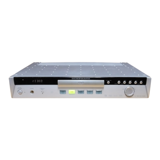
DVD RECEIVER ER3000
ER3000/
F1S
DVD Receiver
400K855010 AO
First Issue:2001.07
Advertisement

Related Manuals for Marantz ER3000


Summary of Contents for Marantz ER3000
- Page 1 TAKING OUT THE DISC FOR EMERGENCY ........... 55 1.10 ELECTRICAL PARTS LIST ................. 50 2. DB-VLD210 (DVD Loader for MARANTZ) 3. DB-VPB210 / 211 / 212 / 213 / 214 / 215 (DVD PCB Module for MARANTZ) ER3000 400K855010 AO First Issue:2001.07...
- Page 2 MARANTZ Parts for your equipment are generally available to our National Marantz Subsidiary or Agent. ORDERING PARTS : Parts can be ordered either by mail or by Fax.. In both cases, the correct part number has to be specified.
- Page 3 All manuals and user guides at all-guides.com 1.1 TECNICAL SPCIFICATIONS...
- Page 4 All manuals and user guides at all-guides.com...
- Page 5 All manuals and user guides at all-guides.com 1.2 WIRING DIAGRAM W801 AC CORD LIVE NEUTRAL W003 JG01 (25PIN FFC) J701 A-GND A-GND A-GND A-GND J801 Sub.W Sub.W +15V +15V -15V -15V +2.5V +2.5V -5VL -5VL U-COM & DSP PCB(PB01) +5VL +5VL RELAY RELAY...
- Page 6 All manuals and user guides at all-guides.com 1.3 BLOCK DIAGRAM STEREO CONTROL HEADPHONE FM AM TUNER UNIT PA01 MAIN AMP TUNER_OUT INDIVIDUAL & MASTER ELE.-VOL. X6CH PF04 PB01 TC9482 MAIN SUB-W FRONT INPUT SEL. FRONT 74HC4052 MAIN SUB-W SUB-W CENTER MAIN AK4527 MULTI CH.
- Page 7 All manuals and user guides at all-guides.com 1.4 SHEMATIC DIAGRAM AND PARTS LOCATION A002 FM/AM TUNER UNIT W002 YU15120503 TO TUNER JE03 AUDIO[15-0] -15V QJ09 A-GND A-GND DTA114YU RJ13 ↑ 100K ↑ ↑ ↑ ↑ +15V 1vrms CE13 CJ07 QJ04 0.015 AUDIO 0.01...
- Page 8 All manuals and user guides at all-guides.com 3V:COMPOSITE DOWNLOAD 0V:COMPONENT J604 J601 W001 YU28150503 TO DVD J607 TO VIDEO PCB(J202 VIA W007) R693 R668 +5VD VSELSW 6.8K R694 XMUTE XMUTE R667 R695 XRDY XRDY +5VD R696 SSCK Q620 SSCK AODAI AODAI DTC114EUA MUTE...
- Page 9 All manuals and user guides at all-guides.com C401 R401 R402 470/10V PC01 C402 R403 R404 R225 470/10V R237 +12VX R288 J402 R405 Q209 (3.0V) 6.8K C229 1.2K R226 DTC114EUA R270 0.01 C270 R289 J203 W008 J401 R271 3.3K 470/10V L215 BLM41P600S VIDEO SELECTOR C403...
- Page 10 All manuals and user guides at all-guides.com Q701 AUDIO AMPLIFIER TA2022-100 PA01 C730 PGND L705 C719 C720 100U R705 L701 C703 R703 10u/16V 6.8K BLM21A05PT D707 D708 → D703 R701 R732 RB160L-40 W003 J701 C701 +22V 160L-60 160L-60 100P 50V C721 →...
- Page 11 All manuals and user guides at all-guides.com W005 TO FRONT PCB (JY01 VIA W005) J805 PA01 Q815 PQ2TZ15u PGND J802 AC OUTLET R819 SWITCHED L808 LIVE AC100V G5PA-1 NEUTRAL MAX100W REGULATOR D816 ON:2.5V L804 +2.5V KDS121 L803 C834 1SS301 ON:3.3V 0.01 +3.3V SW-22V...
- Page 12 All manuals and user guides at all-guides.com W005 JY01 -20V -23V VY01 +5VL -24V FL DISPLAY +5VD +5VD QY04 RY05 DTC114EU HP-L HP-GND HP-R 10 11 12 13 14 15 16 23 24 25 26 27 28 29 30 31 32 33 34 35 36 37 38 41 42 DY11 SLR 342VC...
- Page 13 All manuals and user guides at all-guides.com JA03 FROM DVD PCB(A001) JA01 TO AUDIO PCB(J607 VIA W001) PJ01 CA02 470u/10V CA01 A003 470u/10V LOADER W011 A001 DVD PCB DVD UNIT JA04 TO VIDEO PCB(J201 VIA W006) JA02 FROM DVD PCB(A001) PJ01...
- Page 14 All manuals and user guides at all-guides.com Q808 Q702 QN05 QN02 Q741 Q807 Q901 QN01 QN04 QN03 Q806 Q805 Q818 Q812 Q820 Q804 Q810 Q819 PA01 Q817 Q803 Q816 Q802 Q821 Q811 Q801 Q809 Q814 Q813 Q902...
- Page 15 All manuals and user guides at all-guides.com QJ06 QK01 QJ05 Q303 Q302 QJ09 QJ08 QE07 QG02~QG18 Q618 Q614 Q601 QE02 QE03 QE01 QE04 Q611 Q613 Q610 Q607 QG01 QJ04 QJ51 QE06 Q608 Q612 Q617 Q616 Q606 Q609 Q605 Q620 Q619 QJ02 QJ03 QJ01 QJ07 Q301...
- Page 16 All manuals and user guides at all-guides.com Q239 Q241 Q233 Q236 Q203 Q219 Q232 Q215 Q235 Q202 Q238 Q218 Q231 Q237 Q217 Q243 Q240 PC01 Q214 Q230 Q234 Q201 Q245 Q207 Q209 Q211 Q210 Q216 Q242 Q244 PC02 PF03 PF04 PF02 QY04 QY01...
- Page 17 All manuals and user guides at all-guides.com PIN FUNCTION 1.5 MICROPROCESSOR AND IC DATA Pin No. Port Name Name Active Q605 :MB90F553A P20/A16 O A/D H(Analog) P21/A17 O TU-CL Tuner Pack (PLL:LC72131),RDS:LC72720 BLOCK DIAGRAM P22/A18 O TU-DO Tuner Pack (PLL:LC72131),RDS:LC72720 P23/A19 O TU-CE Tuner Pack (PLL:LC72131),RDS:LC72720...
- Page 18 All manuals and user guides at all-guides.com Q601 : LC89055W-RA8 BLOCK DIAGRAM PIN FUNCTION Pin name Function DISEL Data input pin (DIN0, DIN1) selection input pin DOUT Input bi-phase data through output pin DIN0 Digital data input pin (CMOS level, with pull-down resistance when no selected) DIN1 Digital data input pin (CMOS level, with pull-down resistance when no selected) DIN2...
- Page 19 All manuals and user guides at all-guides.com QK01 : AK4527 BLOCK DIAGRAM PIN FUNCTION Pin Name Function Audio SDOS SDTO Source Select Pin (Note 1) LIN+ "L": Internal ADC output, "H": DAUX input LIN- Control Mode Select Pin "L": 3-wire Serial, "H": I C Bus RIN+ SMUTE...
- Page 20 All manuals and user guides at all-guides.com Q701 : TA2022-100 Q609 : CS493292 BLOCK DIAGRAM BLOCK DIAGRAM PIN CONFIGURATION SCDIO, VBOOT2 DATA7:0, R/W, SCDOUT , VBOOT1 VN10 EMAD7:0, EMOE, EM WR, PSEL, ABOOT, EXTMEM, VPP1 VN10GND RESET GPIO7: 0 GPI O11 GPIO10 GPIO9 SCCLK...
- Page 21 All manuals and user guides at all-guides.com QG01 : TC9482F PIN FUNCTION PIN CONFIGURATION BLOCK DIAGRAM Q606 : AT24C04N BLOCK DIAGRAM PIN CONFIGURATION...
- Page 22 All manuals and user guides at all-guides.com QY01 : uPD16311GC-AB6 BLOCK DIAGRAM PIN FUNCTION Dimming Pin No. Symbol Pin Name Description Command decoder circuit Data input Inputs serial data at rising edge of shift clock, starting from lower bit. Data output Outputs serial data at falling edge of shift clock, starting from lower bit.
- Page 23 All manuals and user guides at all-guides.com 1.6 TECNICAL DESCRIPTION CLASS-T DIGITAL AUDIO AMPLIFIER TECHNOLOGY (TRIPATH) A Watershed in Digital Amplification Tripath amplifiers use a completely new proprietary method of Digital Power Processing“ that provides superior performance to conventional methods of amplification. For the first time, both high signal fidelity AND high power efficiency can be achieved with the same technology.
- Page 24 All manuals and user guides at all-guides.com 1.7 ADJUSTMENT PROCEDURE RS (Right Surround) , LS (Left Surround) , C (Ce nter) , SW (Sub Woofer) R (Front R ight) , L (Front Le ft) ..R720 ..R719 ..R760 ..
- Page 25 All manuals and user guides at all-guides.com R720, R719 R760, R759 R920, R919 RS, LS C, SW R, L...
- Page 26 All manuals and user guides at all-guides.com...
- Page 27 All manuals and user guides at all-guides.com...
- Page 28 All manuals and user guides at all-guides.com...
- Page 29 All manuals and user guides at all-guides.com Standby Push PAUSE+FM/AM Button And POWER Button Factory Mode1 Neutral Condition 0 MA Vxxxx Push POWER Button? Push FM/AM Push NEXT/PREV Push PAUSE+DVD Button Button Button TUNER TEST Mode No1-6 TEST Mode Region Check Push Push DVD Push POWER...
- Page 30 All manuals and user guides at all-guides.com 1.8 EXPLODED VIEW AND PARTS LIST 0 0 7 D x 6 5 1 2 8 0 3 8 G 9 3 8 G 2 X 4 ( A ) 5 1 2 8 T O P C O V E R A S S Y .
- Page 31 BNVTFCE1J101A TFCE1J101A TUNER UNIT AV01201140 FOR JAPAN W801 BJA2J049Z AC CORD F OR U *YC000520R NOT STANDARD SPARE PARTS A003 BJDDB-VLD210 DB-VLD210 DVD LOADER 402K304500 NOTE : "nsp" PART IS LISTED FOR REFERENCE ONLY, MARANTZ WILL NOT SUPPLY THESE PARTS.
- Page 32 SW01 VERS. POS. PART NO. DESCRIPTION COLOR (MJI) SW01 SW10NET NET ASS’Y (SW10) 400K202510 SW02 KA320LP185SOZ WOOFER UNIT (SW10) *QK000050R SW03 KJJ3N012 SPEAKER TERMINAL *YT002340R NOTE : "nsp" PART IS LISTED FOR REFERENCE ONLY, MARANTZ WILL NOT SUPPLY THESE PARTS.
- Page 33 NET HOLDER (LS100/LS100C) 400K259010 LS03 KAS1HK183SYZA TWEETER ASS’Y *QK000060R (LS100/LS100C) LS04 KAS9LP184SOZA WOOFER ASS’Y *QK000070R (LS100/LS100C) LS05 KSN1ALS100 NETWORK ASS’Y *ZZ001730R (LS100/LS100C) LS06 KJJ3N012 SPEAKER TERMINAL *YT002340R NOTE : "nsp" PART IS LISTED FOR REFERENCE ONLY, MARANTZ WILL NOT SUPPLY THESE PARTS.
- Page 34 KSA3A013Z LOOP ANTENNA 004Z KABAAM1.5V BATTERY R6P KR CP-2 005Z KJS4M011Y VIDEO CABLE (YELLOW) 2.0M 007Z KWX1A020 & SPEAKER CABLE KIT KWX1A021 011Z ATTACHED LABEL NOTE : "nsp" PART IS LISTED FOR REFERENCE ONLY, MARANTZ WILL NOT SUPPLY THESE PARTS.
- Page 35 All manuals and user guides at all-guides.com PACKING F L Y S H E E T 0 2 0 T 0 0 2 T 0 0 7 Z 0 1 1 Z U S E R G U I D E 0 0 7 S L A B E L 0 0 1 T...
- Page 36 All manuals and user guides at all-guides.com 1.9 TAKING OUT THE DISC FOR EMERGENCY 10. ELECTRICAL PARTS LIST NOTE ON SAFETY FOR FUSIBLE RESISTOR : ASSIGNMENT OF COMMON PARTS CODES. RESISTORS The suppliers and their type numbers of fusible resistors are as 1) GD05 x x x 140, Carbon film fixed resistor, 5% 1/4W follows ;...
- Page 37 1 F M 50V OA10505020 R703 KRJ10DJ102T CHIP 5% 1/16W NN05102610 C820 KCUS1H104ZF CER. CHIP 0.1 F F 50V DK98104300 R704 KRJ10DJ102T CHIP 5% 1/16W NN05102610 NOTE : "nsp" PART IS LISTED FOR REFERENCE ONLY, MARANTZ WILL NOT SUPPLY THESE PARTS.
- Page 38 CHIP 8.2k 5% 1/16W NN05822610 R934 KRJ10DJ473T CHIP 47k 5% 1/16W NN05473610 R772 KRJ10DJ102T CHIP 5% 1/16W NN05102610 R935 KRJ10DJ184T CHIP 180k 5% 1/16W NN05184610 NOTE : "nsp" PART IS LISTED FOR REFERENCE ONLY, MARANTZ WILL NOT SUPPLY THESE PARTS.
- Page 39 HZ20061210 L741 BLZ9J003Z BEAD FERRITE(CHIP) FC90020050 SBD 40V 1A BLM21A05PT D907 BVDRB160L60TE25 DIODE RB160L-60 TE25 *HZ200160R SBD 60V 1A L742 BLZ9J003Z BEAD FERRITE(CHIP) FC90020050 BLM21A05PT NOTE : "nsp" PART IS LISTED FOR REFERENCE ONLY, MARANTZ WILL NOT SUPPLY THESE PARTS.
- Page 40 CER. CHIP 1000pF 10% 50V DK96102300 RE07 KRJ10DJ473T CHIP 47k 5% 1/16W NN05473610 CJ33 KCUS1H181JC CHIP 180pF 5% 50V DD95181300 RE08 KRJ10DJ473T CHIP 47k 5% 1/16W NN05473610 NOTE : "nsp" PART IS LISTED FOR REFERENCE ONLY, MARANTZ WILL NOT SUPPLY THESE PARTS.
- Page 41 CHIP 4.7k 5% 1/16W NN05472610 R664 KRJ10DJ472T CHIP 4.7k 5% 1/16W NN05472610 R665 KRJ10DJ103T CHIP 10k 5% 1/16W NN05103610 R666 KRJ10DJ103T CHIP 10k 5% 1/16W NN05103610 NOTE : "nsp" PART IS LISTED FOR REFERENCE ONLY, MARANTZ WILL NOT SUPPLY THESE PARTS.
- Page 42 CER. CHIP 0.01 F 10% 50V DK96103300 AT24C04N-10SI-2.5 C260 KCEA1HH1R0T ELECT 1 F 50V OA10505020 Q609 BVICS493292 IC DSP CS493292 HC10009880 C262 KCUS1H103KB CER. CHIP 0.01 F 10% 50V DK96103300 NOTE : "nsp" PART IS LISTED FOR REFERENCE ONLY, MARANTZ WILL NOT SUPPLY THESE PARTS.
- Page 43 CHIP 100 5% 1/16W NN05101610 EL0405RA-470 R271 KRJ10DJ750T CHIP 5% 1/16W NN05750610 L213 KLQ470J405T COIL PEAKING(RADIAL) LC14733900 R274 KRJ10DJ101T CHIP 100 5% 1/16W NN05101610 EL0405RA-470 NOTE : "nsp" PART IS LISTED FOR REFERENCE ONLY, MARANTZ WILL NOT SUPPLY THESE PARTS.
- Page 44 YU08080500 W006 KWC1C4A14B100A FFC (JA04-J201) 14P X 100mm YU14100500 W007 KWC1C4A12B060A FFC (J202-J604) 12P X 60mm YU12060500 W008 KWC1C4A12B060A FFC (J203-J401) 12P X 60mm YU12060500 NOTE : "nsp" PART IS LISTED FOR REFERENCE ONLY, MARANTZ WILL NOT SUPPLY THESE PARTS.
- Page 45 ER3000 TABLE OF CONTENTS SECTION PAGE 2.DB-VLD 210 (DVD Loader for MARANTZ) 2.1 EXTERIOR ............................2-1 2.2 LOARDING MECHANISM ASSY ......................2-2 2.3 TRAVERSE MECHANISM ASSYS ....................... 2-3 Please use this service manual with referring to the user guide (D.F.U) without fail.
- Page 46 All manuals and user guides at all-guides.com 2.1 EXTERIOR Refer to "Service Manual for DVD PCB Module" (1) EXTERIOR PARTS LIST Part No. Part No. Mark No. Description (for PCS) (for MJI) — VWS1446, DVDM Assy DB-VPB210 ZK402K0210 — VWS1449, DVDM Assy DB-VPB211 ZK324J0210 9965 000 07628 VWS1447, DVDM Assy DB-VPB212...
- Page 47 All manuals and user guides at all-guides.com 2.2 LOADING MECHANISM ASSY To DVDM Assy Refer to "2.3 TRAVERSE MECHANISM ASSY-S". To DVDM Assy To DVDM Assy LOADING MECHANISM ASSY PARTS LIST Part No. Part No. Part No. Part No. Mark No. Description Mark No.
- Page 48 All manuals and user guides at all-guides.com 2.3 TRAVERSE MECHANISM ASSY-S • Top View DVDM Assy TRAVERSE MECHANISM ASSY-S PARTS LIST Part No. Part No. Part No. Part No. Mark No. Description Mark No. Description (for PCS) (for MJI) (for PCS) (for MJI) —...
- Page 49 TABLE OF CONTENTS SECTION PAGE 3. DB-VPB210 / 211 / 212 / 213 / 214 / 215 (DVD PCB Module for MARANTZ) 3.1 BLOCK DIAGRAM AND SCHEMATIC DIAGRAM .................. 3-1 3.2 PCB CONNECTION DIAGRAM ......................3-10 3.3 PCB PARTS LIST ..........................3-24 Please use this service manual with referring to the user guide (D.F.U) without fail.
- Page 50 All manuals and user guides at all-guides.com 3.1 BLOCK DIAGRAM AND SCHEMATIC DIAGRAM 3.1.1 BLOCK DIAGRAM...
- Page 51 All manuals and user guides at all-guides.com 3.1.2 LOAB, SMEB, FGSB ASSYS and OVERALL WIRING DIAGRAM : RF SIGNAL ROUTE : FOCUS SERVO LOOP LINE : TRACKING SERVO LOOP LINE : SLIDER SERVO LOOP LINE PICKUP ASSY (VWY1055) LOADING MECHANISM ASSY (VWT1179) 1/3- TRAVERSE MECHANISM ASSY (VWT1161)
- Page 52 All manuals and user guides at all-guides.com 3.1.3 DVDM ASSY (1/3) DVDM ASSY (VWS1446, VWS1449, VWS1447, VWS1448, VWS1450, VWS1451) BA4510F CHECKER CHIP (DVD) (DVD) DTC114EUA (CD) RF IC DKN1193 S3B-PH-SM3 SPDL & FTS DRIVER CN101 LOADING MOTOR S2B-PH-SM3 ASSY CN202 VKN1763...
- Page 53 All manuals and user guides at all-guides.com : The power supply is shown with the marked box. : RF SIGNAL ROUTE RESISTOR : ROM DATA SIGNAL ROUTE : FOCUS SERVO LOOP LINE CAPACITOR : TRACKING SERVO LOOP LINE : SLIDER SERVO LOOP LINE BA4510F DB-VPB212 DB-VPB210, 211, 213, 214 Not used...
- Page 54 All manuals and user guides at all-guides.com 3.1.4 DVDM ASSY (2/3) DVDM ASSY (VWS1446, VWS1449, VWS1447, VWS1448, VWS1450, VWS1451) RESISTOR CAPACITOR WORK SRAM (1M) KM68V1000CLT-7L IC13 DB-VPB210 VYW1761 (4M) FLASH MEMORY DB-VPB211 VYW1762 (4M) DB-VPB212 VYW1761 (4M) DB-VPB213 VYW1763 (8M) DB-VPB214 VYW1763 (8M) DB-VPB215...
- Page 55 All manuals and user guides at all-guides.com : The power supply is shown with the marked box. : RF SIGNAL ROUTE : ROM DATA SIGNAL ROUTE 1/3, 3/3 : AUDIO SIGNAL ROUTE 1/3, 3/3 20MHz SYSTEM CONTROL CPU DB-VPB210 VKN1516 DB-VPB211 VKN1626 DB-VPB212...
- Page 56 All manuals and user guides at all-guides.com 3.1.5 DVDM ASSY (3/3) DVDM ASSY (VWS1446,VWS1449, VMS1447, VWS1448,VWS1450) DB-VPB210 / 211 / 212 / 213 / 214 ONLY AV-1 MPEG2 DECODER 12 15 (VCB) (VCB) 13 16 (VCB) (VCB) 16M SDRAM RGB ENCODER DB-VPB212 ONLY...
- Page 57 All manuals and user guides at all-guides.com : AUDIO SIGNAL ROUTE : ROM DATA SIGNAL ROUTE (VCB) : V/CB SIGNAL ROUTE : Y SIGNAL ROUTE : C SIGNAL ROUTE CLOCK : R SIGNAL ROUTE GENERATOR : G SIGNAL ROUTE : B SIGNAL ROUTE RESISTOR CAPACITOR DB-VPB210, 211, 213, 214 ONLY...
- Page 58 All manuals and user guides at all-guides.com 3/3F DVDM ASSY (VWS1451) DB-VPB215 ONLY 2/3F 2/3F 2/3F 2/3F AV-1 2/3F 14 17 13 16 12 15 2/3F 2/3F 2/3F 2/3F 2/3F (VCB) 16M SDRAM...
- Page 59 All manuals and user guides at all-guides.com 2/3F : AUDIO SIGNAL ROUTE : ROM DATA SIGNAL ROUTE (VCB) : V/CB SIGNAL ROUTE : Y SIGNAL ROUTE : C SIGNAL ROUTE 2/3F CLOCK 2/3F GENERATOR 2/3F 2/3F (VCB) (VCB) Pro-1 3/3F CN106 CN15 VKN1516...
- Page 60 All manuals and user guides at all-guides.com WAVEFORMS Note : The encircled numbers denote measuring point in the schematic diagram. Measurement condition : No. 1 to 4 and 6 to 11 : MJK1, Title 1-chp 1 or TDV-540, Title 2-chp1 No.
- Page 61 All manuals and user guides at all-guides.com 3.2 PCB CONNECTION DIAGRAM NOTE FOR PCB DIAGRAMS : 1. Part numbers in PCB diagrams match those in the schematic 3. The parts mounted on this PCB include all necessary parts for diagrams. several destinations.
- Page 62 All manuals and user guides at all-guides.com 3.2.2 DVDM ASSY • This PCB is a four-layered board. DVDM ASSY IC5 IC8 IC11 IC15 Q121 Q101 Q7 Q6 IC21 Q103 Q5 Q102 IC18 Q109 Q107 Q91 Q83 (VNP1760-A) SIDE A 3-13...
- Page 63 All manuals and user guides at all-guides.com • This PCB is a four-layered board. DVDM ASSY LOADING MOTOR ASSY IC13 IC14 IC12 Q112 PICKUP ASSY IC19 Q114 Q113 Q131 Q106 IC26 IC27 CN202 Q251 Q85 Q89 Q87 (VNP1760-A) CN101 SIDE B 3-14...
- Page 64 All manuals and user guides at all-guides.com 3.2.3 IC • The information shown in the list is basic information and may not correspond exactly to that shown in the schematic diagrams. • List of IC LC78652W, PD3410A, MB86373B LC78652W (DVDM ASSY : IC2) •...
- Page 65 All manuals and user guides at all-guides.com • Pin Function t f i − − l l i t t i y t i t l i − − − − a i l t l i − 3-16...
- Page 66 All manuals and user guides at all-guides.com r r i t i r − − − − l a i t f i − − l l i l i f − t l i f t l i f t l i f −...
- Page 67 All manuals and user guides at all-guides.com PD3410A (DVDM ASSY : IC11) • System Control IC • Pin Function − − − − − − − c t i − − − − − − − ← − − − −...
- Page 68 All manuals and user guides at all-guides.com − − − − − − − c t i − − c t i − c t i c t i c t i c t i − c t i − −...
- Page 69 All manuals and user guides at all-guides.com − t i s d i l t i s − − − − − − − l l o l a i e l l l a i e l l − e l l −...
- Page 70 All manuals and user guides at all-guides.com − / I O − − − − − − − − − 3-21...
- Page 71 All manuals and user guides at all-guides.com MB86373B (DVDM ASSY : IC18) • MPEG2 Decoder IC • Block Diagram Exclusive 16Mbit Parallel port SDRAM Input Signal Memory System Interface Decoder Block Controller Block Internal Video Sub- Sync. Decoder picture Control Block Block Starting...
- Page 72 All manuals and user guides at all-guides.com • Pin Function No. Pin Name Function No. Pin Name Function − " ( : " L " : " i g i − i g i i g i i g i ) t i −...
- Page 73 All manuals and user guides at all-guides.com No. Pin Name Function No. Pin Name Function − − − − t l i f t l i f t l i f − , y l o " . " n −...
- Page 74 All manuals and user guides at all-guides.com No. Pin Name Function No. Pin Name Function − − − or SDRAM − − − − or SDRAM − − − − " " L y l l − − − − −...
- Page 75 All manuals and user guides at all-guides.com 3.3 PCB PARTS LIST • NOTES: Parts marked by "NSP" are generally unavailable because they are not in our Master Spare Parts List. • mark found on some component parts indicates the importance of the safety factor of the part. Therefore, when replacing, be sure to use parts of identical designation.
- Page 76 All manuals and user guides at all-guides.com Mark Ver. Part No. Description Part No. (DB-VPBxxx) (for PCS) (for MJI) IC12 9965 000 07974 PE5108A *HC106370R 4822 209 17539 TC7SHU04F *HC105940R 210,212,215 IC13 9965 000 07975 VYW1761 (4M) *HC106750R IC13 — VYW1762 (4M) *HC106760R 213,214...
- Page 77 All manuals and user guides at all-guides.com Mark Ver. Part No. Description Part No. (DB-VPBxxx) (for PCS) (for MJI) C265,C299,C319,C359,C367 — CKSRYF104Z16 — C369,C370,C402,C404,C406 — CKSRYF104Z16 — C408,C410,C412,C601,C602 — CKSRYF104Z16 — C604-C612,C614,C615 — CKSRYF104Z16 — C617-C620,C626,C701,C702 — CKSRYF104Z16 — C704-C710,C712-C724,C726 —...
- Page 78 All manuals and user guides at all-guides.com Mark Ver. Part No. Description Part No. (DB-VPBxxx) (for PCS) (for MJI) OTHERS 9965 000 07984 DKN1193, FLEXIBLE CONNECTOR *YJ002230R 9965 000 07985 DSS1110, CHIP CERALOCK (20MHz) *FQ000450R — S2B-PH-SM3, PH CONNECTOR — —...