Advertisement
Quick Links
SERVICE MANUAL
Mini DV & HDD & DVD VIDEO RECORDER
2006
3
YD091
TV
OUTPUT
TV/
TV
SELECT
VIDEO
DV
HDD
CANCEL
MEMO/MARK
F1
F2
EDIT
TOP MENU
ENTER
MENU
PREVIOUS
SLOW
PLAY
REC
STOP/CLEAR
DISPLAY
ON SCREEN
REC MODE/
REMAIN
AUDIO
SUBTITLE
PROGRESSIVE
EE
DUBBING
SCAN
Since the whole mechanism assembly unit is replaced, the DVD recorder
mechanism of this unit need not be adjusted.
1
PRECAUTION. . . . . . . . . . . . . . . . . . . . . . . . . . . . . . . . . . . . . . . . . . . . . . . . . . . . . . . . . . . . . . . . . . . . . . . . . 1-3
2
SPECIFIC SERVICE INSTRUCTIONS . . . . . . . . . . . . . . . . . . . . . . . . . . . . . . . . . . . . . . . . . . . . . . . . . . . . . . 1-6
3
DISASSEMBLY . . . . . . . . . . . . . . . . . . . . . . . . . . . . . . . . . . . . . . . . . . . . . . . . . . . . . . . . . . . . . . . . . . . . . . . 1-8
4
ADJUSTMENT . . . . . . . . . . . . . . . . . . . . . . . . . . . . . . . . . . . . . . . . . . . . . . . . . . . . . . . . . . . . . . . . . . . . . . . 1-14
5
TROUBLESHOOTING . . . . . . . . . . . . . . . . . . . . . . . . . . . . . . . . . . . . . . . . . . . . . . . . . . . . . . . . . . . . . . . . . 1-38
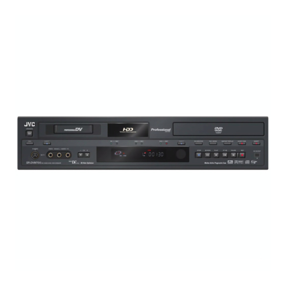
SR-DVM700EU
DVD
STANDBY/ON
DVD
TV
PR/CH
INPUT SELECT
PROG
NAVIGATION
RETURN
NEXT
SLOW
PAUSE
STANDBY/ON
ANGLE/
EE CHECK
DISPLAY
EJECT
DV
SET UP
S-VIDEO
INPUT
OUTPUT
VIDEO (MONO)L - AUDIO - R
SELECT
SELECT
IN F-1
TABLE OF CONTENTS
COPYRIGHT © 2006 Victor Company of Japan, Limited
REC
HDD
REC
DVD
REC
EJECT
DV/HDD/DVD
REC MODE
INSTANT REPLAY
STOP
REW
PLAY
FF
PAUSE
SR-DVM700EU [D5MC29]
Area Suffix
EU -------- Western Europe
AUDIO DUB.
INSERT
REC
DV IN/ OUT
No.YD091
2006/3
Advertisement

Related Manuals for JVC SR-DVM700EU


Summary of Contents for JVC SR-DVM700EU
-
Page 1: Table Of Contents
SELECT SELECT DV IN/ OUT IN F-1 SR-DVM700EU [D5MC29] Since the whole mechanism assembly unit is replaced, the DVD recorder mechanism of this unit need not be adjusted. TABLE OF CONTENTS PRECAUTION............... . . 1-3 SPECIFIC SERVICE INSTRUCTIONS . - Page 2 SPECIFICATION GENERAL Power requirement AC 220 V - 240 V~,50 Hz/60 Hz Power consumption Power on 42 W Power off Laser specification For CD Wavelength: 770 to 810 nm Output: 0.4 mW For DVD Wavelength: 653 to 663 nm Output: 1.0 mW Temperature Operating 5°C to 35°C...
-
Page 3: Precaution
SECTION 1 PRECAUTION SAFTY PRECAUTIONS Prior to shipment from the factory, JVC products are strictly in- Consequently, when servicing these products, replace the spected to conform with the recognized product safety and elec- cathode ray tubes and other parts with only the specified trical codes of the countries in which they are to be parts. - Page 4 1.1.2 Safety Check after Servicing Examine the area surrounding the repaired location for damage (4) Leakage current test or deterioration. Observe that screws, parts and wires have been Confirm specified or lower leakage current between earth returned to original positions, Afterwards, perform the following ground/power cord plug prongs and externally exposed ac- tests and confirm the specified values in order to verify compli- cessible parts (RF terminals, antenna terminals, video and...
- Page 5 Hard Disk Drive (HDD) Handling Precautions The HDD is a precision device for use in reading and writing a large amount of data on or from a disk rotating at a high speed. If it is not handled carefully, either abnormal operation may result or it may not be possible to read data. The HDD is sensitive to the following items and special care is required in safeguarding against them when handling an HDD.
-
Page 6: Specific Service Instructions
SECTION 2 SPECIFIC SERVICE INSTRUCTIONS Service position This unit has been designed so that the Mechanism and Main board assemblies can be removed together from the bottom chassis. Before diagnosing or servicing the circuit boards, take MAIN board assembly out the major parts from the bottom chassis. 2.1.1 How to set the "Service position"... - Page 7 Jig RCU mode This unit uses the following two modes for receiving remote con- 2.2.1 Changing Remote Control Code trol codes. (1) Slide the TV/DVD switch to DVD. (1) User RCU mode:Ordinary mode for use by the user. (2) Press the number key "1" of the remote control unit while (2) Jig RCU mode: Mode for use in production and servicing.
-
Page 8: Disassembly
SECTION 3 DISASSEMBLY Removing the major parts 3.1.1 Destination of connectors 3.1.2 How to read the procedure table This table shows the steps for disassembly of the externally fur- Two kinds of double-arrows in connection tables respectively nished parts and board assemblies. Reverse these steps when show kinds of connector/wires. - Page 9 < Note 2a > < Note 3a > • Be careful not to damage the connector and wire etc. during • When reattaching the bracket(DV MAIN), secure the screws connection and disconnection. (S13a) in the order of 1,2,3. • When connecting the flat wire to the connector, be careful with <...
- Page 10 (S1a) (S1a) (S1a) [1]Top cover (S1a) (S1a) (S1a) (S1a) (S1a) [10]Rear cover (S10b) (S9a) (S10b) (L10a) (S10a) [9]D-SUB board assembly (S12a) [11]DV mechanism assembly (L10a) (S11a) (S11a) (L10a) [12]Bracket (WR11b) <Note 2a> (S11a) (S12b) (S13a) (S12a) (WR11a) (S3b) (S3b) <Note 2a> (S3b) (S12b) [12]DV main board assembly...
- Page 11 DVD Drive unit section 3.2.1 Remove the top cover and tray (See figure 1, figure2, figure3, figure4) (1) The part a on the reverse side of a DVD drive unit is made Top cover to slide in the direction of an arrow. (A tray ejects a few.) Hook b (2) Remove the four screws A attaching the top cover.
- Page 12 3.2.2 Reassembly the tray (See figure 5) Shaft guide (1) The slide cam is done in the slide in the direction of the ar- row. (2) The shaft guide is done in the slide in the direction in the back. (3) The left side of the tray is inserted in the rail of the loading base, and the shaft guide is built in.
- Page 13 3.2.4 Remove the servo control board (See figure 7) (1) Disconnect the FFC wire from connector CN102, CN103, CN104, CN105 on the servo control board. (2) Remove the two screws D attaching the servo control board. (3) Hooks d is removed, and the servo control board is re- moved.
-
Page 14: Adjustment
SECTION 4 ADJUSTMENT Before adjustment (5) : Parts to be removed in disassembly/assembly, such as screws, washers and springs, and the points. 4.1.1 Precautions (1) Observe the specified screw tightening torque when Symbol Name & Point attaching parts. The torque should be 0.04 Nm (0.4 kgfcm) Screw unless otherwise specified. - Page 15 Disassembly/assembly of the mechanism assembly 4.2.1 Introduction The disassembly and assembly of the mechanism assembly should usually be performed in the ASSEMBLY mode.(Table 4-2-1) Note that the mechanism is in the cassette in (C-IN) mode when the mechanism assembly is taken out of the set and that the C-IN mode should be switched to the ASSEMBLY mode in this case.
- Page 16 2. Setting/checking the ASSEMBLY mode DC 3 V Motor bracket assembly (Loading Motor) Wire (Brown) Marking Wire (Red) (Colored red) Rotary encoder < ASSEMBLY > [ C ] [ H ] Fig.4-2-7 1-16 (No.YD091)
- Page 17 Mechanism timing chart See following table (Table 4-3-1). MODE ASSEMBLY LOADING END C-IN S. FF PLAY STOP FF/REW PARTS ROTARY ENCODER ROTARY ENCODER 33.33 166.66 193.33 226.66 273.33 306.66 MAIN CAM SUB CAM POLE BASE S/REV PLAY CTL PLATE FF/REW ON 1 MAIN BRAKE(SUP) ON 2...
- Page 18 Mechanism assembly/disassembly procedure table Step/Loc Point Note Discription Part Name Fig. No. [A] Cassette housing assembly/ [B] Mechanism assembly T 4-5-1 2(S1),(L1) (L5) [1] Drum assembly 4-5-2 3(S2) [2] Motor bracket assembly 4-5-2 4(S2) [3] Middle catcher assembly 4-5-3 3(S2) [4] Reel cover assembly 4-5-3 (S2), 2(L6)
- Page 19 TOP VIEW [ 2 ] [ 18 ] [ 19 ] [ 42 ] [ 1 ] [ 41 ] [ 3 ] [ 21 ] [ 9 ] [ 11 ] [ 23 ] [ 22 ] [ 25 ] [ 8 ] [ 5 ] [ 34 ]...
- Page 20 Disassembly/assembly 1. [A] Cassette housing assembly/ [B] Mechanism assembly Note 1a: If the wires for the cassette housing motor are connect- ( S1 ) ed to the circuit board, remove them before disassem- bly. ( S1 ) ( L2 ) ( L4 ) ( L5 ) <Note1a>...
- Page 21 3. [3] Middle catcher assembly/ [4] Reel cover assembly Note 3a: Once the reel cover assembly has been removed, the parts located below it tend to slip out easily: Be careful. ( S2 ) Note 3b: <Note3b> ( S2 ) [ 4 ] ( S2 ) ( S2 )
- Page 22 5. [9] Exit guide arm assembly/ [10] Swing arm assembly Note 5a: Exit guide arm assembly phase alignment. [ 9 ] <Note5a> Exit guide arm assembly [ 10 ] ( W1 ) This protrusion is combined to the dent of Charge arm assembly.
- Page 23 7. [14] Reel disk assembly (Supply) / [15] Reel disk assembly (Take up) / [16] Prism / [17] Control plate [ 14 ] [ 15 ] ( S2 ) [ 17 ] [ 16 ] ( L12 ) ( L12 ) [ 11 ] Fig.4-5-7 8.
- Page 24 9. [21] Ent. guide base assembly / [22] Worm wheel 2 / [23] Timing belt / [24] Center gear assembly Note 9a: How to attach the worm wheel 2 [22] . ( S2 ) [ 23 ] [ 22 ] [ 21 ] Phase alignment [ 34 ]...
- Page 25 11. [29] Tension control arm assembly/ [30] Brake control arm assembly / [31] Charge arm assembly Note 11a: ( L16 ) How to attach the tension control arm assembly [29] / Brake control arm assembly [30] . ( W1 ) [ 30 ] [34] ( L17 )
- Page 26 13. [34] Rotary encoder assembly / [35] Main cam / [36] Arm gear 1 assembly / [37] Centering arm assembly Note 13a: How to attach the rotary encoder assembly [34]. Mark (colored : red) [ 34 ] ( S2 ) ( S2 ) [ 35 ] <Note13a>...
- Page 27 14. [38] Sub cam / [39] Arm gear 2 assembly / [40] Clutch lock lever assembly Note 14a: How to attach the sub cam [38]. ( S2 ) Boss [ 39 ] <Note14a> [ 38 ] [ 38 ] <Note14a> Phase alignment Phase alignment [ 40 ]...
- Page 28 List of procedures or disassembly 14(S3) [ 14 ] (W2) (S2) (S2) [ 4 ] [ 7 ] [ 15 ] [ 10 ] (S2) [ 16 ] (S2) (P3) [ 8 ] (W1) [ 6 ] 6(S2) 9(S2) (S2) [ 12 ] 7(S2) 8(S2)
- Page 29 Mechanism phase check/adjustment See Fig 4-7-1. [ 36 ] [ 22 ] Worm wheel 2 Arm gear 1 assembly See Fig. 4-5-9a. See Fig. 4-5-13b. [ 34 ] Rotary encoder assembly See Figs. 4-5-9a and 4-5-13a. [ 39 ] Arm gear 2 assembly See Fig.
- Page 30 Mechanism disassembly/assembly sheet [ A ] [ 1 ] [ 2 ] [ 3 ] [ 4 ] [ 7 ] [ 11 ] Fig. No. Type Attachin 4-5-1 4-5-2 4-5-3 4-5-4 4-5-6 Ref. Fig. [A] Cassette housing assembly [1] Drum assembly [4] Reel cover assembly ( S2 ) ( S1 )
- Page 31 [ 16 ] [ 18 ] [ 19 ] [ 20 ] [ 21 ] [ 32 ] [ 33 ] [ 34 ] [ 38 ] [ 42 ] 4-5-7 4-5-8 4-5-9 4-5-12 4-5-13 4-5-14 4-5-15 [7] Band arm plate sub [ 11 ] Sub deck assembly [ 12 ] Main [ 13 ] Main...
- Page 32 Positioning the tension pole See Fig.4-9-1. [ B ] section [ C ] Tension arm sub assembly [ D ] section screw [A] Fig.4-9-1 4.9.1 Adjustment Method Note: • Remove the cassette housing assembly in advance. (1) Set the mechanism mode to the PLAY mode. (See 4.2.2 Mechanism modes) (2) Loosen a screw [A].
- Page 33 4.10 Compatibility and error rate adjustment 4.10.1 Preparation 4.10.2.2 Procedure Before disassembly and adjustment, back up the data stored in (1) Take out the 8 screws, then remove the top cover. (See the EEPROM (IC1504 on the DV MAIN board) using the Service SECTION 3 DISASSEMBLY) Support System Software (SSS software).
- Page 34 4.10.3 Linearity adjustment 4.10.4 PB switching point adjustment The following flowchart shows the linearity check/adjustment The following flowchart shows the PB switching point adjustment procedure. procedure. Connect an oscilloscope (CH: + Slope) and, while Load the alignment tape. triggering it with the HID signal, observe the ENV OUT The “PB Switching Point”...
- Page 35 4.11 Electrical adjustment (DV SECTION) 4.11.1 Precautions 4.11.4 Setup (1) The DV section of this model is based on a special adjust- 1. Setup for computer adjustment ment method using a PC. However, ordinary adjustment is - Setup by extending the jig connector - required only when the part listed below has been re- placed.
- Page 36 4.12 Electrical adjustment (DVD SECTION) Note: 4.12.1.2 EE Y level The following adjustment procedures are not only necessary Signal (A1) • Ext. input after replacement of consumable mechanical parts or board (A2) • Color (colour) bar signal assemblies, but are also provided as references to be referred Mode •...
- Page 37 4.12.1.5 EE COMPONENT PB/CB level Signal • Internal colour bar Mode • EE Equipment • Oscilloscope Specified Measuring point (D) • COMPONENT PB/CB terminal value (G) EVR mode (F1) • Jig code “43-95” EVR address (F2) • "ADJUST06 : **" Fig.4-12-3 EE composite burst level (F3) •...
-
Page 38: Troubleshooting
SECTION 5 TROUBLESHOOTING Manually removing the cassette tape If a loaded cassette tape cannot be ejected due to a failure in the (3) If the tape is slack, wind it up by turning the shaft on the top- electrical circuitry, take the cassette tape out using the following side of the capstan motor in the direction of the arrow using procedure. - Page 39 Manually removing the disk(DVD/CD) If you cannot remove the disk which is loaded because of any electrical or mechanical failures, manually remove it by taking the fol- lowing steps. 5.2.1 Method 1 (1) AC Plug is pulled out at once and inserted again. (2) It is displayed on FDP as "PLEASE"...
- Page 40 GG: Type of the DV cassette tape (4) Transmit the code "43-59" from the Jig RCU once again. : Key code (JVC code) The FDP shows the EMG detail information < 3 > in the : EMG content display < 1 >...
- Page 41 5.3.5 EMG detail information < 1 > 5.3.6 EMG detail information < 2 > The status (electrical operation mode) of the unit and the status FF : DV mechanism sensor information (mechanism operation mode/mechanism position) of the mech- Display DV mechanism sensor information Display DV mechanism sensor information anism in the latest EMG can be confirmed based on the figure in...
- Page 42 Display function of DVD section 5.4.1 Displaying SYSTEM INFO SYSTEM INFO contains information on firmware version of the unit and the mechanism drive, and an initialize execution menu. (1) Set the unit to the Jig RCU mode. (2) Press DV/HDD/DVD SELECT button on the unit repeatedly so that the HDD lamp lights up on the unit. (3) Transmit "43-8b"...
- Page 43 5.4.3 Updating the firmware of the unit • Firmware update disc supports CD-R media. • When firmware update is necessary, information is available from the website of DIGITAL VIDEO STORAGE CATEGORY, CS group. 5.4.3.1 Creating an update disc Please check the details of the update disc creation method by JS-NET. (1) Down load the update file from JS-NET.
- Page 44 5.4.5 Initialization to the factory shipment state When the initialization is operated, internal information changes as follows. It is essential to obtain the client’s permission before the operation. • All DVD library is all deleted. • All the DVD initial settings go back to the initial status. (1) Set to the Jig RCU mode.
- Page 45 (No.YD091)1-45...
- Page 46 Victor Company of Japan, Limited DIGITAL VIDEO STORAGE CATEGORY 12, 3-chome, Moriya-cho, kanagawa-ku, Yokohama, kanagawa-prefecture, 221-8528, Japan (No.YD091) Printed in Japan...
- Page 47 STOP PLAY PAUSE SELECT SELECT DV IN/ OUT IN F-1 SR-DVM700EU [D5MC29] Since the whole mechanism assembly unit is replaced, the DVD recorder mechanism of this unit need not be adjusted. No.YD091SCH COPYRIGHT 2006 Victor Company of Japan, Limited 2006/3...
- Page 49 CIRCUIT BOARD NOTES CHARTS AND DIAGRAMS 1. Foil and Component sides NOTES OF SCHEMATIC DIAGRAM 4. Voltage measurement 1) Foil side (B side) : Parts on the foil side seen from foil face (pattern face) 1) Regulator (DC/DC CONV) circuits Safety precautions are indicated.
- Page 50 Wiring diagram C N 5 0 0 1 Q G A 7 9 0 1 C 3 - 0 2 E U : A C 2 2 0 V - 2 4 0 V L I V E 5 0 H z C N 5 3 0 5 N E U T R A L U S :...
- Page 51 Standard schematic diagrams Switching regulator section S W . R E G M A I N ( R E G ) L 5 2 0 3 1 0 u D 5 3 0 5 U F 2 0 2 G - F 2 6 Q 5 3 1 3 H E R 2 0 2 G - B 3 2 2 - 3 2 S A 1 5 8 5 S / Q R /...
- Page 52 Video interface section TO CN5502 SHEET 1 CN1003 VDDI1.8 DIGI3.3V IC1002 D2.5V TO SHEET 4 D1.8V C1042 K_BUS_OUT K_BUS_IN TO SHEET 7 RA1003 RA1005 P_CTL[H] R1036 SYS_RESET[L] AI_D[0] R1035 C1043 C1047 TO SHEET 4 K_BUS_REQ Q1002 C1088 A_MUTE2[H] K_BUS_CLK R1037 CN1002 C1044 C1046...
- Page 53 Flash-ROM section C1207 IC1203 IC1201 K1201 C1203 R1216 C1204 B1203 R1222 B1202 R1223 R1224 C1206 B1204 IC1202 R1225 R1226 TL1215 TL1216 CN1202 D3.3V B1205 MADD[22] R1227 UART2_RX R1228 UART2_TX B1206 TO SHEET 4 CS[0] CS[1] E5_RESET[L] MADD[1-5] MADD[6-21] RA1201 R1217 R1218 R1219 RA1202...
- Page 54 Media processor section AO_D[0] SDRAM_A[14-17] AO_SCLK SDRAM_VREF AO_FSYNC SDRAM_CLK_L[1] AO_IEC958 SDRAM_CLK[1] SHEET 2 AO_MCLKO SDRAM_CLK_L[0] AI_D[0] SDRAM_CLK[0] VIDEO_MUTE[H] SDRAM_WE_L TO SHEET 5 PHY_CNA SDRAM_CKE 480I[H] SDRAM_RAS_L SHEET 6 SDRAM_CAS_L SDRAM_DQM[0-3] SDRAM_DQS[0-3] SDRAM_A[0-13] SDRAM_DQ[16-31] B1404 SDRAM_DQ[0-15] SHEET 2 R1471 B1405 R1470 R1472 R1469 C1459...
- Page 55 DDR-SDRAM Section IC1603 IC1603 IC1603 IC1603 IC1604 IC1604 IC1604 IC1604 DIGITAL(DDR_SDRAM) RA1621 RA1617 RA1609 C1626 C1634 C1621 C1629 RA1622 RA1610 RA1618 C1625 C1633 RA1623 RA1611 RA1619 C1622 C1630 C1624 C1632 RA1624 RA1612 RA1620 C1623 C1631 C1649 R1619 C1651 C1643 R1625 C1659 C1661 RA1613...
- Page 56 IEEE1394 section B1802 B1801 C1806 L1802 L1801 C1804 C1803 C1814 C1813 C1805 R1820 T1804 T1804 T1804 T1804 CN1802 C1810 K1801 X1801 TO CN7121 SHEET 23 D3.3V T1803 T1803 T1803 T1803 PHY_RESET[L] PHY_LREQ R1801 PHY_CLK R1802 PHY_CNA TO SHEET 4 PHY_CTL[0] PHY_CTL[1] PHY_DATA[0-7] PHY_LPS...
- Page 57 ATAPI Interface section CN2101 R2104 ATA2_RESET ATA2_DAT[0-15] K2101 ATA2_DMARQ RA2101 K2102 ATA2_DIOW[L] K2103 ATA2_DIOR[L] K2104 ATA2_IORDY TO SHEET 4 K2105 ATA2_DMAACK[L] RA2102 K2106 ATA2_INTRQ K2107 ATA2_ADD[0-4] K2108 D5.0V K2109 D3.3V RA2103 K2110 K2111 RA2201 K2112 K2113 R2101 R2102 R2103 RA2104 K2114 K2115 RA2202...
- Page 58 On screen section R210 R211 C205 C201 C208 R201 C203 B201 TO SHEET 11 V_FROM_OSD Q202 R207 L202 R204 C204 R206 L201 Q201 R205 C202 B206 B204 R202 C207 R208 R209 B202 V_FROM_OSD B205 B203 TO SHEET 9 CHARA_DATA R203 V_TO_OSD TO SHEET 9, 10 C209...
- Page 59 DV video switch section L502 R533 Q513 R531 C561 CN501 R532 TO CN3501 R542 R510 C549 C536 C535 C562 C527 SHEET 20 Q505 C551 C547 DV_Y_OUT L504 DV_C_OUT SHEET 10 C548 R521 L503 R513 L501 C557 TO SHEET 8 C550 C552 R518 R519...
- Page 60 Video switch section SW5V SHEET 1 L706 R711 I2C_DATA_A/V R712 I2C_CLK_A/V R746 TO SHEET 13 R742 Q706 R748 C771 B702 L702 X701 C772 Q705 C769 R744 R745 L707 C767 R743 C768 R747 R733 R710 R717 C736 C735 Q713 R731 C749 C727 Q701 C747...
- Page 61 Terminal section REAR_Y_IN REAR_C_IN J901 REAR_V_IN R942 C_OUT_BIAS R941 DV_Y_OUT TO SHEET 9 C929 DV_C_OUT TO_DV_DUB_C TO_DV_DUB_Y TU_VIDEO R943 R961 C981 R962 C982 L902 R911 R912 R910 REAR_Y_IN C903 C904 REAR_C_IN Q904 TO SHEET 10 REAR_V_IN R907 VDR_C_OUT_BIAS Q905 C918 R922 TU_VIDEO B911...
- Page 62 Audio input/output section TO CN3701 CN2601 R2201 SHEET 21 C2201 R2204 IC2201 IC2202 C2202 R2208 R2210 R2209 Q2201 A.IN1[R] Q2203 R2207 R2206 TO SHEET 11 A.IN1[L] R2205 Q2204 Q2202 R2202 R2203 TO CN8001 SHEET 24 CN2602 R2612 R2615 DEMOD[R] NOT USED DEMOD[L] IC2603 IC2604...
- Page 63 System controller section I2C_DATA_A/V I2C_CLK_A/V FRONT_Y_IN SHEET 10 FRONT_C_IN WIDE_DET_VDR CN3104 TO CN7201 SHEET 15 I2C_DATA2 I2C_CLK2 TO SHEET 9 WIDE_DET_DV P.MUTE_DV[L] F.AUDIO[L] FRONT_C_IN F.AUDIO[R] FRONT_Y_IN DVD_A_INSEL1 C3032 TO SHEET 10 FRONT_V_IN R3275 R3276 DVD_A_INSEL2 C3034 C3035 DVC_A_INSEL1 R3081 DVC_A_INSEL2 SHEET 12 R3080 C3038...
- Page 64 DC/DC Converter section R5730 R5721 R5731 C5727 IC5701 C5731 R5732 R5711 C5730 R5720 C5720 C5710 D5720 R5710 D5710 C5712 C5722 C5721 C5711 C5732 Q5720 R5713 C5716 C5726 R5723 R5712 IC5710 C5723 R5722 K5720 L5720 L5710 K5710 C5713 D5721 C5725 C5724 C5714 C5715 CN5701...
- Page 65 Switch jack. Switch display and Jack section C7201 D7202 D7203 R7202 J7201 S7213 L7202 J7201 R7213 C7203 C7202 S7034 S7033 S7032 S7025 S7035 S7023 S7212 L7203 L7201 J7201 R7212 C7205 C7204 S7014 S7013 S7024 S7012 S7015 S7004 S7211 R7211 J7204 D7204 R7207 R7206...
- Page 66 DV Regulator section ZP101-10 ZP101-11 ZP101-12 SW_3V ZP101-3 CN1001 A_REG_3V ZP101-2 B1005 L1001 B1001 ZP101-1 D_REG_3V B1002 SW_5V[-] LC1002 L1002 SW_5V TO EACH SHEET LC1003 Q1005 B1003 B1004 L1003 TO CN5404 ZP101-4 A_REG_5V SHEET 1 LC1004 L1004 R1011 R1009 Q1007 C1002 Q1001 IC1005...
- Page 67 DV MSD Section SW_3V L1501 TO SHEET 16 REG_5V CN1502 ZP152-1 ZP152-2 ZP152-3 ZP152-4 R1613 DRWSEL Q1511 Q1513 ZP152-5 ZP152-6 DALE ZP152-7 ADDT00 TO DV ZP152-8 ADDT01 ZP152-9 ADDT02 ZP152-10 ADDT03 ZP152-11 ADDT04 R1611 Q1512 ZP152-12 ADDT05 ZP152-13 ADDT06 ZP152-14 ADDT07 ZP152-15 ADDT08...
- Page 68 DV Main section ADDT15 ADDT14 ADDT13 ADDT12 ADDT11 ADDT10 C2086 ADDT09 ADDT08 R2131 ADDT07 IC2001 ADDT06 TO SHEET 17 ADDT05 ADDT04 ADDT03 ADDT02 ADDT01 ADDT00 R2132 DV_WAIT C2036 DRWSEL C2037 DALE HID1 JLIP_RX JLIP_TX OUTV TO SHEET 17 DAC_DATA OUTH DAC_CLK DCO3 RESET...
- Page 69 DV input/output section Y_GCTL C_GCTL DV_Y SHEET 20 DV_C AGC_GAIN Y/V_IN DUMP_CTL C_IN ATF_GAIN SHEET 22 RECCADJ IC3151 L3151 L3022 C3132 C3012 C3131 C3011 L3021 R3102 R3105 C3101 C3022 C3021 R3079 C3014 Q3101 Q3102 R3103 R3008 EXT_IN_L R3106 DAC_DATA DAC_CLK C3001 DAC_CS R3003...
- Page 70 DV Video output section L3521 A_REG_5V REG_3V TO SHEET 16 C3521 L3522 C3523 R3556 R3557 C3515 R3555 C3513 R3514 C3552 C3508 R3558 Q3522 C3537 B3502 IC3501 R3529 R3527 Q3503 L3533 L3534 R3526 C3540 C3536 C3538 C3539 R3528 R3552 R3553 C3532 R3551 C3551 R3524...
- Page 71 Audio AD/DA section L3702 SW_5V L3701 A_REG_3V TO SHEET 16 SW_5V[-] C3731 C3730 C3733 C3734 R3725 R3719 C3717 R3726 R3713 R3712 R3714 C3735 C3737 C3736 R3721 R3720 CN3701 R3727 R3711 ZP371-1 R3710 ZP371-2 R3709 C3718 AIBCK ZP371-3 R3708 AIMCK ZP371-4 R3707 TO CN2601 AILRCK...
- Page 72 DV PRE/REC section L4005 C4015 C4013 C4026 C4027 R4009 HID3 PB_H SHEET 17 REC_H HID1 R4008 R4010 C4014 L4011 R4022 R4038 C4054 C4051 C4030 C4029 C4028 Q4001 C4052 R4036 R4033 R4039 R4024 R4031 R4040 C4053 R4023 Q4003 C4062 C4061 Q4002 Q4004 C4065 R4025...
- Page 73 Junction (Video) section TO SHEET 24 TO SHEET 24 TO CN1001 SHEET 2 TO CN701 TO CN1002 SHEET 2 SHEET 10 C7143 C7142 C7141 K7104 K7103 K7102 R7153 R7152 CN7102 TO CN3103 C7137 SHEET 13 B7121 B7122 B7123 B7115 B7124 B7113 B7125 B7131...
- Page 74 Junction (audio) section ADC_RST[L] TO SHEET 23 A.MUTE_VDR[H] K8201 Q8005 R8233 C8232 C8231 CN8001 Q8003 Q8004 R8222 R8221 R8220 R8219 C8210 C8209 TO CN2602 R8210 SHEET 12 R8209 C8206 R8212 C8207 C8208 Q8002 R8208 C8205 R8211 R8207 C8052 C8053 R8232 K8202 R8231 R8202...
- Page 75 RS232C Terminal section IC7401 CN7401 J7401 TO CN1405 C7405 SHEET 4 C7401 C7402 C7403 C7404 p40054001a_rev0 SHEET 25 2-53 2-54...
- Page 76 Printed circuit boards Junction board <92> LPB10314-001B Switching regulator board <01> LPB10314-001B DANGEROUS VOLTAGE CN8001 Q8002 CN7102 R8208 C8207 R8207 C8205 IC8201 R5106 C5006 D5106 R8231 IC8202 R8201 C8202 C8201 C8203 C5105 C8056 IC5101 C5104 C8204 C8055 D5104 R5107 C8057 R5108 D5105 Q8003...
- Page 77 Main board <03> LPB10277-001D CN3002 CN3103 CN3014 CN2602 CN5402 K7302 C7301 K7304 C7304 CN7301 CN3901 K7301 D3010 CP5402 K7303 C7303 C7302 R3041 C905 R934 Q909 CN901 C921 R936 R918 B916 C920 Q908 B3002 Q703 CN701 R935 B915 R932 R933 R3204 R717 R510 C527...
- Page 78 COMPONENT PARTS LOCATION GUIDE <MAIN> LPB10277-001D FDP Grid assignment and anode connection REF.NO. LOCATION REF.NO. LOCATION REF.NO. LOCATION REF.NO. LOCATION REF.NO. LOCATION REF.NO. LOCATION REF.NO. LOCATION CAPACITOR C735 B C 15L C5404 B C 13E L701 A D 17M R510 B C 8N R963 B C 19E...
- Page 79 Jack, Operation/Jack, Display/Switch and D-Sub board DC/DC Converter board <11> LPB20041-002B Forward side Reverse side CN5702 <27>OPERATION/JACK R5732 CN5702 R5730 IC5701 LPB10314-001B R5731 COMPONENT PARTS LOCATION GUIDE <OPERATION/JACK> LPB10314-001B C5731 REF.NO. LOCATION REF.NO. LOCATION REF.NO. LOCATION REF.NO. LOCATION C5732 CAPACITOR CONNECTOR RESISTOR OTHER...
- Page 80 Digital board <02> LPB10256-001B Reverse side Forward side ZP15 ZP17 ZP19 ZP22 ZP86 ZP212 ZP84 ZP210 ZP78 ZP74 ZP70 ZP209 ZP67 ZP65 ZP63 ZP61 ZP59 ZP57 ZP55 ZP53 ZP51 ZP49 ZP88 ZP211 ZP82 ZP80 ZP76 ZP72 CN2201 ZP32 ZP36 ZP40 D2201 ZP68 ZP66...
- Page 81 DV Main board <50> LPB10270-001C Reverse side Forward side ZP200-3 ZP200-6 ZP200-5 ZP200-2 ZP200-1 ZP200-4 CN2002 R3116 R3115 R3136 R3135 ZP351-4 ZP351-6 L3112 C2020 L3521 R2031 D2002 R3545 L3522 C3120 R3003 R2027 R3556 C3012 ZP351-7 Q3112 R2041 R2046 ZP351-5 R3004 C2015 C3540 C3124...
- Page 82 Block diagrams Digital section DIGITAL VIDEO IF DDR SDRAM IC1601 RA1609 SDRAM_DQ[0-15] DDR_DQ[0-15] SW. REG D2.5V, D1.8V, D3.3V IC1603 CN5502 DDR SDRAM RA1612 SW5V, D5V, V3.3V JUNCTION IC1602 RA1613 (VIDEO) AO_IEC958, AI_D[0], A_MUTE2[H], K_BUS_CLK SDRAM_DQ[16-31] DDR_DQ[16-31] K_BUS_REQ, SYS_RESET[L], K_BUS_IN/OUT IC1604 CN7109 DDR SDRAM RA1616...
- Page 83 VIDEO (1) Section TO_DV_DUB_Y TO_DV_DUB_C JUNCTION (VIDEO) V_FROM_OSD REAR_Y_IN REAR_C_IN REAR_V_IN CN7123 CN701 DV_Y_OUT YTODIGI DV_C_OUT TO DIGITAL CTODIGI (VIDEO IF) FRONT_C_IN CN7108 CN1001 FRONT_Y_IN IC7101 FRONT_V_IN VYIN MAIN (TERMINAL, VDR V SW) COUT 75 DRV YVOUT FILTER -6dB CBOUT SYSCON USED 75 DRV...
- Page 84 VIDEO (2) Section TO_DV_DUB_Y TO_DV_DUB_C MAIN (VIDEO SW VDR) V_FROM_OSD REAR_Y_IN REAR_C_IN REAR_V_IN DV_Y_OUT DV_C_OUT FRONT_C_IN FRONT_Y_IN FRONT_V_IN SYSCON I2C_DATA2 I2C_CLK2 CN501 D_C_IN D_Y/V_IN DV ( VIDEO OUT ) D_Y_OUT CN3501 D_C_OUT USED WF15 USED USED EE/PB SP/EP WF16 DATA S-VHS LOGIC Pre LPF2...
- Page 85 AUDIO Section MAIN (AUDIO I/O, TERMINAL I/O, TUNER) SW/JACK CN7201 CN3104 J7201 F.AUDIO[L] F.AUDIO[L] AUDIO IN(L) DVC_A_INSEL1 DVC_A_INSEL2 F.AUDIO[R] F.AUDIO[R] DVD_A_INSEL1 AUDIO IN(R) DVD_A_INSEL2 SYSCON A.OUTSEL1 A.OUTSEL2 A.MUTE_DVC(H) IC2201 IC2202 CN2601 DV_A_REC[L] DV_A_REC[R] JUNCTION (AUDIO AD/DA, VIDEO) 9,10 IC2603 TO DV MAIN DVC_A_INSEL1 DVC_A_INSEL2 (AUDIO AD/DA)
- Page 86 System control section MAIN ( SYSCON, ON SCREEN ) DV MAIN (MSD) LOADING MOTOR IC1501 IC3001 LOAD.MOTOR+ LOAD.MOTOR- (DV MSD) DAC_DATA ( SYSTEM CONTROL MICRO PROCESSOR ) DAC_CLK DAC_CS DAC_CS TBC_IN TBC_SDI OSC2(OUT) CN1501 TBC_CLK X3002 TBC_CLK MDA_CS MAIN SYSTEM MDA_CS TBC_CS TBC_CS...
- Page 87 VIDEO (DV) Section DV MAIN (DV MAIN, DV I/O, DV VVIDEO OUT, AUDIO AD/DA, DV PRE/REC) IC3151 DAC_CS AD CONV. DAC_CLK DAC_DATA TBC_CLK TBC_SDI DV MSD DUMP_CTL TBC_CS AGC_GAIN TBC_RST ATF_GAIN TBC_SDO RECCADJ TBC_VD M_VCOCTL CLK27A FSPLLCTL IC3501 Y_GCTL VIDEO AMP Y_GCTL C_GCTL D-SUB...
- Page 88 CPU PIN FUNCTION WAVEFORMS <SYSCON IC3001> PIN NO. LABEL IN/OUT FUNCTION PIN NO. LABEL IN/OUT FUNCTION VIDEO BLOCK DIAGRAM(1) TO_VSS DV_H_SW DETECTION OF DVC CASSETTE SVss CONNECTED Vcc IC701-5 IC701-7 IC701-9 IC701-11 IC701-14 IC701-45 IC701-47 OPEN NOT CONNECTED JUST/EDS[H] VIDEO SIGNAL FIELD DETECT TO_VSS TU_CLK SERIAL DATA TRANSFERMER CLOCK TO TUNER...
- Page 89 VOLTAGE CHARTS <SW.REG> <MAIN> <SWITCH/DISPLAY> <DV MAIN> MODE MODE MODE MODE MODE MODE MODE MODE MODE MODE MODE MODE MODE MODE MODE PLAY PLAY PLAY PLAY PLAY PLAY PLAY PLAY PLAY PLAY PLAY PLAY PLAY PLAY PLAY PIN NO. PIN NO. PIN NO.
- Page 90 VOLTAGE CHARTS <JUNCTION> <D-SUB> MODE MODE MODE MODE MODE PLAY PLAY PLAY PLAY PLAY PIN NO. PIN NO. PIN NO. PIN NO. PIN NO. IC5501 IC7401 CN7102 IC5502 Q5504 -16.8 -16.8 -16.7 -16.6 -16.1 -16.0 CN7123 Q5505 -8.6 -8.5 Q5508 CN7126 CN7401 IC5503...
- Page 92 Victor Company of Japan, Limited Digital Video Storage Category 12, 3-chome, Moriya-cho, kanagawa-ku, Yokohama, kanagawa-prefecture, 221-8528, Japan Printed in Japan No.YD091SCH...
- Page 93 * BEWARE OF BOGUS PARTS Parts that do not meet specifications may cause trouble in regard to safety and performance. We recommend that genuine JVC parts be used. * (x_) in a description column shows the number of the used part.
- Page 94 Exploded view of general assembly and parts list Block No.M1MM D-SUB BOARD ASSY<97> DV MECHANISM ASSY<M2> DV MAIN BOARD ASSY<50> SWITCHING REGULATOR BOARD ASSY<01> MAIN BOARD ASSY<03> DV JACK BOARD ASSY<36> DIGITAL BOARD ASSY<02> JUNCTION BOARD ASSY<92> 3-2(No.YD091)
- Page 95 D-SUB BOARD ASSY D-SUB CN852 CN7401 SWITCHING REGULATOR CN5001 CN5302 BOARD ASSY MAIN BOARD ASSY WR20 WR10 WR15 WR13 WR17 WR16 WR11 CN5303 CN5304 CN5403 CN7107 CN5501 CN5404 CN701 WR14 CN7123 CN3501 CN1001 CN3701 CN1505 DV MAIN BOARD ASSY CN1003 CN1501 CN2101 C545...
- Page 96 General assembly Block No. [M][1][M][M] Symbol No. Part No. Part Name Description Local 1 LP10574-008A FRONT PANEL ASSY LP30756-005A C.DOOR(DV) LP40688-001A SPRING(DV) QYTDSF2608ZA TAP SCREW M2.6 x 8mm DISPLAY/SWITCH(x5) QYTDSF2608ZA TAP SCREW M2.6 x 8mm OPERATION/JACK(x5) 4 LP10460-022A TOP COVER (SERVICE)
- Page 97 DVD mechanism assembly and parts list Block No.M2MM CLAMPER SA (No.YD091)3-5...
- Page 98 DVD mechanism Block No. [M][2][M][M] Symbol No. Part No. Part Name Description Local LP10590-002B LOWER CASE LP41183-001A MOTOR PULLEY QAR0347-001 LOADING MOTOR LP41117-001A SCREW (x2) LP41290-001A BELT LP31519-002A PULLEY GEAR LP31521-001A MIDDLE GEAR LP31523-001A MIDDLE GEAR 2 LP31520-001A DRIVE GEAR LP21396-001A SLIDE CAM LP21397-001A...
- Page 99 DV mechanism assembly and parts list Block No. M3MM Classifi- Symbol in Part No. cation drawing AA BB Grease KYODO-SH-P KYODO-SH-JB YTU94027 NOTE:The section marked in AA and BB indicate lubrication and greasing areas. (No.YD091)3-7...
- Page 100 DV mechanism Block No. [M][3][M][M] Symbol No. Part No. Part Name Description Local PRD10428A MAIN DECK ASSY LY30358-001B DRUM BASE DECK YQ43893 MINI SCREW (x3) LY30343-001A WORM WHEEL 2 LY40237-001C ENT.GUIDE BASE ASSY YQ43893 MINI SCREW LY30341-001B MOTOR BRACKET ASSY YQ43893 MINI SCREW (x4)
- Page 101 C5208 QEZ0700-128 E CAPACITOR 1200uF 10V M Q5304 or UN2211-X TRANSISTOR C5209 QEZ0658-186Z E CAPACITOR 18uF 50V M Q5305 2SC3576-JVC-T TRANSISTOR C5210 QEZ0653-227Z E CAPACITOR 220uF 6.3V M Q5305 or 2SD2144S/VW/-T TRANSISTOR C5211 QEZ0658-186Z E CAPACITOR 18uF 50V M Q5306...
- Page 102 Symbol No. Part No. Part Name Description Local Symbol No. Part No. Part Name Description Local F5001 QMF51W2-2R0-J8 FUSE 2A AC250V FC5001 QNG0020-001Z FUSE CLIP C1001 NBE20JM-226X TA E CAPACITOR 22uF 6.3V M FC5002 QNG0020-001Z FUSE CLIP C1002 NBE20JM-106X TA E CAPACITOR 10uF 6.3V M...
- Page 103 Symbol No. Part No. Part Name Description Local Symbol No. Part No. Part Name Description Local C1430 NCB31CK-104X C CAPACITOR 0.1uF 16V K C1706 NCB31CK-104X C CAPACITOR 0.1uF 16V K C1435 NBE20JM-106X TA E CAPACITOR 10uF 6.3V M C1707 NCB31CK-104X C CAPACITOR...
- Page 104 Symbol No. Part No. Part Name Description Local Symbol No. Part No. Part Name Description Local R1072 NRSA63J-0R0X MG RESISTOR 0Ω 1/16W J R1491 NRSA63J-102X MG RESISTOR 1kΩ 1/16W J R1217 NRSA63J-101X MG RESISTOR 100Ω 1/16W J R1493 NRSA63J-0R0X MG RESISTOR 0Ω...
- Page 105 Symbol No. Part No. Part Name Description Local Symbol No. Part No. Part Name Description Local R2107 NRSA63J-220X MG RESISTOR 22Ω 1/16W J RA2211 NRZ0040-330X NET RESISTOR 33Ω 1/16W J x4 R2108 NRSA63J-820X MG RESISTOR 82Ω 1/16W J R2109 NRSA63J-220X MG RESISTOR...
- Page 106 Symbol No. Part No. Part Name Description Local Symbol No. Part No. Part Name Description Local K2202 NQR0129-002X FERRITE BEADS Q711 or 2SA1037AK/QR/-X TRANSISTOR K2203 NQR0129-002X FERRITE BEADS Q711 or 2SA1530A/QR/-X TRANSISTOR K2204 NQR0129-002X FERRITE BEADS Q713 2SB709A/QR/-X TRANSISTOR K2205 NQR0129-002X...
- Page 107 Symbol No. Part No. Part Name Description Local Symbol No. Part No. Part Name Description Local D3004 10EDB20-T2 SI DIODE C710 NCB31EK-103X C CAPACITOR 0.01uF 25V K D3005 10EDB20-T2 SI DIODE C712 NCB31EK-103X C CAPACITOR 0.01uF 25V K D3007 1SS355-X DIODE C.M...
- Page 108 Symbol No. Part No. Part Name Description Local Symbol No. Part No. Part Name Description Local C2651 QEKJ1CM-476Z E CAPACITOR 47uF 16V M R744 NRSA63J-471X MG RESISTOR 470Ω 1/16W J C2653 QEKJ1CM-476Z E CAPACITOR 47uF 16V M R745 NRSA63J-821X MG RESISTOR 820Ω...
- Page 109 Symbol No. Part No. Part Name Description Local Symbol No. Part No. Part Name Description Local R2629 NRSA63J-472X MG RESISTOR 4.7kΩ 1/16W J R3207 NRSA63J-0R0X MG RESISTOR 0Ω 1/16W J R2630 NRSA63J-472X MG RESISTOR 4.7kΩ 1/16W J R3218 NRSA63J-0R0X MG RESISTOR 0Ω...
- Page 110 Symbol No. Part No. Part Name Description Local Symbol No. Part No. Part Name Description Local B5403 NRSA63J-0R0X MG RESISTOR 0Ω 1/16W J NRSA63J-0R0X MG RESISTOR 0Ω 1/16W J CN501 QGF1040C1-07 CONNECTOR FFC/FPC (1-7) NRSA63J-0R0X MG RESISTOR 0Ω 1/16W J CN701 QGF1207C1-04 CONNECTOR...
- Page 111 Operation/jack board Symbol No. Part No. Part Name Description Local Block No. [2][7] D7044 SLR-343VC-T DVD REC Symbol No. Part No. Part Name Description Local D7046 SLR-343MC-T D7047 SLR-343MC-T LPA10314-01B5 OPERATON JACK BOARD ASSY C7001 NCB31EK-104X C CAPACITOR 0.1uF 25V K C7002 QCFB1HZ-104Y...
- Page 112 DV main board Symbol No. Part No. Part Name Description Local Block No. [5][0] C1003 NEAF0JM-107X E CAPACITOR 100uF 6.3V M Symbol No. Part No. Part Name Description Local C1004 NCB31CK-104X C CAPACITOR 0.1uF 16V K C1005 NEAF0JM-107X E CAPACITOR 100uF 6.3V M C1006...
- Page 113 Symbol No. Part No. Part Name Description Local Symbol No. Part No. Part Name Description Local C2052 NCB10JK-106X C CAPACITOR 10uF 6.3V K C3513 NCB31CK-104X C CAPACITOR 0.1uF 16V K C2055 NEAF0JM-226X E CAPACITOR 22uF 6.3V M C3514 NCB31CK-104X C CAPACITOR 0.1uF 16V K...
- Page 114 Symbol No. Part No. Part Name Description Local Symbol No. Part No. Part Name Description Local R1002 NRSA63J-102X MG RESISTOR 1kΩ 1/16W J R2050 NRSA63J-222X MG RESISTOR 2.2kΩ 1/16W J R1003 NRSA63J-103X MG RESISTOR 10kΩ 1/16W J R2052 NRSA63J-0R0X MG RESISTOR 0Ω...
- Page 115 Symbol No. Part No. Part Name Description Local Symbol No. Part No. Part Name Description Local R3506 NRSA63J-680X MG RESISTOR 68Ω 1/16W J RA1510 NRZ0040-473X NET RESISTOR 47kΩ 1/16W J x4 R3515 NRSA63J-471X MG RESISTOR 470Ω 1/16W J R3516 NRSA63J-0R0X MG RESISTOR...
- Page 116 QETN1CM-106Z E CAPACITOR 10uF 16V M IC8202 or AK4385VT-X C8010 QETN1CM-106Z E CAPACITOR 10uF 16V M C8011 QETN1HM-475Z E CAPACITOR 4.7uF 50V M Q5504 2SC3576-JVC-T TRANSISTOR C8012 NCB31HK-104X C CAPACITOR 0.1uF 50V K Q5504 or 2SD2144S/VW/-T TRANSISTOR C8013 QETN0JM-107Z E CAPACITOR 100uF 6.3V M...
- Page 117 CN7109 QGB2027M4-20S CONNECTOR B-B (1-20) CN7121 QGB2027M9-14 CONNECTOR DV JACK2 CN7123 QGF1207C1-04 CONNECTOR VIDEO IN 2 CN7124 QGF1207C1-04 CONNECTOR JIG(JVC DR CN7126 QGA2001C1-06 CONNECTOR DV JACK CN7127 QGA2001C1-06 CONNECTOR DV JACK DV CN8001 QGB1231M1-11 CONNECTOR AUDIO CP5501 QMFZ053-2R0Z-J1 FUSE ...
- Page 118 Packing materials and accessories parts list Block No. M4MM ADHESIVE TAPE GENERAL ASSY<M1> SPEC OF BARCODE 3-26(No.YD091)
- Page 119 Packing and accessories Block No. [M][4][M][M] Symbol No. Part No. Part Name Description Local LP31469-014A PACKING CASE LP31454-002A CUSHION ASSY PQM30021-105 POLY BAG LP31561-002A SHEET ------------ BATTERY R6 TYPE(x2) QAM0498-001 A/V CABLE QPC02202230P POLY BAG CABLE 8 QAM0001-001 CONVERSION PLUG ...