Table of Contents
Advertisement
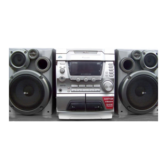
Quick Links
All manuals and user guides at all-guides.com
SERVICE MANUAL
Ver 1.0 2004.03
CX-JPK33 is the amplifier, CD player, tape deck
and tuner section in JAX-PK33.
Amplifier section
The following measured at AC 120, 127, 220, 240 V
50/60 Hz
DIN power output (rated): 48 + 48 watts (6 ohms at
1 kHz, DIN)
Continuous RMS power output (reference):
60 + 60 watts (6 ohms at
1 kHz, 10% THD)
Inputs
VIDEO/MD IN (phono jacks):
voltage 450/250 mV,
impedance 47 kilohms
Outputs
PHONES (stereo mini jack):
accepts headphones of
8 ohms or more
SPEAKER:
accepts impedance of 6 to
16 ohms
CD player section
System
Compact disc and digital
audio system
Laser
Semiconductor laser
(λ=780 nm)
Emission duration:
continuous
Frequency response
2 Hz – 20 kHz (±0.5 dB)
Wavelength
770 – 810 nm
Signal-to-noise ratio
More than 90 dB
Dynamic range
More than 90 dB
Sony Corporation
9-877-595-01
2004C05-1
Home Audio Company
© 2004.03
Published by Sony Engineering Corporation
CX-JPK33
Model Name Using Similar Mechanism
CD Mechanism Type
CD
Section
Base Unit Name
Optical Pick-up Name
Model Name Using Similar Mechanism
Tape deck
Section
Tape Transport Mechanism Type
SPECIFICATIONS
Tape deck section
Recording system
4-track 2-channel, stereo
Frequency response
50 – 13,000 Hz (±3 dB),
using Sony TYPE I
cassettes
Tuner section
FM stereo, FM/AM superheterodyne tuner
FM tuner section
Tuning range
87.5 – 108.0 MHz
(50-kHz step)
Antenna
FM lead antenna
Antenna terminals
75 ohms unbalanced
Intermediate frequency
10.7 MHz
AM tuner section
Tuning range
530 – 1,710 kHz
(with the tuning interval
set at 10 kHz)
531 – 1,602 kHz
(with the tuning interval
set at 9 kHz)
Antenna
AM loop antenna
Antenna terminals
External antenna terminal
Intermediate frequency
450 kHz
COMPACT DISC DECK RECEIVER
E Model
NEW
CDM74-F1BD81
BU-F1BD81A
KSM-215DCP
NEW
CWM43FF13
General
Power requirements
Mexican models:
127 V AC, 60 Hz
Other models:
120 V, 220 V or
230 – 240 V AC, 50/60 Hz
Adjustable with voltage
selector
Power consumption
110 watts
Dimensions (w/h/d) incl. projecting parts and controls
Amplifier/Tuner/Tape/CD section:
Approx. 280 × 325 ×
425 mm
Mass
Approx. 8.3 kg
Design and specifications are subject to change
without notice.
Advertisement
Table of Contents

Related Manuals for Aiwa CX-JPK33


Summary of Contents for Aiwa CX-JPK33
- Page 1 All manuals and user guides at all-guides.com CX-JPK33 SERVICE MANUAL E Model Ver 1.0 2004.03 CX-JPK33 is the amplifier, CD player, tape deck and tuner section in JAX-PK33. Model Name Using Similar Mechanism CD Mechanism Type CDM74-F1BD81 Section Base Unit Name...
- Page 2 All manuals and user guides at all-guides.com CX-JPK33 Notes on chip component replacement • Never reuse a disconnected chip component. • Notice that the minus side of a tantalum capacitor may be dam- aged by heat. Flexible Circuit Board Repairing •...
-
Page 3: Table Of Contents
All manuals and user guides at all-guides.com CX-JPK33 TABLE OF CONTENTS SERVICING NOTES EXPLODED VIEWS ..........4 7-1. Case Section ..............54 GENERAL 7-2. Tape Mechanism Deck Section (CWM43FF13) .... 55 7-3. PANEL Board Section ............ 56 Location of Controls ............7 7-4. -
Page 4: Servicing Notes
All manuals and user guides at all-guides.com CX-JPK33 SECTION 1 SERVICING NOTES • MODEL IDENTIFICATION NOTES ON HANDLING THE OPTICAL PICK-UP – Rear View – BLOCK OR BASE UNIT The laser diode in the optical pick-up block may suffer electro- static break-down because of the potential difference generated by the charged electrostatic load, etc. - Page 5 All manuals and user guides at all-guides.com CX-JPK33 HOW TO OPEN THE DISC TRAY WHEN POWER SWITCH TURNS OFF. 1 Remove the case (side-L). 2 Turn the loading gear in the direction of arrow A . 3 Pull-out the disc tray.
- Page 6 All manuals and user guides at all-guides.com CX-JPK33 – FRONT PANEL SECTION – MAIN board PANEL board front panel section tape mechanism deck – AMP BOARD – front panel section SUB TRANS board AMP board TRANS board MAIN board...
-
Page 7: General
All manuals and user guides at all-guides.com CX-JPK33 SECTION 2 This section is extracted from instruction manual. GENERAL • LOCATION OF CONTROLS Main unit ALPHABETICAL ORDER BUTTON DESCRIPTIONS ?/1 (power) 1 A – N O – Z Z PUSH (deck A) (eject) 0... - Page 8 All manuals and user guides at all-guides.com CX-JPK33 Remote control Setting the clock ALPHABETICAL ORDER BUTTON DESCRIPTIONS Use buttons on the remote for the operation. ?/1 (power) 1 A – E F – Z Press ?/1 to turn on the system.
-
Page 9: Disassembly
All manuals and user guides at all-guides.com CX-JPK33 SECTION 3 DISASSEMBLY • This set can be disassembled in the order shown below. 3-1. DISASSEMBLY FLOW Note 1: The process described in can be performed in any order. Note 2: Without completing the process described in , the next process can not be performed. -
Page 10: Case (Side-L/R)
All manuals and user guides at all-guides.com CX-JPK33 Note: Follow the disassembly procedure in the numerical order given. 3-2. CASE (SIDE-L/R) 1 two screws (case 3 TP2) 3 two screws × (BVTP3 7 case (side-R) 2 screw (case 3 TP2) -
Page 11: Tray Panel
All manuals and user guides at all-guides.com CX-JPK33 3-4. TRAY PANEL four claws 3 Remove the tray panel 1 Turn the loading gear in the direction of arrow C . in the direction of arrow A . 2 Pull-out the tray in the direction of arrow B . -
Page 12: Front Panel Block
All manuals and user guides at all-guides.com CX-JPK33 3-6. FRONT PANEL BLOCK 1 wire (flat type) (29 core) (CN302) 2 connector 2 connector (CN103) (CN112) 6 front panel block 3 screw × (BVTP3 4 harness 2 connector (CN309) 5 three screws ×... -
Page 13: Main Board
All manuals and user guides at all-guides.com CX-JPK33 3-8. MAIN BOARD 1 connector (CN907) 4 MAIN board 3 connector (CN307) 2 two screws × (BVTP3 3-9. TAPE MECHANISM DECK (CWM43FF13) 1 six screws × (BVTP2.6 2 tape mechanism deck (CWM43FF13) -
Page 14: Motor (Tb) Board
All manuals and user guides at all-guides.com CX-JPK33 3-10. TABLE ASSY 5 two claws 4 hook 3 wire (flat type) (5 core) (CN702) 1 Turn the loading gear 2 Pull-out the table assy. in the direction of arrow A . -
Page 15: Motor (Ld) Board
All manuals and user guides at all-guides.com CX-JPK33 3-12. MOTOR (LD) BOARD 3 two screws (BTTP M2.6) 4 MOTOR (LD) board 2 connector (CN704) 1 belt (loading) 3-13. BASE UNIT (BU-F1BD81A) 9 base unit (BU-F1BD81A) 5 three insulators 8 insulator... -
Page 16: Motor Gear Assy (Sled) (M102), Cd Board
All manuals and user guides at all-guides.com CX-JPK33 3-14. MOTOR GEAR ASSY (SLED) (M102), CD BOARD 7 gear (A) 6 claw 8 gear (B) 2 two screws (P2 × 3) 5 wire (flat type) (16 core) (CN101) qa CD board... -
Page 17: Test Mode
All manuals and user guides at all-guides.com CX-JPK33 SECTION 4 TEST MODE MC COLD RESET CD TRAY LOCK MODE • The cold reset clears all data including preset data stored in the • This mode is used to unable to take sample disc out of tray in RAM to initial conditions. - Page 18 All manuals and user guides at all-guides.com CX-JPK33 3. Tape Deck Section AGING MODE • This mode can be used for operation check of CD section and The sequence during the aging mode is following as below. If an error occurred, stop display that step.
- Page 19 All manuals and user guides at all-guides.com CX-JPK33 1. Mechanism Deck Error Code Mode MC TEST MODE • When this mode is entered, mechanism deck error code is dis- • This mode is used to check operations of microprocessor. played with the 10-character format on the fluorescent indica- Procedure: tor tube.
- Page 20 All manuals and user guides at all-guides.com CX-JPK33 The 7th and 8th digit from the left indicates: The 5th and 6th digit from the left indicates: (Motor status display) (Error step display) The 7th and 8th digit from the left indicates which motor output The 5th and 6th digit from the left indicates which processing when status when an error occurred is indicated.
-
Page 21: Electrical Adjustments Cd Section
All manuals and user guides at all-guides.com CX-JPK3 SECTION 5 ELECTRICAL ADJUSTMENTS CD SECTION RF signal waveform VOLT/DIV : 200mV Note: TIME/DIV : 500ns 1. CD Block is basically designed to operate without adjustment. Therefore, check each item in order given. 2. -
Page 22: Diagrams
All manuals and user guides at all-guides.com CX-JPK33 SECTION 6 DIAGRAMS 6-1. BLOCK DIAGRAM – SERVO Section – FILTER XTSL CD DSP XTAO IC101 (1/2) CLOCK X171 51 53 50 52 DETECTOR CD +3V XTAI GENERATOR 16.9344MHz XTACN RFACO RFACI... -
Page 23: Block Diagram - Main Section
All manuals and user guides at all-guides.com CX-JPK33 6-2. BLOCK DIAGRAM – MAIN Section – JK101 63 MD L VIDEO/MD –1 R-CH LINE AMP TONE OUT1 36 VIN1 VOL OUT1 IC102 POWER JK441 – SPEAKER (Page 22) IC441 1 CD L IMPEDANCE –2... -
Page 24: Block Diagram - Panel/Power Supply Section
All manuals and user guides at all-guides.com CX-JPK33 6-3. BLOCK DIAGRAM – PANEL/POWER SUPPLY Section – MAIN POWER TRANSFORMER SYSTEM CONTROLLER PT901 IC601 (3/3) AMP B+ +1.5V RECT REGULATOR CD +1.5V D401 AMP B– IC303 LED601 +3.3V O-POWER LED 76 S1 –... -
Page 25: Note For Printed Wiring Boards And Schematic Diagrams
All manuals and user guides at all-guides.com CX-JPK33 • Circuit Boards Location 6-4. NOTE FOR PRINTED WIRING BOARDS AND SCHEMATIC DIAGRAMS Note on Printed Wiring Board: Note on Schematic Diagram: • X : parts extracted from the component side. • All capacitors are in µF unless otherwise noted. pF: µµF •... -
Page 26: Printed Wiring Board - Cd Board
All manuals and user guides at all-guides.com CX-JPK33 PRINTED WIRING BOARD – CD Board – • 6-5. :Uses unleaded solder. See page 25 for Circuit Boards Location. CD BOARD (COMPONENT SIDE) M101 (SPINDLE) CD BOARD (CONDUCTOR SIDE) IC303 C302 C261... -
Page 27: Schematic Diagram - Cd Board
All manuals and user guides at all-guides.com CX-JPK33 SCHEMATIC DIAGRAM – CD Board – • • 6-6. See page 44 for IC Block Diagrams. See page 44 for Waveforms. C131 100p TP423 IOP1 C142 1500p C134 C125 R131 R121 R143... -
Page 28: Printed Wiring Boards - Changer Section
All manuals and user guides at all-guides.com CX-JPK33 PRINTED WIRING BOARDS – CHANGER Section – • 6-7. See page 25 for Circuit Boards Location. :Uses unleaded solder. SW BOARD SENSOR BOARD CN751 IC731 S751 MAIN BOARD OPEN/CLOSE CN301 DETECT (Page 36) -
Page 29: Schematic Diagram - Changer Section
All manuals and user guides at all-guides.com CX-JPK33 6-8. SCHEMATIC DIAGRAM – CHANGER Section – LOADING MOTOR DRIVE IC701 BA6956AN R702 R701 CN721 CN704 LM-2 LM-2 D701 M751 C751 LM-1 LM-1 MTZJ-T-77 0.01 (LOADING) 5.1A S711 DISC TRAY ADDRESS DETECT... -
Page 30: Printed Wiring Board - Cdmp3 Connect Board
All manuals and user guides at all-guides.com CX-JPK33 PRINTED WIRING BOARD – CDMP3 CONNECT Board – • 6-9. See page 25 for Circuit Boards Location. :Uses unleaded solder. CDMP3 CONNECT BOARD BOARD CN201 JW866 (Page 26) JW865 CN871 CN874 JW874... -
Page 31: Schematic Diagram - Cdmp3 Connect Board
All manuals and user guides at all-guides.com CX-JPK33 6-10. SCHEMATIC DIAGRAM – CDMP3 CONNECT Board – CN874 M+7V M-GND R-OUT A-GND JW865 L-OUT D-GND D-OUT JW866 FB871 AVDD (Page 34) FB872 DVDD CN873 MP3-STB MP3-REST MP3-REQ MP3-ACK MP3-LP MP3-CS MP3-CLK... -
Page 32: Schematic Diagram - Main Section (1/4)
All manuals and user guides at all-guides.com CX-JPK33 6-11. SCHEMATIC DIAGRAM – MAIN Section (1/4) – • See page 44 for IC Block Diagram. (1/4) JK101 R143 C138 C137 VIDEO/MD C147 R144 R136 R135 C145 4.7k 4.7k R131 C142 C141... -
Page 33: Schematic Diagram - Main Section (2/4)
All manuals and user guides at all-guides.com CX-JPK33 6-12. SCHEMATIC DIAGRAM – MAIN Section (2/4) – • • See page 44 for IC Block Diagram. See page 44 for Waveform. (2/4) CN101 LC72121 CLK LC72121 DO LC72121 DI FM 75... -
Page 34: Schematic Diagram - Main Section (3/4)
All manuals and user guides at all-guides.com CX-JPK33 6-13. SCHEMATIC DIAGRAM – MAIN Section (3/4) – (Page 32) (3/4) CN307 SP L-OUT SP-GND SP R-OUT RELAY B+ PROTECT PROTECTOR R-OUT ROUT A-GND L-OUT LOUT +16V (Page 41) PW-GND STK MUTE... -
Page 35: Schematic Diagram - Main Section (4/4)
All manuals and user guides at all-guides.com CX-JPK33 6-14. SCHEMATIC DIAGRAM – MAIN Section (4/4) – • See page 50 for IC Pin Function Description. (Page 33) (Page 32) (4/4) R308 2.2k STK MUTE Q308 +3.3V REGULATOR R310 R306 2SA1235... -
Page 36: Printed Wiring Boards - Main Section
All manuals and user guides at all-guides.com CX-JPK33 6-15. PRINTED WIRING BOARDS – MAIN Section – • See page 25 for Circuit Boards Location. :Uses unleaded solder. • Semiconductor Location Ref. No. Location MAIN BOARD D201 D211 D212 JW146 D213... -
Page 37: Printed Wiring Board - Panel Section
All manuals and user guides at all-guides.com CX-JPK33 6-16. PRINTED WIRING BOARD – PANEL Section – • :Uses unleaded solder. See page 25 for Circuit Boards Location. PANEL BOARD C622 R786 LED601 LED601, S601 R684 R719 JW708 JR615 C623 C620... -
Page 38: Schematic Diagram - Panel Section (1/2)
All manuals and user guides at all-guides.com CX-JPK33 6-17. SCHEMATIC DIAGRAM – PANEL Section (1/2) – • • See page 44 for Waveforms. See page 50 for IC Pin Function Description. (1/2) FL601 FLUORESCENT INDICATOR TUBE C622 R719 C621 3.3k 0.022... -
Page 39: Schematic Diagram - Panel Section (2/2)
All manuals and user guides at all-guides.com CX-JPK33 6-18. SCHEMATIC DIAGRAM – PANEL Section (2/2) – (2/2) S661 AMS/ S660 TUNING VOLUME R701 R702 R710 R712 R703 R704 R711 R713 C650 C651 C617 C618 1000p 1000p 1000p 1000p R651 R650... -
Page 40: Printed Wiring Board - Power Amp Section
All manuals and user guides at all-guides.com CX-JPK33 6-19. PRINTED WIRING BOARD – POWER AMP Section – • :Uses unleaded solder. See page 25 for Circuit Boards Location. • Semiconductor Location Ref. No. Location D401 JK441 D441 SPEAKER D442 IMPEDANCE –... -
Page 41: Schematic Diagram - Power Amp Section
All manuals and user guides at all-guides.com CX-JPK33 6-20. SCHEMATIC DIAGRAM – POWER AMP Section – TH441 JW403 JK441 Q481,482 L441 1.7µH DC DETECT R461 RY441 10 1/2W R466 SPEAKER IMPEDANCE POWER AMP R411 Q482 Q481 R462 USE 6−16Ω 2.2k... -
Page 42: Printed Wiring Boards - Trans Section
All manuals and user guides at all-guides.com CX-JPK33 6-21. PRINTED WIRING BOARDS – TRANS Section – • See page 25 for Circuit Boards Location. :Uses unleaded solder. SUB TRANS BOARD TRANS BOARD D904 D905 D903 D902 JW918 CN902 CN906 RY901... -
Page 43: Schematic Diagram - Trans Section
All manuals and user guides at all-guides.com CX-JPK33 6-22. SCHEMATIC DIAGRAM – TRANS Section – CN905 F904 T6.3A 250V AC-1 PT901 AC-1 MAIN POWER TRANSFORMER (MX) F905 (Page 41) T6.3A JW902 250V CN904 CN903 4P (E51) (E51) JW901 (MX) (MX) - Page 44 All manuals and user guides at all-guides.com CX-JPK33 • Waveforms • IC Block Diagrams – CD Board – – MAIN Board – – PANEL Board – – CD Board – 1 IC101 yd (LRCK) 5 L101 5 (REC Mode) qa IC601 qd (I-XT2)
- Page 45 All manuals and user guides at all-guides.com CX-JPK33 IC251 BA5947FM MUTING + – INTERFACE LEVEL SHIFT INTERFACE INTERFACE VREF...
- Page 46 All manuals and user guides at all-guides.com CX-JPK33 IC301 TC94A34FG-002 Timing Generator VDDP PO5/AD5 /RESET PO6/AD6 STANDBY PO7AD7 /MICS /MILP MIDIO AD10 VDDT /MICK /MIACK/ SRMSTB AD16 VDDT VDDM PO8/AD11 SDO0 PO9/AD12 /CCE/ PO10/ BCKO AD13 BUCK/ PO11/ LRCKO AD14...
- Page 47 All manuals and user guides at all-guides.com CX-JPK33 IC303 BH15FB1WG THERMAL PROTECTION OVER CURRENT PROTECTION VOLTAGE CONTROL REFERENCE BLOCK – DRIVER Board – IC701, 712 BA6956AN CONTROL LOGIC...
- Page 48 All manuals and user guides at all-guides.com CX-JPK33 – MAIN Board – IC101 BD3401KS2 56 55 54 53 52 51 48 MNF2 SOFT 47 MOUT2 SWITCH 46 MOUT1 45 MNF1 44 BNF1 43 BOUT1 − 42 BOUT2 41 BNF2 INPUT SELECT −...
- Page 49 All manuals and user guides at all-guides.com CX-JPK33 IC201 BA3126N...
- Page 50 All manuals and user guides at all-guides.com CX-JPK33 • IC Pin Function Description MAIN BOARD IC371 BU2099FV (LOADING/TABLE MOTOR DRIVER) Pin No. Pin Name Description — Ground terminal N.C. — Not used DATA Serial data input from the motor/plunger driver...
- Page 51 All manuals and user guides at all-guides.com CX-JPK33 PANEL BOARD IC601 LC876996A-52S5-E (SYSTEM CONTROLLER) Pin No. Pin Name Description O-MP3 CS Chip select signal output to the MP3 decoder O-MP3 LP Latch pulse signal output to the MP3 decoder I-MP3 ACK...
- Page 52 All manuals and user guides at all-guides.com CX-JPK33 Pin No. Pin Name Description — VDD4 Power supply terminal (+3.3V) I-CD NUM CD table address detection signal input terminal SENSOR Power on/off control signal output terminal “H”: power on O-POWER RELAY O-SYSTEM-MUTE System muting on/off control signal output terminal “H”: muting on...
- Page 53 All manuals and user guides at all-guides.com CX-JPK33 PANEL BOARD IC602 BU2099FV (MOTOR/PLUNGER DRIVER) Pin No. Pin Name Description — Ground terminal — Not used DATA Serial data input from the system controller CLOCK Serial data transfer clock signal input from the system controller...
-
Page 54: Exploded Views
All manuals and user guides at all-guides.com CX-JPK33 SECTION 7 EXPLODED VIEWS NOTE: • -XX and -X mean standardized parts, so they • Items marked “*” are not stocked since they The components identified by may have some difference from the original are seldom required for routine service. -
Page 55: Tape Mechanism Deck Section (Cwm43Ff13)
All manuals and user guides at all-guides.com CX-JPK33 7-2. TAPE MECHANISM DECK SECTION (CWM43FF13) panel board section Ref. No. Part No. Description Remark Ref. No. Part No. Description Remark 4-951-620-01 SCREW (2.6X8), +BVTP 4-225-252-01 CUSHION (FOOT) 1-796-485-51 DECK, MECHANICAL (CWM43FF13) -
Page 56: Panel Board Section
All manuals and user guides at all-guides.com CX-JPK33 7-3. PANEL BOARD SECTION not supplied (HEADPHONE board) cassette box section Ref. No. Part No. Description Remark Ref. No. Part No. Description Remark 4-252-707-11 KNOB (VOL), PLATING ROTARY A-4750-725-A PANEL BOARD, COMPLETE... -
Page 57: Cassette Box Section
All manuals and user guides at all-guides.com CX-JPK33 7-4. CASSETTE BOX SECTION front panel section Ref. No. Part No. Description Remark Ref. No. Part No. Description Remark 4-252-715-01 S-PRING (BOX CASS L), TORSION 4-224-104-41 DAMPER 4-252-698-01 WINDOW (L), CASSETTE 4-231-841-01 SPRING (HEART CAM-B) -
Page 58: Front Panel Section
All manuals and user guides at all-guides.com CX-JPK33 7-5. FRONT PANEL SECTION not supplied not supplied not supplied not supplied not supplied not supplied not supplied Ref. No. Part No. Description Remark Ref. No. Part No. Description Remark 4-252-697-31 WINDOW, DISPLAY 4-218-253-31 +BTTP M2.6... -
Page 59: Back Panel Section
All manuals and user guides at all-guides.com CX-JPK33 7-6. BACK PANEL SECTION not supplied not supplied not supplied (SUB TRANS board) not supplied chassis section Ref. No. Part No. Description Remark Ref. No. Part No. Description Remark 7-685-647-79 SCREW +BVTP 3X10 TYPE2 IT-3... -
Page 60: Chassis Section
All manuals and user guides at all-guides.com CX-JPK33 7-7. CHASSIS SECTION not supplied F904 F905 F906 F907 PT901 not supplied supplied not supplied The components identified by mark 0 or dotted line with mark 0 are critical for safety. Replace only with part number specified. -
Page 61: Cd Mechanism Deck Section-1 (Cdm74-F1Bd81)
All manuals and user guides at all-guides.com CX-JPK33 7-8. CD MECHANISM DECK SECTION-1 (CDM74-F1BD81) M741 CD mechanism deck section -2 Ref. No. Part No. Description Remark Ref. No. Part No. Description Remark 4-243-815-01 TABLE (LOADING) 1-687-134-12 MOTOR (TB) BOARD 4-218-252-61 SCREW (+PTPWH M2.6), FLOATING 4-243-816-01 TRAY 4-218-253-21 SCREW (M2.6), +BTTP... -
Page 62: Cd Mechanism Deck Section-2 (Cdm74-F1Bd81)
All manuals and user guides at all-guides.com CX-JPK33 7-9. CD MECHANISM DECK SECTION-2 (CDM74-F1BD81) S711 M751 CD mechanism deck section -3 Ref. No. Part No. Description Remark Ref. No. Part No. Description Remark 4-218-252-61 SCREW (+PTPWH M2.6), FLOATING 3-016-533-11 WASHER (FR), STOPPER... -
Page 63: Cd Mechanism Deck Section-3 (Cdm74-F1Bd81)
All manuals and user guides at all-guides.com CX-JPK33 7-10. CD MECHANISM DECK SECTION-3 (CDM74-F1BD81) BU-F1BD81A Ref. No. Part No. Description Remark Ref. No. Part No. Description Remark X-4955-707-2 PULLEY (A5) ASSY, CHUCKING 4-227-549-11 INSULATOR 1-471-035-11 MAGNET ASSY 4-227-045-31 SPRING (INSULATOR), COIL... -
Page 64: Base Unit Section (Bu-F1Bd81A)
All manuals and user guides at all-guides.com CX-JPK33 7-11. BASE UNIT SECTION (BU-F1BD81A) (including M101 (spindle), M102 (sled)) not supplied not supplied not supplied not supplied M101(spindle) not supplied not supplied not supplied not supplied not supplied M102 (sled) S101 The components identified by mark 0 or dotted line with mark 0 are critical for safety. -
Page 65: Electrical Parts List
All manuals and user guides at all-guides.com CX-JPK33 SECTION 8 ELECTRICAL PARTS LIST NOTE: • Due to standardization, replacements in the • Items marked “*” are not stocked since they The components identified by mark 0 or dotted line with mark are seldom required for routine service. - Page 66 All manuals and user guides at all-guides.com CX-JPK33 CDMP3 CONNECT DRIVER Ref. No. Part No. Description Remark Ref. No. Part No. Description Remark IC301 6-705-365-01 IC TC94A34FG-002 R407 1-216-809-11 METAL CHIP 1/10W IC303 6-705-807-01 IC BH15FB1WG R408 1-216-809-11 METAL CHIP...
- Page 67 All manuals and user guides at all-guides.com CX-JPK33 DRIVER HEADPHONE MAIN Ref. No. Part No. Description Remark Ref. No. Part No. Description Remark D711 8-719-109-69 DIODE RD3.6ESB2 C116 1-164-816-11 CERAMIC CHIP 220PF < IC > C117 1-164-816-11 CERAMIC CHIP 220PF...
- Page 68 All manuals and user guides at all-guides.com CX-JPK33 MAIN Ref. No. Part No. Description Remark Ref. No. Part No. Description Remark C190 1-162-974-11 CERAMIC CHIP 0.01uF C191 1-126-961-11 ELECT 2.2uF C375 1-164-156-11 CERAMIC CHIP 0.1uF C192 1-126-961-11 ELECT 2.2uF C376 1-126-961-11 ELECT 2.2uF...
- Page 69 All manuals and user guides at all-guides.com CX-JPK33 MAIN Ref. No. Part No. Description Remark Ref. No. Part No. Description Remark IC371 6-704-046-01 IC BU2099FV R122 1-216-849-11 METAL CHIP 220K 1/10W < JACK > R127 1-216-829-11 METAL CHIP 4.7K 1/10W...
- Page 70 All manuals and user guides at all-guides.com CX-JPK33 MAIN MOTOR (LD) MOTOR (TB) Ref. No. Part No. Description Remark Ref. No. Part No. Description Remark R208 1-216-821-11 METAL CHIP 1/10W R209 1-216-833-11 METAL CHIP 1/10W R344 1-216-837-11 METAL CHIP 1/10W...
- Page 71 All manuals and user guides at all-guides.com CX-JPK33 PANEL Ref. No. Part No. Description Remark Ref. No. Part No. Description Remark A-4750-725-A PANEL BOARD, COMPLETE < DIODE > ********************** < CAPACITOR > D603 8-719-988-61 DIODE 1SS355TE-17 D604 8-719-988-61 DIODE 1SS355TE-17...
- Page 72 All manuals and user guides at all-guides.com CX-JPK33 PANEL Ref. No. Part No. Description Remark Ref. No. Part No. Description Remark < LED > R646 1-216-823-11 METAL CHIP 1.5K 1/10W R647 1-216-825-11 METAL CHIP 2.2K 1/10W LED601 6-500-641-01 DIODE SLI-325URC (I/1)
- Page 73 All manuals and user guides at all-guides.com CX-JPK33 PANEL Ref. No. Part No. Description Remark Ref. No. Part No. Description Remark R708 1-216-182-00 RES-CHIP 1/8W R771 1-216-841-11 METAL CHIP 1/10W R710 1-216-833-11 METAL CHIP 1/10W R772 1-216-821-11 METAL CHIP 1/10W...
- Page 74 All manuals and user guides at all-guides.com CX-JPK33 PANEL POWER Ref. No. Part No. Description Remark Ref. No. Part No. Description Remark 1-762-875-21 SWITCH, KEYBOARD (m ALBUM −) S645 < EARTH TERMINAL > S646 1-762-875-21 SWITCH, KEYBOARD (REC/PAUSE/START) S647 1-762-875-21 SWITCH, KEYBOARD (CD SYNC)
- Page 75 All manuals and user guides at all-guides.com CX-JPK33 POWER SENSOR SUB TRANS TRANSFORMER Ref. No. Part No. Description Remark Ref. No. Part No. Description Remark R461 1-260-076-11 CARBON 1/2W < RELAY > R462 1-260-076-11 CARBON 1/2W R465 1-247-871-91 CARBON 1/4W...
- Page 76 All manuals and user guides at all-guides.com CX-JPK33 Ref. No. Part No. Description Remark Ref. No. Part No. Description Remark MISCELLANEOUS ************** 1-775-251-11 WIRE (FLAT TYPE) (27 CORE) 1-469-854-11 CORE, FERRITE 1-796-485-51 DECK, MECHANICAL (CWM43FF13) 1-773-288-11 WIRE (FLAT TYPE) (29 CORE)
- Page 77 All manuals and user guides at all-guides.com CX-JPK33 MEMO...
- Page 78 All manuals and user guides at all-guides.com CX-JPK33 REVISION HISTORY Clicking the version allows you to jump to the revised page. Also, clicking the version at the upper right on the revised page allows you to jump to the next revised page.