Table of Contents
Advertisement
CX-JDS20/JDS50
SERVICE MANUAL
Ver. 1.0 2005.03
CX-JDS20/JDS50 are the Amplifier, CD player, Tape
Deck and Tuner section in DBX-DS20/DBX-DS50.
Amplifier section
European model:
JDS20
DIN power output (rated): 96 + 96 watts (6 ohms at
1 kHz, DIN)
Continuous RMS power output (reference):
120 + 120 watts (6 ohms at
1 kHz, 10% THD)
Music power output (reference):
180 + 180 watts (6 ohms at
1 kHz, 10% THD)
Russian model:
JDS50
DIN power output (rated): 160 + 160 watts (6 ohms at
1 kHz, DIN)
Continuous RMS power output (reference):
200 + 200 watts (6 ohms at
1 kHz, 10% THD)
Music power output (reference):
330 + 330 watts (6 ohms at
1 kHz, 10% THD)
Sony Corporation
9-879-515-01
Personal Audio Group
2005C1678-1
Published by Sony Engineering Corporation
© 2005.03
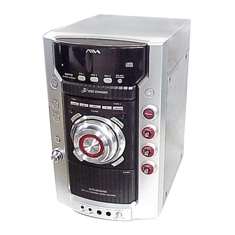
Photo : CX-JDS50
Model Name Using Similar Mechanism
CD
CD Mechanism Type
Section
Optical Pick-up Name
Model Name Using Similar Mechanism
TAPE
Section
Tape Transport Mechanism Type
SPECIFICATIONS
JDS20
DIN power output (rated): 96 + 96 watts (6 ohms at
1 kHz, DIN)
Continuous RMS power output (reference):
120 + 120 watts (6 ohms at
1 kHz, 10% THD)
Music power output (reference):
180 + 180 watts (6 ohms at
1 kHz, 10% THD)
Other models:
JDS50
The following measured at AC 120, 127, 220, 240 V
50/60 Hz
DIN power output (rated): 160 + 160 watts (6 ohms at
1 kHz, DIN)
Continuous RMS power output (reference):
200 + 200 watts (6 ohms at
1 kHz, 10% THD)
COMPACT DISC DECK RECEIVER
AEP Model
E Model
CX-JDS20/JDS50
Australian Model
Russian Model
CX-JDS20/JDS50
NEW
BU-F1BD81A
KSM-215DCP/C2NP
CX-LEM330
JDS20
CMAL5Z220A
JDS50
CMAL1Z240A
JDS20
The following measured at AC 120, 127, 220, 240 V
50/60 Hz
DIN power output (rated): 96 + 96 watts (6 ohms at
1 kHz, DIN)
Continuous RMS power output (reference):
120 + 120 watts (6 ohms at
1 kHz, 10% THD)
Inputs
AUDIO IN (stereo mini jack):
voltage :
JDS20: 1.85 V
JDS50: 0.9 V,
impedance 47 kilohms
MIC (phone jack) (except for European model):
se
nsitivity:
JDS20: 0.25 mV
JDS50: 0.1 mV,
impedance 10 kilohms
Outputs
PHONES (stereo mini jack):
accepts headphones of
8 ohms or more
SPEAKER:
accepts impedance of 6 to
16 ohms
— Continued on next page —
CX-JDS20
CX-JDS20
Advertisement
Table of Contents

Related Manuals for Aiwa CX-JDS20


Summary of Contents for Aiwa CX-JDS20
- Page 1 Ver. 1.0 2005.03 E Model CX-JDS20/JDS50 Australian Model CX-JDS20 Russian Model CX-JDS20/JDS50 CX-JDS20/JDS50 are the Amplifier, CD player, Tape Deck and Tuner section in DBX-DS20/DBX-DS50. Photo : CX-JDS50 Model Name Using Similar Mechanism CD Mechanism Type BU-F1BD81A Section Optical Pick-up Name...
- Page 2 CX-JDS20/JDS50 CD player section General System Compact disc and digital Power requirements audio system European and Russian models: 230 V AC, 50/60 Hz Laser Diode Properties Emission duration: continuous Australian model: 230 – 240 V AC, 50/60 Hz Laser Output: Less than...
- Page 3 CX-JDS20/JDS50 NOTES ON HANDLING THE OPTICAL PICK-UP The release method of a CD disc tray LOCK function BLOCK OR BASE UNIT There is a disc lock function for the disc theft prevention for a The laser diode in the optical pick-up block may suffer electrostatic demonstration at a shop front in this machine.
-
Page 4: Table Of Contents
CX-JDS20/JDS50 TABLE OF CONTENTS GENERAL 6-4. Printed Wiring Board – MAIN (JDS20) Section – ..26 ..............5 6-5. Printed Wiring Board – MAIN (JDS50) Section – ..27 6-6. Schematic Diagram – MAIN Section (1/2) – ....28 DISASSEMBLY 6-7. -
Page 5: General
CX-JDS20/JDS50 SECTION 1 GENERAL This section is extracted from instruction manual. List of button locations and reference pages How to use this page Illustration number Use this page to find the location of buttons and other TUNER/BAND wh (14, 15) parts of the system that are mentioned in the text. -
Page 6: Setting The Clock
CX-JDS20/JDS50 Remote control ALPHABETICAL ORDER BUTTON DESCRIPTIONS ?/1 (power) 1 (7, 24) A – E F – Z m/M (rewind/fast forward) CD qk (9, 12) FM MODE 4 (16) 7 (10, 17) CLEAR qg (13) FOLDER + qa (10, 12, 18) -
Page 7: Disassembly
CX-JDS20/JDS50 SECTION 2 DISASSEMBLY 2-1. DISASSEMBLY FLOW • This set can be disassembled in the order shown below. 2-2. TOP PANEL, SIDE PANEL 2-15. CASSETTE PANEL (Page 8) (Page 15) 2-3. FRONT SECTION (Page 8) 2-4. CD MECHANISM SECTION 2-6. DS-PANEL BOARD... -
Page 8: Top Panel, Side Panel
CX-JDS20/JDS50 Note: Follow the disassembly procedure in the numerical order given. 2-2. TOP PANEL, SIDE PANEL 6 left panel 5 two screws qa top panel (+BVTP 3 × 10) 7 three screws (+BVTP 3 × 10) 4 four screws (Case 3) -
Page 9: Cd Mechanism Section
CX-JDS20/JDS50 2-4. CD MECHANISM SECTION 2 CD mechanism section 1 two screws (+BVTP)(B3) 2-5. CASSETTE MECHANISM DECK, DS-PAI/HP/MIC BOARD 4 cassette mechanism deck 2 wire (flat type) (8core) 3 three screws (+PTP)(B2.6) 6 holder (PWB MIC) 1 three screws (+PTP)(B2.6) -
Page 10: Ds-Panel Board
CX-JDS20/JDS50 2-6. DS-PANEL BOARD 1 knob (RTRY) 3 knob (RTRY AMS) 6 DS-PANEL board 2 guide (LED VOL) 4 twenty screws (+PTP)(B2.6) 3 connector (11p) (CN651) 2-7. REAR CABINET 4 rear cabinet 1 connector (2p) (CN871) 3 four screws 2 wire (flat type) -
Page 11: Power Trans
CX-JDS20/JDS50 2-8. POWER TRANS 1 four screws 3 power trans 2 cord bushing 2-9. DS-MAIN BOARD, HEAT SINK 3 screw (+BVTP)(B3) 6 heat sink 4 connector 5 DS-MAIN board 1 two screws 2 two screws (+BVTP)(B3) (+BVTP)(B3) -
Page 12: Holder (Cd Mech)
CX-JDS20/JDS50 2-10. HOLDER (CD MECH) 1 four s crews (+BVTP 2.6 × 8) 5 s crew (+BVTP 2.6 × 8) 6 DS CONN board 3 tape 7 holder (CD MECH) 2 wire (flat type) (27 core) (CN606) 4 wire (flat type) (27 core) 2-11. -
Page 13: Bd Board, Optical Pick-Up (Ksm-215Dcp/C2Np)
CX-JDS20/JDS50 2-12. BD BOARD, OPTICAL PICK-UP (KSM-215DCP/C2NP) 1 s crew (+BVTP 2.6 × 8) 2 gap tube 5 B D board 4 Remove the four solderings of motor. 3 wire (flat type) (16 core) 7 two insulators 6 two insulators... -
Page 14: Belt
CX-JDS20/JDS50 2-14. BELT 2 Slide the upper-most tray foward the front. 1 Release the hook of the tray. 4 two belts 3 While pushing up the plate cam, d raw the Drawer (three trays) entirely foward front. plate cam... -
Page 15: Cassette Panel
CX-JDS20/JDS50 2-15. CASSETTE PANEL 3 two claws 2 Open the 1 Push the cassette panel. cassette panel. 4 cassette panel... -
Page 16: Test Mode
CX-JDS20/JDS50 SECTION 3 TEST MODE [COLD RESET] [Disc Tray Lock] The cold reset clears all data including preset data stored in The disc tray lock function for the antitheft of an demonstration the RAM to initial conditions. Execute this mode when disc in the store is equipped. -
Page 17: Mechanical Adjustments
CX-JDS20/JDS50 SECTION 4 SECTION 5 MECHANICAL ADJUSTMENTS ELECTRICAL ADJUSTMENTS TAPE MECHANISM DECK SECTION DECK SECTION 0 dB=0.775V Precaution 1. Clean the following parts with a denatured alcohol-moistened Precaution swab: 1. Demagnetize the record/playback head with a head record/playback heads pinch rollers demagnetizer. - Page 18 CX-JDS20/JDS50 Record Bias Adjustment 3. Mode: Playback DS-MAIN board Procedure: SPEAKER terminal (J171) test tape L-CH P-4-A100 1. Record mode oscilloscope (10 kHz, –10 dB) DS-MAIN board L-CH AUX IN (J552) 1) 315 Hz 50 mV (–23.8 dB) 2) 10 kHz ...
- Page 19 CX-JDS20/JDS50 RFDC signal waveform CD SECTION VOLT/DIV: 200 mV TIME/DIV: 500 ns Note: 1. Use YEDS-18 disc (3-702-101-01) unless otherwise indicated. 2. Use an oscilloscope with more than 10MΩ impedance. 3. Clean the object lens by an applicator with neutral detergent level: 0.6 ±...
- Page 20 CX-JDS20/JDS50 E-F Balance Adjustment Checking Location: Connection: – BD BOARD (Side B) – oscilloscope BD board TP (TEO) TP (VC) – IC303 Procedure: 1. Connect an oscilloscpe to test point TP (TEO) and TP (VC) on the BD board. 2. Set the FUNCTION to “CD”.
-
Page 21: Diagrams
CX-JDS20/JDS50 SECTION 6 DIAGRAMS • Circuit Boards Location THIS NOTE IS COMMON FOR PRINTED WIRING BOARDS AND SCHEMATIC DIAGRAMS. (In addition to this, the necessary note is printed in each block.) For Schematic Diagrams. For Printed Wiring Boards. Note: Note: •... -
Page 22: Block Diagram - Main Section
CX-JDS20/JDS50 6-1. BLOCK DIAGRAM – MAIN SECTION – J552 IC301 (IC201) AUDIO IN POWER AMP SELECTOR IC401 R-CH R-CH J551 AUX-L OUT-L 11 LI+ PHONES Q301 OUT-R R-CH (Q201) 14 LI+ OVERLOAD PBIP JDS50 JDS50 RY171 Q264,265 TUNER PACK REC10... -
Page 23: Bd Section
CX-JDS20/JDS50 – BD SECTION – OPTICAL PICK-UP BLOCK (KSM-215DCP/C2NP) DETECTOR IC301 DIGITAL SIGNAL IC101 +1.7V RF AMP PROCESSOR +3.3V IC303 PCMD1 SDO0 3.3V LRCK1 LRCKIA LRCK SFSY/LRCK1B VDDM PCMD SDIO IC604(2/2) BCKIA SYSTEM CONTROLLER BCK1 SBSY/BCK1B MP3STB MP3REQ DRIVER MIACK... -
Page 24: Printed Wiring Board - Bd Section
CX-JDS20/JDS50 • See page 21 for Circuit Boards Location. 6-2. PRINTED WIRING BOARD – BD SECTION – :Uses unleaded solder. • Semiconductor Location Ref. No. Location IC101 IC251 IC301 IC303 SPINDLE MOTOR IC303 S101 (LIMIT) SLED IC301 MOTOR IC251 (VC) -
Page 25: Schematic Diagram - Bd Section
CX-JDS20/JDS50 • See page 42 for IC Block Diagrams. • See page 44 for IC Pin Function Description. 6-3. SCHEMATIC DIAGRAM – BD SECTION – CN101 R307 C134 C125 C307 TP304 TP423 IOP1 TP10 TP11 C151 100k TP424 IOP2 TP12... -
Page 26: Printed Wiring Board - Main (Jds20) Section
CX-JDS20/JDS50 • See page 21 for Circuit Boards Location. 6-4. PRINTED WIRING BOARD – MAIN (JDS20) SECTION – :Uses unleaded solder. TUNER REC/PB EXCEPT AUS EXCEPT AEP ERASE HEAD (REC/PB/ERASE) AEP,RU,AUS FFC802 AEP,RU,AUS FFC801 IC401 DS-PANEL BOARD CN601 (page 30) -
Page 27: Printed Wiring Board - Main (Jds50) Section
CX-JDS20/JDS50 • See page 21 for Circuit Boards Location. 6-5. PRINTED WIRING BOARD – MAIN (JDS50) SECTION – :Uses unleaded solder. TUNER REC/PB EXCEPT AUS ERASE HEAD (REC/PB/ERASE) FFC802 IC401 DS-PANEL BOARD CN601 C449 (page 30) EXCEPT AEP • Semiconductor Location Ref. -
Page 28: Schematic Diagram - Main Section (1/2)
CX-JDS20/JDS50 6-6. SCHEMATIC DIAGRAM – MAIN SECTION (1/2) – FFC801 R851 4.7k R857 4.7k R854 R803 R802 JR801 JR802 C804 R810 R811 R812 R813 R801 R814 M871 FFC802 11P P1.25 FAN MOTOR CNP871 D801 R804 MC2840 4.7k R885 FAN MOTOR... -
Page 29: Schematic Diagram - Main Section (2/2)
CX-JDS20/JDS50 • See page 42 for IC Block Diagram. 6-7. SCHEMATIC DIAGRAM – MAIN SECTION (2/2) – CN101 TYK30P BOARD TO BOARD JW102 C120 2200 10V D124 D117 D118 D119 10EDB40-TB5 10EDB40-TB5 10EDB40-TB5 10EDB40-TB5 R501 R407 C405 C431 1000p C451... -
Page 30: Printed Wiring Board - Panel (Jds20/Jds50) Section
CX-JDS20/JDS50 • See page 21 for Circuit Boards Location. 6-8. PRINTED WIRING BOARD – PANEL (JDS20/JDS50) SECTION – :Uses unleaded solder. FL601 (FLUORESCENT INDICATOR TUBE) • Semiconductor MECHANISM Location DECK IC602 Ref. No. Location D601 D602 D603 IC601 D604 D605... -
Page 31: Schematic Diagram - Panel Section (1/2)
CX-JDS20/JDS50 • See page 21 for Waveforms. • See page 47 for IC Pin Function Description. 6-9. SCHEMATIC DIAGRAM – PANEL SECTION (1/2) – FFC602 R676 R654 R655 R656 IC602 R678 JR604 RPM7240-H18 R797 C642 Q611 2SA1365EF Q612 2SA1365EF R672... -
Page 32: Schematic Diagram - Panel Section (2/2)
CX-JDS20/JDS50 • See page 43 for IC Block Diagram. 6-10. SCHEMATIC DIAGRAM – PANEL SECTION (2/2) – FL601 HNA-09SS59T -0824 C614 C615 C616 LED608 LED607 I-BASS STBY R734 SLR325-VCT31 SLR325-VCT31 R652 R628 R653 Q630 R805 2SA1115TP 2.2k R776 R786 R787... -
Page 33: Printed Wiring Board - Panel Comb (Jds20) Section
CX-JDS20/JDS50 • See page 21 for Circuit Boards Location. 6-11. PRINTED WIRING BOARD – PANEL COMB (JDS20) SECTION – :Uses unleaded solder. DS-PANEL BOARD CN651 VOLUME (page 30) BOARD CN201 (page 24) LED601-606 ILUMINATION DS-MAIN BOARD(JDS20) CN112(11P) (page 26) EXCEPT AEP... -
Page 34: Printed Wiring Board - Panel Comb (Jds50) Section
CX-JDS20/JDS50 • See page 21 for Circuit Boards Location. 6-12. PRINTED WIRING BOARD – PANEL COMB (JDS50) SECTION – :Uses unleaded solder. DS-PANEL BOARD CN651 VOLUME (page 30) BOARD CN201 LED601-606 ILUMINATION (page 24) 1-865-368- DS-MAIN BOARD(JDS50) CN112(11P) (page 27) -
Page 35: Schematic Diagram - Panel Comb Section
CX-JDS20/JDS50 6-13. SCHEMATIC DIAGRAM – PANEL COMB SECTION – S652 R746 CN606 CN605 R754 R799 R800 R783 R719 RTRY VOLUME R720 R748 R747 4.7k R798 R755 R756 R718 R784 R785 R750 R749 2.2k R751 220k R752 LED604 LED603 LED602 LED601 R753 2.2k... -
Page 36: Printed Wiring Board - Amp (Jds20) Section
CX-JDS20/JDS50 • See page 21 for Circuit Boards Location. 6-14. PRINTED WIRING BOARD – AMP (JDS20) SECTION – :Uses unleaded solder. • Semiconductor Location Ref. No. Location D361 D362 D363 IC301 Q301 Q302 Q303 IC301 Q304 Q305 Q306 Q361 Q362... -
Page 37: Printed Wiring Board - Amp (Jds50) Section
CX-JDS20/JDS50 • See page 21 for Circuit Boards Location. 6-15. PRINTED WIRING BOARD – AMP (JDS50) SECTION – :Uses unleaded solder. • Semiconductor Location Ref. No. Location D261 D262 D263 IC201 Q201 Q202 IC201 Q203 Q204 Q205 Q206 Q261 Q262... -
Page 38: Schematic Diagram - Amp (Jds20) Section
CX-JDS20/JDS50 6-16. SCHEMATIC DIAGRAM – AMP (JDS20) SECTION – Q303 C307 R307 2SC3052EF Q361 C308 2SC3052EF Q304 R308 Q362 2SC305E2F R365 2SA1235F R319 4.7k 4.7k R320 EP301 4.7k EARTH,PLATE R317 R315 R313 Q305 R350 JR301 2SA1235F R310 R304 R363 R364 2.2k... -
Page 39: Schematic Diagram - Amp (Jds50) Section
CX-JDS20/JDS50 6-17. SCHEMATIC DIAGRAM – AMP (JDS50) SECTION – Q203 2SC3052EF C207 C208 R265 R207 R208 R219 R220 Q204 R260 R264 Q261 4.7k 4.7k 2SC3052EF R213 R215 2.2k 2.2k R217 R212 2SC3052EF R210 R250 Q263 C213 Q262 2SA1514K 10p 50V... -
Page 40: Printed Wiring Board - Power (Jds20/Jds50) Section
CX-JDS20/JDS50 • See page 21 for Circuit Boards Location. 6-18. PRINTED WIRING BOARD – POWER (JDS20/JDS50) SECTION – :Uses unleaded solder. AC IN AC IN EXCEPT MX,AUS EXCEPT MX EXCEPT EXCEPT MX,AUS E51,AUS MX,AUS S001 S001 VOLTAGE VOLTAGE MX, AEP,RU... -
Page 41: Schematic Diagram - Power Section
CX-JDS20/JDS50 6-19. SCHEMATIC DIAGRAM – POWER SECTION – MX, AUS T002 T001 CN001 1P TERMINAL 1P TERMINAL RY001 JW024 JW018 JW007 WH002 WIRE,HLDR JW020 JW019 JW017 JW021 S001 SW,SL 1-2-3 SWS2301 WH001 WIRE,HLDR JW009 JW008 JW010 C005 C004 PT003 SUB PT... - Page 42 CX-JDS20/JDS50 • IC Block Diagrams IC251 BA5947FM — BD Board — IC301 TA94A34FG-002 CH1PUTF CH4OUTR CH1OUTR CH4OUTF CH2OUTF CH3OUTF LRCKIA PIN26 6.5k CH3OUTR CH2OUTR Vref POWVCC POWVCC BCKIA (ch3, 4) (ch1, 2) 50k 50k 50k 50k MUTE CNF4 50k 50k...
- Page 43 CX-JDS20/JDS50 — DS-PANEL Board — IC601 uPD163315GB-3BS Grid driver Multiplexed driver SEG19/GRID10 Command decoder LED1 SEG18/GRID11 LED2 Display memory LED3 SEG17/GRID12 24 bits x 12 words LED4 Timing generator key scan DOUT SEG16/KS16 Key data memory Serial SEG15/KS15 (2 x 16 bits)
- Page 44 CX-JDS20/JDS50 • IC Pin Function Description BD BOARD IC101 CXD3059AR (RF AMP) Pin No. Pin Name Description MIRR Mirror signal input/output (Not used) DFCT Defect signal input/output (Not used) Focus OK signal input/output (Not used) — Internal digital ground GFS is sampled at 460Hz; when GFS is high , this pin outputs a high signal...
- Page 45 CX-JDS20/JDS50 Pin No. Pin Name Description VPCO Wide-band EFM PLL charge pump output VCTL Wide-band EFM PLL VCO2 control voltage input AVSS3 — Analog ground CLTV Multiplier VCO1 control voltage input FILO Master PLL (slave = digital PLL) filter output...
- Page 46 CX-JDS20/JDS50 Pin No. Pin Name Description SQSO Subcode Q 80-bit and PCM peak and level data output CD TEXT data output SQCK SQSO readout clock input SBSO Subcode P to W serial output EXCK SBSO readout clock input XRST System reset Reset when low...
- Page 47 CX-JDS20/JDS50 DS-PANEL BOARD IC604 M30302MCP-A04FPU0 (SYSTEM CONTROLLER) Pin No. Pin Name Description Solenoid control signal output to the tape deck PLAY switch signal input from the tape deck Record protect detect switch signal input (rear) Record protect detect switch signal input (f)
- Page 48 CX-JDS20/JDS50 Pin No. Pin Name Description CD motor drivel signal output (–M2) CD motor drive signal output (+M1) O-MILP Latch pulse signal output to the MP3 IC O-MP3STBY Strobe signal output to the MP3 IC CD motor drive signal output (–M1)
- Page 49 CX-JDS20/JDS50 Pin No. Pin Name Description AVSS — Ground terminal P100/AN0 Volume signal input from the rotary encoder VREF Reference voltage AVCC — Power supply terminal (+3.3V) Motor control signal output to the tape deck...
-
Page 50: Exploded Views
CX-JDS20/JDS50 SECTION 7 EXPLODED VIEWS NOTE: • -XX and -X mean standardized parts, so they • The mechanical parts with no reference The components identified by mark 0 or may have some difference from the original number in the exploded views are not supplied. -
Page 51: Front Section
CX-JDS20/JDS50 7-2. FRONT SECTION supplied supplied supplied supplied supplied supplied supplied supplied Ref. No. Part No. Description Remark Ref. No. Part No. Description Remark 2-515-182-01 REFLECTOR (VOL) A-1101-547-A DS-PANEL BOARD, COMPLETE 3-254-151-01 SCREW (B2.6), (+) P TAPPING (including DS-CONN BOARD) (AEP) -
Page 52: Chassis Section
CX-JDS20/JDS50 7-3. CHASSIS SECTION supplied supplied supplied PT001 PT002 supplied supplied supplied Ref. No. Part No. Description Remark Ref. No. Part No. Description Remark 3-254-142-01 SCREW (B3), (+) BV TAPPING 0 106 1-830-384-11 CORD, POWER (AEP, E51, RU) 2-515-258-01 HOLDER (MAIN) -
Page 53: Cd Mechanism Section-1
CX-JDS20/JDS50 7-4. CD MECHANISM SECTION-1 CD MECHANISM SECTION-2 supplied DS-CONN board including Ref. No. 68 including Ref. No. 67 Ref. No. Part No. Description Remark Ref. No. Part No. Description Remark 0 157 3-254-151-01 SCREW (B2.6), (+) P TAPPING 8-820-244-01 OPTICAL PICK-UP KSM-215DCP/C2NP... -
Page 54: Cd Mechanism Section-2
CX-JDS20/JDS50 7-5. CD MECHANISM SECTION-2 supplied supplied supplied Ref. No. Part No. Description Remark 1-797-193-11 MECH, CD (BU-F1BD81C) 2-632-062-01 BELT (DLM3A) -
Page 55: Electrical Parts List
CX-JDS20/JDS50 SECTION 8 ELECTRICAL PARTS LIST NOTE: • Due to standardization, replacements in the • COILS When indicating parts by reference number, uH: µH parts list may be different from the parts please include the board name. specified in the diagrams or the components •... - Page 56 CX-JDS20/JDS50 DS-AMPLIFIER (403) Ref. No. Part No. Description Remark Ref. No. Part No. Description Remark < TRANSISTOR > R410 1-216-809-11 METAL CHIP 1/10W R411 1-216-809-11 METAL CHIP 1/10W 6-551-120-01 TRANSISTOR 2SA2119K R412 1-216-809-11 METAL CHIP 1/10W < RESISTOR > R419...
- Page 57 CX-JDS20/JDS50 DS-AMPLIFIER (403) DS-AMPLIFIER (412) Ref. No. Part No. Description Remark Ref. No. Part No. Description Remark JR303 1-216-864-11 SHORT CHIP R348 1-216-837-11 METAL CHIP 1/10W R349 1-216-864-11 SHORT CHIP < TRANSISTOR > R350 1-216-841-11 METAL CHIP 1/10W Q301 6-551-270-01 TRANSISTOR...
- Page 58 CX-JDS20/JDS50 DS-AMPLIFIER (412) Ref. No. Part No. Description Remark Ref. No. Part No. Description Remark C260 1-164-156-11 CERAMIC CHIP 0.1uF R216 1-216-837-11 METAL CHIP 1/10W C261 1-164-156-11 CERAMIC CHIP 0.1uF R217 1-216-864-11 SHORT CHIP C262 1-110-518-91 ELECT 10uF 100V R218...
- Page 59 CX-JDS20/JDS50 DS-AMPLIFIER (412) DS-CONN DS-MAIN Ref. No. Part No. Description Remark Ref. No. Part No. Description Remark R274 1-216-837-11 METAL CHIP 1/10W C105 1-127-813-11 ELECT 3300uF R275 1-216-833-11 METAL CHIP 1/10W (JDS20: MX, E51, AUS) R276 1-216-813-11 METAL CHIP 1/10W...
- Page 60 CX-JDS20/JDS50 DS-MAIN Ref. No. Part No. Description Remark Ref. No. Part No. Description Remark C413 1-162-970-11 CERAMIC CHIP 0.01uF C414 1-162-970-11 CERAMIC CHIP 0.01uF C528 1-162-970-11 CERAMIC CHIP 0.01uF C415 1-162-970-11 CERAMIC CHIP 0.01uF C529 1-126-964-11 ELECT 10uF C530 1-162-966-11 CERAMIC CHIP 0.0022uF 10%...
- Page 61 CX-JDS20/JDS50 DS-MAIN Ref. No. Part No. Description Remark Ref. No. Part No. Description Remark D157 8-719-000-07 DIODE MC2836 < RESISTOR > D158 6-500-848-01 DIODE MC2840-T112-1 D401 8-719-083-60 DIODE UDZSTE-174.7B R101 1-216-837-11 METAL CHIP 1/10W D402 8-719-083-60 DIODE UDZSTE-174.7B (JDS20) R101...
- Page 62 CX-JDS20/JDS50 DS-MAIN Ref. No. Part No. Description Remark Ref. No. Part No. Description Remark R136 1-260-328-11 CARBON 1/2W R183 1-260-328-11 CARBON 1/2W (JDS50) (JDS50) R137 1-259-296-11 CARBON 1/2W R184 1-259-296-11 CARBON 1/2W (JDS20) (JDS20) R185 1-249-657-31 CARBON 1/2W R137 1-260-328-11 CARBON...
- Page 63 CX-JDS20/JDS50 DS-MAIN Ref. No. Part No. Description Remark Ref. No. Part No. Description Remark R440 1-216-825-11 METAL CHIP 2.2K 1/10W R534 1-216-833-11 METAL CHIP 1/10W R441 1-216-829-11 METAL CHIP 4.7K 1/10W R442 1-216-829-11 METAL CHIP 4.7K 1/10W R535 1-216-825-11 METAL CHIP 2.2K...
- Page 64 CX-JDS20/JDS50 DS-MAIN DS-PAI/HP/MIC Ref. No. Part No. Description Remark Ref. No. Part No. Description Remark < RELAY > J552 1-794-702-11 JACK, HEADPHONE (AUDIO IN) J553 1-770-226-11 JACK (LARGE TYPE) (MIC1) (EXCEPT AEP) RY171 1-755-170-11 RELAY (12V) J554 1-770-226-11 JACK (LARGE TYPE) (MIC2) (EXCEPT AEP) <...
- Page 65 CX-JDS20/JDS50 DS-PAI/HP/MIC DS-PANEL Ref. No. Part No. Description Remark Ref. No. Part No. Description Remark R580 1-216-813-11 METAL CHIP 1/10W C638 1-162-964-11 CERAMIC CHIP 0.001uF (EXCEPT AEP) C640 1-162-962-11 CERAMIC CHIP 470PF C641 1-164-156-11 CERAMIC CHIP 0.1uF < VARIABLE RESISTOR >...
- Page 66 CX-JDS20/JDS50 DS-PANEL Ref. No. Part No. Description Remark Ref. No. Part No. Description Remark < FLUORESCENT INDICATOR > Q629 8-729-024-43 TRANSISTOR 2SA1365-T112-1EF Q630 8-729-119-76 TRANSISTOR 2SA1175-HFE FL601 1-519-820-11 INDICATOR TUBE, FLUORESCENT Q631 8-729-047-62 TRANSISTOR 2SC3440-T12-1F < IC > < RESISTOR >...
- Page 67 CX-JDS20/JDS50 DS-PANEL Ref. No. Part No. Description Remark Ref. No. Part No. Description Remark R634 1-216-809-11 METAL CHIP 1/10W R690 1-216-821-11 METAL CHIP 1/10W R635 1-216-821-11 METAL CHIP 1/10W R691 1-216-857-11 METAL CHIP 1/10W R636 1-216-833-11 METAL CHIP 1/10W R692...
- Page 68 CX-JDS20/JDS50 DS-PANEL DS-POWER Ref. No. Part No. Description Remark Ref. No. Part No. Description Remark R767 1-216-817-11 METAL CHIP 1/10W S624 1-771-410-21 SWITCH, TACTILE (TUNER/BAND) R768 1-216-809-11 METAL CHIP 1/10W S625 1-771-410-21 SWITCH, TACTILE (EQ) R769 1-216-821-11 METAL CHIP 1/10W...
- Page 69 CX-JDS20/JDS50 DS-VOL Ref. No. Part No. Description Remark Ref. No. Part No. Description Remark DS-VOL BOARD 0 PT002 1-443-698-11 TRANSFORMER, POWER (JDS50: E51) 0 PT002 1-443-702-11 TRANSFORMER, POWER (JDS20: E51, AUS) ************* < LED > LED601 6-500-641-01 DIODE SLI-325URC LED602 6-500-641-01 DIODE SLI-325URC...
-
Page 70: Revision History
CX-JDS20/JDS50 REVISION HISTORY Clicking the version allows you to jump to the revised page. Also, clicking the version at the upper right on the revised page allows you to jump to the next revised page. Ver. Date Description of Revision...