
Related Manuals for Sharp LC-26D44


Summary of Contents for Sharp LC-26D44
- Page 1 Training Course MODELS: LC-26D44 LC-32D44 Presentation By: Issued: Sofía García Jan Niemi SEES Engineering Department May 2008 Training course: D44 SEES Engineering Department...
- Page 2 Index 1. Models introduction 2. Block Diagram 3. Software Updating 4. Service Mode 5. LCD Adjust Process 6. Electrical Diagrams / PWB Training course: D44 SEES Engineering Department...
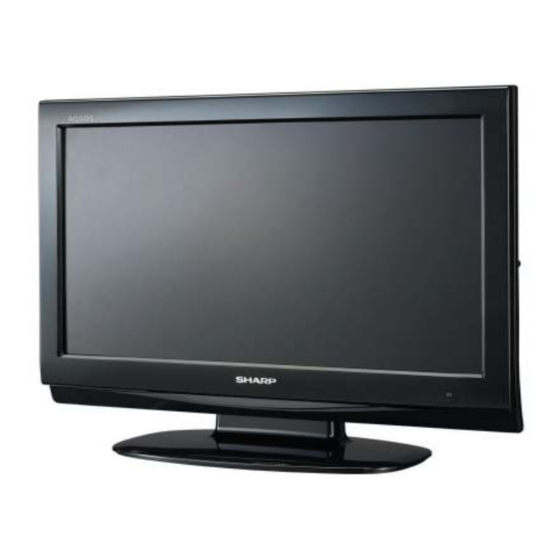
- Page 3 1. Models Introduction Sizes: 26” & 32” Type of cabinet: - Bottom speakers. - BK : Black Color. - GY: Grey Color. Models: LC-26/32D44EE-BK/GY → Continental LC-26/32D44ES-BK/GY → Sweden Market LC-26/32D44EK-BK/GY → United Kingdom LC-26/32D44RU-BK/GY → Russian Market Training course: D44 SEES Engineering Department...
- Page 4 0°C to k40°C • Active Backlight (dynamic contrast 10.000:1) • As a part of policy of continuous improvement, SHARP reserves the right to make design and specification changes for • Sleep Timer. product improvement without prior notice. The performance specification figures indicated are nominal values of production units.
-
Page 5: Block Diagrams
IC1951: HDMI RECEIVER (High Defi nition Multimedia Interface) Part number : Sii9025 SHARP Code : VHISII9025+-1Q The Sii9025 is a compliant with the latest HDMI 1.2 (High Defi nition Multimedia Interface) specifi cation. Backward compatibility with DVI 1.0 allows HDMI systems to connect to existing DVI 1.0 hosts. The SiI9025 is capable of receiving and outputting two channel digital audio at up to 192 kHz- an excellent solution for Digital TVs. - Page 6 IC1922 & IC1902: NVM OF HDMI (E-EDID) Part Number : 24LC2BIN SHARP Code: VHI24LC2BIN-1Y This IC is a 2-wire (I2C bus type) serial EEPROM this is electrically programmable. This EEPROM chip stores the data structure used to carry confi guration information for optimal use of a display (EDID data).
- Page 7 IC4252: NVM 64Kb-E2PROM FOR DIGITAL PROCESSOR (IC4001). Part Number : BR24S64FVM-WTR SHARP Code: VHIBR24S64M-1Y The BR24S64FVM is a 2-wire (I2C bus type) serial EEPROM that is electrically programmable. This IC stores all data related to the Digital Module (Channels, User settings, etc.).
- Page 8 IC3001: Main CPU / VIDEO PROCESSOR. Part Number: VCT7993P-FA-A1-H000 SHARP Code: RH-IXC354WJZZQ The VCT 77VWP (VCT-Pro) family is dedicated to high-quality FPD and double-scan TV sets. The memory and program ROM are integrated in the IC. Modular design and deep submicron technology allow the integration of audio, video, Teletext, OSD, and controller-related functionalities.
- Page 9 IC3051: NVM 64Kb-E2PROM FOR ANALOG PROCESSOR (IC3001). Part Number: BR24S64FVM-WTR SHARP Code: VHIBR24S64M-1Y The BR24S64FVM is a 2-wire (I2C bus type) serial EEPROM that is electrically programmable. This IC stores all data related to the Analog Module (Channels, User settings, etc.) IC2302: SUB-CPU AND PORT EXPANSOR.
- Page 10 VHIT3Z18AFG-1Q This IC is a custom Gate Array of Toshiba. The alias of this IC is EAGLE2 and is marked as SHARP. This IC is generating all the necessary timing signals for controlling the panel and the RSDS interface for data..
- Page 11 IC203: I2C BUS SELECTOR Part Number: SN74LV4053APWR SHARP Code: VHILV4053AT-1Y The SN74LV4053APWR is a high-speed CMOS analog multiplexer/demultiplexer backed by silicon gate CMOS technology. The multiplexer func- tion includes the selection and mixing of analog and digital signals. The chip includes two independent 3 channels selectors. A digital signal through the control terminal turns on the switch of a corresponding channel.
- Page 12 2. Block Diagrams (continued) Overall Wiring Diagram 26” Training course: D44 SEES Engineering Department...
- Page 13 RUNTKA395WJQZ Power Supply & Inverter Block Diagram (26”) STB, OFL1,OSC, Dimming Control, REG,REG2,BRT,ADIM Other I/O signal Comments Comments Feedback, Lamp Open & Shorted Protections Power Block High Current path Signal path 1 2 Transformer Signal Block Controller ON/OFF switch CCFL High Voltage IC7500 1 2 Transformer...
- Page 14 2. Block Diagrams (continued) RUNTKA396WJQZ Power Supply Block Diagram (32”) PS_ON HALF BRIDGE Nº 1 CURRENT SENSOR Nº2 60/13V REG 60/13V OVERVOLTAGE 13V OVERVOLT. PS_ON AC DET BU+5V REG 60V OVERVOLT. 13V SHORT DET STBY ON/UNDERV. Training course: D44 SEES Engineering Department...
- Page 15 2. Block Diagrams (continued) RUNTKA396WJQZ Inverter Block Diagram (32”) SHORT CIRCUIT PROTECTION HIGH CURRENT LAMP TIMER LATCH LOW VOLT LAMP C7558=GROUND PROT DISABLED LAMP OPEN Training course: D44 SEES Engineering Department...
-
Page 16: Software Updating
3. Software Updating HOW TO UPDATE THE SOFTWARE VCTPro SOFTWARE UPDATE There are 4 methods to update software in the VCTpro: • RS-232C HyperTerminal Method • RS-232C Tera Term Method NOTE: (RS-232C method is allowed when the TV is working properly and the action should be only software upgrade) •... -
Page 17: Service Mode
4. Service Mode HOW TO ENTER TO SERVICE MODE • Press the “POWER” key on the set of running TV set to force off the power. • While holding down the “VOL (-)” and “INPUT” keys on the set at once, plug in the AC power cord to turn on the power. The letter “K”, appears on the screen. - Page 18 4. Service Mode (continued) Display Description The colors of K letter that shown on the screen when TV is at Inspection Mode are as follows: Picture adjustment: without making adjustments. (SRC or after delete NVM ) Grey Picture adjustment is doing. (SEES) Light Blue All picture adjustments have been completed.
- Page 19 4. Service Mode (continued) Service Mode Menu The character string in brackets [ ] will appear as a page title in the adjustment process menu header. Page Line Item Description Remarks (Adjustment detail, etc.) [M GAMMA 1-3] 8/11 [INFO] MGAMMA R 1 W/B adjustment, gradation 1R adjustment value 1/11 MGAMMA G 1...
- Page 20 5. LCD Adjustment Process TUNER LEVEL ADJUSTMENT Adjustment Point Adjustment Conditions Adjustment Point Settings [Signal] Feed the PAL color bar signal (E-12CH) to TUNER. Sig- RF Signal nal level: 55 ± 1dB μV (75Ω LOAD) [TUNER] ↑ 100% white Auto adjustment Adjustment Process (See Bring the cursor on [TUNER ADJ] and press [OK].
- Page 21 5. LCD Adjustment Process (continued) W/B ADJUSTMENT FROM PC Lista de comandos RS-232C 1- Get ready the PC with COM port (RS-232C) running on Windows 95/98/ Command Function Remarks ME/2000/XP operating system, as well as the RS-232C cross cable. KYOF0000 Remote control disabled OSDS0001 OSD display inhibited...
-
Page 22: Hotel Mode
5. LCD Adjustment Process (continued) HOTEL MODE How to Enter in the Public Mode (Hotel Mode) Public Mode There are three following ways to display the Public Mode setting screen. POWER ON FIXED [VARIABLE] 1- On the process adjustment mode screen (2/33), set the “HOTEL MODE” Flag to ON. MAXIMUM VOLUME [60] Turn off the power, and turn it on again, pressing the CH▲... - Page 23 5. LCD Adjustment Process (continued) Public Mode Settings POWER ON FIXED [VARIABLE FIXED] When it is set to “FIXED” the TV is impossible to be switch off by Main Switch or Remote Control. MAXIMUM VOLUME Is possible to set the maximum volume at limited level. VOLUME FIXED [VARIABLE FIXED]...
-
Page 24: Electrical Diagrams
6. Electrical Diagrams Main 1/13 (TUNER.OFDM) Schematic Diagram TL212 TL202 C1035 R1010 FB1031 3.9K A188WJ P1001 5.18 5.18 5.18 MA012WJ KZA510WJPZ TL1001 TU201 L263 5.12 5.18 5.18 AA019WJQZ S_PLG 12uH C1017 TL1002 R1006 C1005 C1007 0.1u VIDEO-OUT IF-AGC IF(D2) IF(D1) R1033 6.8K 0.01u... - Page 25 6. Electrical Diagrams (continued) Main 2/13 (TERMINAL) Schematic Diagram TO MAIN1(TUNER,OFDM) COMP AUDIO_IN MONI AUDIO_OUT COMP_IN IN3L IN3L IN3R IN3R DUNTKE449WE01 J1304 J1401 J1303 GA131WJ FA061WJ FA061WJ PC_IN (BLACK) TL1204 SC1201 NA770WJ TL1309 TL1312 FB1202 TL1205 0061TA TL1201 R1204 PC AUDIO_IN TL1206 TL1308 C1307...
- Page 26 6. Electrical Diagramas (continued) Main 3/13 (HDMI) Schematic Diagram B+5V DUNTKE449WE01 D1905 KDS184 B+5V FB1901 A192WJ SC1901 TL1907 TL1908 ZA171WJ D1907 KDS4148 TL1901 TL1902 H1_SDA D1909 RB520S30 H1_SCL TL1919 Q1905 TO MAIN7(VCT-PRO) R1903 R1911 RN4904 DHSYNC DHSYNC DVSYNC DVSYNC X1951 SCA146WJ DINR[7] 28.322MHz...
- Page 27 6. Electrical Diagrams (continued) Main 4/13 (DTV STi5105) Schematic Diagram P4001 N0463TA C4026 R4010 R4013 0.1u R4014 TL4003 Q4001 DUNTKE449WE01 TL4023 2SC3928AR Q4002 B+3.3VDC 2SC3928AR TL4024 R4048 R4046 C4028 0.1u TXD1 TL4025 R4047 RXD1 RESET C4032 TL4026 R4015 0.1u IC4003 PST8428N DTV CPU Q4003...
- Page 28 6. Electrical Diagrams (continued) Main 5/13 (DTV MEMORY) Schematic Diagram TO MAIN4(DTV STI5105) FE_SCL FE_SCL FE_SDA FE_SDA NFMIOE NFMIOE FMIRDNWR FMIRDNWR NFMICSA NFMICSA NRESETOUT NRESETOUT FLASHWP FLASHWP DUNTKE449WE01 FMIDATA15 FMIDATABE15 R4272 R4259 FMIDATA14 FMIDATABE14 FMIDATA13 FMIDATABE13 FMIDATA12 FMIDATABE12 FMIDATA11 @volta 3.39 3.29 3.24...
- Page 29 6. Electrical Diagrams (continued) Main 6/13 (DTV CI) Schematic Diagram DUNTKE449WE01 C.I. CONNECTOR TO MAIN4(DTV STI5105) TSOUTD0 TSOUTD1 R4417 TSOUTD2 SC4401 TSOUTD3 R4405 R4430 JA002WJ TL4431 R4414 TSOUTD4 TSOUTD7 TSOUTD5 CID4 TSOUTSTRT TL4432 TL4446 TSOUTD6 CID5 R4429 TL4418 TL4447 TSOUTD7 CID6 MOD3 C4412...
- Page 30 6. Electrical Diagrams (continued) Main 7/13 (VCT-PRO) Schematic Diagram TO MAIN3(HDMI) DUNTKE449WE01 HDMI_WPO HDMI_WPO HOTP_CONT_0 HOTP_CONT_0 HOTP_CONT_1 HOTP_CONT_1 HDMI_SCK HDMI_SCK HDMI_SDO HDMI_SDO HDMI_WS HDMI_WS R3071 R3072 R3073 HDMI_INT_I P3071 HDMI_INT_I HDMI_RSTO NA324WJ TO LOCAL HDMI_RSTO TO KEY DINEN TL3001 FB3073 DINEN 0061TA DINCK...
- Page 31 6. Electrical Diagrams (continued) Main 8/13 (UCON/PANEL-IF) Schematic Diagram TO MAIN1(TUNER,OFDM) SV1JSW DTI2CSEL HP_MUTE EXT_DTV DUNTKE449WE01 TO MAIN3(HDMI) HDMI_PC TO MAIN2(TERMINAL) HDMI_PC EXT_DTV SCART12 L2601 S_MUTE FA279WJ S_MUTE TO MAIN11(EAGLE) S2_MUTE S2_MUTE LVDS0N IR_RS IR_RS LVDS0P L2602 TO MAIN9(AUDIO AMP) TL2328 TL2326 FA279WJ...
-
Page 32: Electrical Diagram
6. Electrical Diagram (continued) Main 9/13 (AUDIO AMP) Schematic Diagram DUNTKE449WE01 TO MAIN10(POWER SUPPLY) AC_DET AC_DET Q2701 AMP+13V DTC614TK L2701 C2720 C2721 L2704 22uH 0.47u 0.47u 22uH PA899WJ PA899WJ C2724 C2718 C2710 C2716 KZA114WJ 100u 100u KZA114WJ R2726 R2723 220K POW_PAD C2714 P2701... -
Page 33: Overvoltage Protector
6. Electrical Diagrams (continued) Main 10/13 (POWER) Schematic Diagram BU+5V→BV+1.8V BU+5V DUNTKE449WE01 TL1702 BU+1.8V C1712 TO MAIN13(T-CON POW) TO MAIN1(TUNER,OFDM) D1702 0.01u FB1701 L1701 R1714 TL1718 13V_ERR UR13V→5+8V R1701 SMAB33L A303WJ B+3.3V R1702 13V_ERR PA964WJ B+3.3V LCD13V B+5V LCD13V C1715 150u C1720 B+ANT5V... - Page 34 6. Electrical Diagrams (continued) Main 11/13 (EAGLE) Schematic Diagram C8110 C8118 C8122 DUNTKE449WE01 C8112 C8114 0.1u 470P 0.1u 820P LCD CONTROLLER KZA620WJ KZA620WJ NVM DATA P8101 MASTER N0663TA TEST_L[0] DAC_DATA TO MAIN13(T-CON POW) ROM256 R8114 DAC_DATA C8125 GSP1 LCD CONTROLLER DAC_CLK TL8103 DAC_CLK...
- Page 35 6. Electrical Diagrams (continued) Main 12/13 (OUTPUT) Schematic Diagram TO MAIN13(T-CON POW) R8234 R8202 VCOM SC8201 SC8202 W2367WJ W2367WJ R8208 R8212 R8219 R8221 R8226 R8228 R8233 C8218 TL8201 TL8254 R8204 0.1u TL8202 TL8255 C8219 C8204 TL8203 TL8256 0.1u 0.1u KZA620WJ TL8204 KZA620WJ GSP2...
- Page 36 6. Electrical Diagrams (continued) Main 13/13 (T-CON) POW Schematic Diagram TO MAIN10(POWER SUPPLY) 13V_ERR LCD13V LCD13V DUNTKE449WE01 R8504 C8461 D8410 0.1u D1F60 1/2W VCC13V KZA620WJ Q8404 R8408 0.33 2SA1530AR 1/2W C8464 R8420 R8505 D8411 KZA110WJ 1SS355 13V_ERR 1/10W Q8402 DTC114EE TO MAIN11(EAGLE) R8409 GSLOP...
- Page 37 6. Electrical Diagrams (continued) MINI-AV (EXT3) Schematic Diagram FL1001 LUG1001 HA002WJ TL1002 N0080CE HA002WJ LUG1002 R1001 D1001 EXA541WJ 1/4W TL1001 J1001 D0456CE TL1003 SC1001 FL1002 TL1004 Z1538CE N0080CE TO MAIN TL1015 R1002 D1002 S-PLG EXA541WJ TL1016 D1005 1/4W EXA541WJ TL1017 TL1018 TL1026 TL1005...
- Page 38 6. Electrical Diagrams (continued) R/C-LED Schematic Diagram DUNTKE457WE01 RMC101 UA053WJ IR RECEIVER MODULE SLD101 PA076WJFW P101 NA339WJ TL106 TO TANSHI TL101 BU+3.3V BU+3.3V TL102 R101 TL103 C107 C102 D101 100u 2.2u EXA092WJ TL104 POW G_LED TL105 POW R_LED D103 PX0421CE TV POW R108 TL108...
- Page 39 6. Electrical Diagrams (continued) 26” POWER / INVERTER 1/2 Schematic Diagrams C7200 PFC INDUCTOR R7251 R7250 100p/250V FLYBACK D7250 GAS7100 CY7104 400V TRANSF. GAS7103 jumper 1000p/250V STTH10LCD06FP R7252 DSP-201M D7100 BD7100 T7100A ZD7250 L7100 RT7100 L7102 STTH10LCD06FP F7100 US6KB80R 21A-7108B L7103 L7250 21A-7087...
- Page 40 6. Electrical Diagrams (continued) 26” POWER / INVERTER 2/2 Schematic Diagram F7500 T 4A L 250V L7500 C7500 T7500 T7503 C7538 C7546 105P/50V CY7500 CY7504 T7504 CP7500 CP7501 CN7503 CP7504 470P 470P C7554 C7501 10P/3KV 10P/3KV C7518 CY7508 CN7507 470U/50V 470U/50V 470U/50V T0-1&T0-4...
- Page 41 6. Electrical Diagrams (continued) 32” POWER SUPPLY Schematic Diagram HALF BRIDGE 1 PFC INDUCTOR DRIVER TRANSF. STBY ON AC.DET FLYBACK TRANSF. HALF BRIDGE 2 CURRENT SENSOR CONTROLLER 60/13V 60/13V OVERVOLT. PS-ON 60/13V 60/13V OVERVOLT. BU+5V STBY ON/UNDERVOLTAGE PS-ON STBY CONTROLLER AC_DET BU+5V REG STBY ON/UNDERVOLTAGE...
- Page 42 6. Electrical Diagrams (continued) 32” INVERTER Schematic Diagram LAMP OPEN HIGH CURRENT LAMP LOW VOLT. LAMP Training course: D44 SEES Engineering Department...
- Page 43 6. PWBs PWB MAIN QPWBXE449WJN1 (Side A) LUG1706 A B C D E F G H C4008 QPWBXE449WJN1 IC4202 C4232 C4227 P3071 D202 L201 FE-BUS LUG1704 IC206 (QKITPE449WJN1) R239 R220 LUG3006 R240 FB4001 FECLK C258 IC8103 I2C TUNER IC203 SELECTION IC207 LUG1705 ATV/DTV...
- Page 44 6. PWBs (continued) PWB MAIN QPWBXE449WJN1 (Side B) R8262 C8230 IC4407 R8261 FB8101 D4201 Q4002 R8260 Q4001 IC4402 SDRAM Q4003 R8259 IC4252 Q4004 X201 R4429 C8478 R8258 Q201 IC4253 C8460 R4202 Q8410 R4201 R4207 R4208 R8257 IC4404 R4205 R4203 R4204 R4206 DTV SERIAL IC204...
- Page 45 6. PWBs (continued) PWB MINI-AV QPWFE491WJZZ PWBs KEY QPWBFE266WJZZ J1002 LUG1002 R101 R109 J1001 J1003 D101 C107 D103 R108 LUG1001 RMC101 SLD101 DUNTKE457WE QPWBXE457WJN1 QPWBFE491WJZZ DUNTKE491WE PWB LED QPWXE457WJZZ VOL-DOWN VOL-UP CH-DOWN INPUT CH-UP R154 MENU POWER D155 R152 S152 S151 S155 S154...
- Page 46 6. PWBs (continued) PWBs 26” POWER / INVERTER RUNTKA395WJQZ (Side A) LAMP CONNECTOR LAMP TRANSFORMER PFC MOSFET +400V RECT. PFC INDUCTOR INV. CONT +38V FUSE FLYBACK +13V RECT. +13V SW +38V CONTROLLER RECT. REG. +5V RECT. PFC ON/OFF POWER SUPPLY S+13V UR+13V CONTROLLER...
- Page 47 6. PWBs (continued) PWBs 32” POWER / INVERTER RUNTKA396WJQZ (Side A) OSC. ADJ INVERTER +13V RECT. 60V RECT. CONTROLLER BU+5V PS ON PFC CONTROLLER STBY ON AC DET 60/13V STBY UNDERVOL 60/13V REG OVERVOLT. +400V CAP. TRANSF. RELAY STBY FLYBACK CONTROLLER TRANSF.