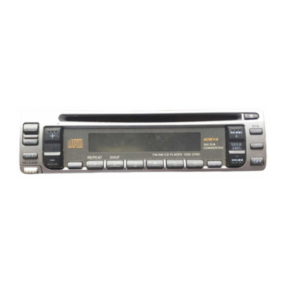
Sony CDX-3700 Service Manual
Fm/am compact disc player
Hide thumbs
Also See for CDX-3700:
- Operating instructions manual (26 pages) ,
- Cautions leaflet (1 page) ,
- Operating instructions (2 pages)
Table of Contents
Advertisement
Quick Links
SERVICE MANUAL
• The tuner and CD sections have no adjustments.
CD player section
System
Compact disc digital audio
system
Signal-to-noise ratio
90 dB
Frequency response
10 – 20,000 Hz
Wow and flutter
Below measurable limit
Tuner section
FM
Tuning range
FM tuning interval:
50 kHz/200 kHz
switchable
87.5 – 108.0 MHz
(at 50 kHz step)
87.5 – 107.9 MHz
(at 200 kHz step)
Aerial terminal
External aerial connector
Intermediate frequency 10.7 MHz
Usable sensitivity
12 dBf
Selectivity
75 dB at 400 kHz
Signal-to-noise ratio
65 dB (stereo),
68 dB (mono)
Harmonic distortion at 1 kHz
0.7% (stereo),
0.5% (mono)
Separation
35 dB at 1 kHz
Frequency response
30 – 15,000 Hz
AM
Tuning range
AM tuning interval:
9 kHz/10 kHz switchable
531 – 1,602 kHz
(at 9 kHz step)
530 – 1,710 kHz
(at 10 kHz step)
Aerial terminal
External aerial connector
Intermediate frequency 10.7 MHz/450 kHz
Sensitivity
30 µV
MICROFILM
CDX-3700
Model Name Using Similar Mechanism
CD Drive Mechanism Type
SPECIFICATIONS
Power amplifier section
Outputs
Speaker impedance
Maximum power output 40 W × 4 (at 4 ohms)
General
Outputs
Tone controls
Power requirements
Dimensions
Mounting dimensions
Mass
Supplied accessories
Design and specifications are subject to change without
notice.
FM/AM COMPACT DISC PLAYER
– 1 –
E Model
Speaker outputs
(sure seal connectors)
4 – 8 ohms
Line output
Power amplifier control
lead
Power aerial relay control
lead
Bass ±8 dB at 100 Hz
Treble ±8 dB at 10 kHz
12 V DC car battery
(negative ground)
Approx. 178 × 50 × 178 mm
(w/h/d)
Approx. 182 × 53 × 162 mm
(w/h/d)
Approx. 1.2 kg
Parts for installation and
connections (1 set)
NEW
MG-310-153
Advertisement
Table of Contents

Related Manuals for Sony CDX-3700


Summary of Contents for Sony CDX-3700
- Page 1 CDX-3700 SERVICE MANUAL E Model • The tuner and CD sections have no adjustments. Model Name Using Similar Mechanism CD Drive Mechanism Type MG-310-153 SPECIFICATIONS CD player section Power amplifier section System Compact disc digital audio Outputs Speaker outputs system...
-
Page 2: Table Of Contents
COMPONENTS IDENTIFIED BY MARK ! OR DOTTED LINE WITH MARK ! ON THE SCHEMATIC DIAGRAMS AND IN THE PARTS LIST ARE CRITICAL TO SAFE OPERATION. REPLACE THESE COMPONENTS WITH SONY PARTS WHOSE PART NUMBERS APPEAR AS SHOWN IN THIS MANUAL OR IN SUPPLEMENTS PUBLISHED BY SONY. - Page 3 SECTION 1 GENERAL This section is extracted from instruction manual. – 3 –...
- Page 4 – 4 –...
- Page 5 – 5 –...
- Page 6 – 6 –...
- Page 7 – 7 –...
-
Page 8: Disassembly
SECTION 2 DISASSEMBLY Note : Follow the disassembly procedure in the numerical order given. 2-1. COVER 1 claw 4 cover 3 claws 2 claw 2-2. FRONT PANEL ASSY 2 front panel assy 1 button (release) – 8 –... -
Page 9: Key Board
2-3. KEY BOARD 1 P 2x10 5 claws 3 claws 2 P 2x10 4 claws 6 claws 7 back panel !™ button (source) 8 KEY board !£ button (+. -) !¢ spring (release) 9 button (6 key) 0 button (AMS) !¡... -
Page 10: Cd Mechanism Block
2-5. CD MECHANISM BLOCK 7 CD mechanism block 1 PTT 2.6x8 3 claw 2 claw 5 CNJ102 6 CN600 4 CNJ103 2-6. HEAT SINK 4 heat sink 3 PTT 2.6x8 2 PTT 2.6x8 1 PTT 2.6x8 – 10 –... -
Page 11: Chassis (R) Block Assy
2-7. CHASSIS (R) BLOCK ASSY 3 tension spring (FL) 4 tension spring (FL) 2 chassis (R) block assy 1 screws (P 2x2.5) 2-8. FLOATING BLOCK ASSY 4 tension spring (SPM) 0 floating block assy 5 tension spring (angle) 3 lever (LE.L) 2 washer (M) 1 tension spring (lever D) –... -
Page 12: Roller Arm Assy
2-9. ROLLER ARM ASSY 1 spring (roller) 7 roller arm assy 2 spring (roller) 2-10. OPTICAL PICK-UP BLOCK 1 gear (worm wheel) 2 shaft (sled guide) 3 optical pick-up block claw – 12 –... -
Page 13: Diagrams
SECTION 3 DIAGRAMS 3-1. IC PIN DESCRIPTION • IC600 µPD780058GC-063-8BT (SYSTEM CONTROL) Pin No. Pin Name Pin Description MCLK Microcomputer command clock signal output (data latch on rising) MDATA Microcomputer command data signal output Microcomputer command load signal output AVSS —... - Page 14 Pin No. Pin Name Pin Description PLLCKO PLL clock output PLLSI PLL data input AMON AM ON output — — Not used in this set. FMST ST-IND indication input/Forced Monaural output Switch 4 input (“L” active) Switch 3 input (“L” active) Switch 1 input (“L”...
-
Page 15: Block Diagram
CDX-3700 3-2. BLOCK DIAGRAM DIGITAL SIGNAL/ ELECTRIC VOLUME RF AMP SERVO PROCESSOR OPTICAL IC400 IC102 IC101 PICK-UP CNP400 R-CH LINE OUT L OUT REAR VOL/ FADER TONE R OUT R-CH Q401 POWER AMP RFENV IC500 CNP500 CROSS TRCRS VDET REAR L(+) -
Page 16: Printed Wiring Boards -Main Section
CDX-3700 3-3. PRINTED WIRING BOARDS — MAIN SECTION — • Semiconductor Location Ref. No. Location (D501) B-10 D503 B-13 D504 B-12 D505 C-11 D506 D-13 D507 D-12 D508 E-11 D509 F-11 D510 E-12 D511 D512 E-10 D513 D514 D516 B-12... - Page 17 CDX-3700 S602 FREQUENCY SELECT FM50k AM9k FM200k AM10k S600 (RESET) (Page 30) – 19 – – 20 –...
-
Page 18: Schematic Diagram -Main Section (1/3)
CDX-3700 3-4. SCHEMATIC DIAGRAM — MAIN SECTION (1/3) — • Refer to page 31 for IC Block Diagrams. • Waveforms (MODE:PLAY) 1.3Vp-p (ARF) IC102 (Page 23) Approx. 200mVp-p @™ (TE) IC102 Approx. 600mVp-p @£ IC102 (FE) Note: • All capacitors are in µF unless otherwise noted. pF: µµF 50 WV or less are not indicated except for electrolytics and tantalums. -
Page 19: Schematic Diagram -Main Section (2/3)
CDX-3700 3-5. SCHEMATIC DIAGRAM — MAIN SECTION (2/3) — • Refer to page 32 for IC Block Diagrams. (Page 26) Note: • All capacitors are in µF unless otherwise noted. pF: µµF 50 WV or less are not indicated except for electrolytics and tantalums. -
Page 20: Schematic Diagram -Main Section (3/3)
CDX-3700 3-6. SCHEMATIC DIAGRAM — MAIN SECTION (3/3) — • Refer to page 32 for IC Block Diagrams. (Page 23) Note: • All capacitors are in µF unless otherwise noted. pF: µµF • Power voltage is dc 14.4V and fed with regulated dc power •... -
Page 21: Schematic Diagram -Display Section
CDX-3700 3-7. SCHEMATIC DIAGRAM — DISPLAY SECTION — (Page 26) Note: • All capacitors are in µF unless otherwise noted. pF: µµF • Power voltage is dc 14.4V and fed with regulated dc power 50 WV or less are not indicated except for electrolytics supply from ACC and BATT cords. -
Page 22: Printed Wiring Board -Display Section
CDX-3700 3-8. PRINTED WIRING BOARD — DISPLAY SECTION — PL802 PL801 D801 (Page 19) Note: • ® : Through hole. • b : Pattern from the side which enables seeing. (The other layer’s patterns are not indicated.) Caution: Pattern face side: Parts on the pattern face side seen from the (Side B) pattern face are indicated. - Page 23 • IC Block Diagrams IC102 AN8835SB F CH VCBA E CH F BAL T BAL A CH VCBA B CH CCRS TE BPF RF DET RF EQ BDO DET CAGC V DET CSBRT OFFR DET OFFR 3 TENV CROSS LD ON NRF DET IC103 BA5984FP-E2 MUTE...
- Page 24 IC400 LC75374E LFIN – LFOUT – – – – LSELO LROUT – – VREF CONTROL – SHIFT – DECODER LATCH REGISTER RROUT RSELO – – – – RFOUT – RFIN 6 7 8 9 10 IC700 TB2118F 24 XI REGULATED POWER SUPPLY 23 A GND REFERENCE...
-
Page 25: Exploded Views
SECTION 4 EXPLODED VIEWS NOTE: • The mechanical parts with no reference • Color Indication of Appearance Parts The components identified by number in the exploded views are not supplied. mark ! or dotted line with mark. Example : • Items marked “*” are not stocked since KNOB, BALANCE (WHITE) ... -
Page 26: Front Panel Section
4-2. FRONT PANEL SECTION not supplied (KEY board) LCD800 Ref. No. Part No. Description Remark Ref. No. Part No. Description Remark 3-035-311-01 PANEL, BACK 3-034-443-01 BUTTON (6 KEY) * 52 3-034-440-01 PLATE (LCD), GROUND 3-034-451-01 BUTTON (AMS) * 53 3-034-454-01 SHEET (LCD) 3-034-445-01 BUTTON (EJECT) * 54 3-034-453-01 SHEET (DIFFUSION) -
Page 27: Cd Mechanism Section (1)
4-3. CD MECHANISM SECTION (1) (MG-310-153) M103 Ref. No. Part No. Description Remark Ref. No. Part No. Description Remark 3-342-940-01 WASHER (M) A-3301-687-A CHASSIS (M) BLOCK ASSY * 102 3-032-327-01 LEVER (LE.L) * 112 1-670-827-11 SW BOARD 3-037-492-01 DAMPER (P) 3-033-807-01 SCREW (M2X3.0) 3-033-808-01 SCREW (M2X4.0) 3-032-359-01 SPRING (ROLLER) -
Page 28: Cd Mechanism Section (2)
4-4. CD MECHANISM SECTION (2) (MG-310-153) M101 not supplied M102 not supplied not supplied The components identified by mark ! or dotted line with mark. ! are critical for safety. Replace only with part number specified. Ref. No. Part No. Description Remark Ref. -
Page 29: Electrical Parts List
SECTION 5 MAIN ELECTRICAL PARTS LIST NOTE: • Due to standardization, replacements in • Items marked “*” are not stocked since The components identified by mark ! or dotted line with mark. the parts list may be different from the they are seldom required for routine service. - Page 30 MAIN Ref. No. Part No. Description Remark Ref. No. Part No. Description Remark < CAPACITOR > C405 1-109-982-11 CERAMIC CHIP C406 1-162-967-11 CERAMIC CHIP 0.0033uF 10% C101 1-117-681-11 ELECT CHIP 100uF C407 1-164-227-11 CERAMIC CHIP 0.022uF C102 1-109-982-11 CERAMIC CHIP C408 1-109-982-11 CERAMIC CHIP C103...
- Page 31 MAIN Ref. No. Part No. Description Remark Ref. No. Part No. Description Remark C517 1-107-826-11 CERAMIC CHIP 0.1uF C745 1-162-911-11 CERAMIC CHIP 0.5PF C519 1-162-915-11 CERAMIC CHIP 10PF 0.5PF C746 1-162-907-11 CERAMIC CHIP 0.25PF 50V C520 1-107-826-11 CERAMIC CHIP 0.1uF C901 1-117-370-11 CERAMIC CHIP 10uF...
- Page 32 MAIN Ref. No. Part No. Description Remark Ref. No. Part No. Description Remark < COIL > R116 1-216-847-11 METAL CHIP 150K 1/16W R117 1-216-839-11 METAL CHIP 1/16W L400 1-412-058-11 INDUCTOR CHIP 10uH R119 1-216-817-11 METAL CHIP 1/16W L501 1-416-729-11 INDUCTOR 420uH R120 1-216-845-11 RES,CHIP...
- Page 33 MAIN Ref. No. Part No. Description Remark Ref. No. Part No. Description Remark R485 1-216-837-11 RES,CHIP 1/16W R630 1-216-821-11 RES,CHIP 1/16W R501 1-218-722-11 METAL CHIP 0.50% 1/16W R701 1-216-833-11 RES,CHIP 1/16W R502 1-216-833-11 RES,CHIP 1/16W R702 1-216-825-11 RES,CHIP 2.2K 1/16W R503 1-218-748-11 METAL CHIP 220K...
- Page 34 CDX-3700 MOTOR Ref. No. Part No. Description Remark Ref. No. Part No. Description Remark 1-670-828-11 MOTOR BOARD PARTS FOR INSTALLATION AND CONNECTIONS ************* *************************************** < SWITCH > 3-009-613-21 FRAME X-3366-405-1 SCREW ASSY (EXP), FITTING 1-762-946-12 SWITCH, PUSH (1 KEY) (LIMIT)