
Related Manuals for LG FLATRON L1810B


Summary of Contents for LG FLATRON L1810B
- Page 1 COLOR MONITOR SERVICE MANUAL CHASSIS NO. : CL-42 FACTORY MODEL: LB800K MODEL: L1810B(LB800K-VL) CAUTION BEFORE SERVICING THE UNIT, READ THE SAFETY PRECAUTIONS IN THIS MANUAL.
-
Page 2: Table Of Contents
CONTENTS SPECIFICATIONS ........... 2 ADJUSTMENT ............12 PRECAUTIONS ............4 TROUBLESHOOTING GUIDE ......13 TIMING CHART ............5 PRINTED CIRCUIT BOARD........18 OPERATING INSTRUCTIONS ........ 6 EXPLODED VIEW...........22 WIRING DIAGRAM ..........8 REPLACEMENT PARTS LIST .......24 BLOCK DIAGRAM ........... 9 PIN CONFIGURATION..........28 DESCRIPTION OF BLOCK DIAGRAM....10 SCHEMATIC DIAGRAM ......... - Page 3 Signal Connector Pin Assignment • DVI-I Connector (Digital/Analog) Signal (DVI-I) Signal (DVI-I) T. M. D. S. Data2- Hot Plug Detect T. M. D. S. Data2+ T. M. D. S. Data0- T. M. D. S. Data2/4 Shield T. M. D. S. Data0+ T.
-
Page 4: Precautions
PRECAUTION WARNING FOR THE SAFETY-RELATED COMPONENT. WARNING BE CAREFUL ELECTRIC SHOCK ! • There are some special components used in LCD monitor that are important for safety. These parts are • If you want to replace with the new backlight (CCFL) or marked on the schematic diagram and the inverter circuit, must disconnect the AC adapter... -
Page 5: Timing Chart
TIMING CHART VIDEO SYNC << Dot Clock (MHz), Horizontal Frequency (kHz), Vertical Frequency (Hz), Horizontal etc... (µs), Vertical etc... (ms) >> Total Period Video Active Time Front Porch Sync Duration Back Porch Sync Mode Resolution Frequency Clock Polarity Sort 31.469 640x350 25.175 70Hz... -
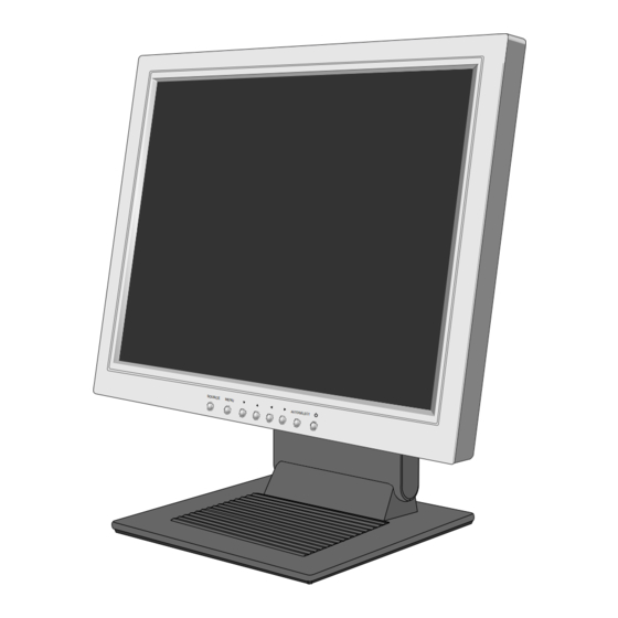
Page 6: Operating Instructions
OPERATING INSTRUCTIONS FRONT VIEW REAR VIEW Power Connect USB Port Front Control Panel D-Sub Signal DVI Connect Connect Front Control Panel 1. Power ON/OFF Button 5. AUTO/SELECT Button Use this button to turn the monitor on or off. Use this button to enter a selection in the On Screen Display. 2. - Page 7 Making use of USB (Universal Serial Bus)* USB (Universal Serial Bus) is an innovation in connecting your different desktop peripherals conveniently to your computer. By using the USB, you will be able to connect your mouse, keyboard, and other to your monitor instead of having to connect them to your computer.
-
Page 8: Wiring Diagram
6631T25008Q Connector Ass’y P/N: Connector Ass’y P/N: 6631T20015R P902 MATAL FRAME J706 J703 Connector Ass’y P/N: J710 J702 6631T12002M Connector Ass’y P/N: 6631T12002L CN1A MODULE Connector Ass’y P/N: 6631T11012P... -
Page 9: Block Diagram
Bus-power USB Inverte r Output LCD Module Inverter R,G,B differential LVDS:Low Voltage Differential Signaling Flash Memory LVDS (LVD S823) Data 8 Bit or 16 Bit Add ress Out - CLK DE ,H/V Sync out R,G,B Even DVDD 3.3V AVD D 3.3V Gm5120 2.5V 3.3V... -
Page 10: Description Of Block Diagram
DESCRIPTION OF BLOCK DIAGRAM 1. Input signal switching part. There are two inputs which are analog and digital input. They come from each 15 pin D-Sub and 24 pin DVI-D connector. 2. Video Controller Part. This part amplifies the level of video signal for the digital conversion and converts from the analog video signal to the digital video signal using a pixelclock. - Page 11 50 ~ 60Hz 100KHz HVDC INPUT RECTIFIER ENERGY OUTPUT RECTIFIER COMPONENTS AND FILTER TRANSFER AND FILTER LINE 100 ~ 240V SIGNAL PWM CONTROL PHOTO-COUPLER COLLENT- CIRCUIT ISOLATION PRIMARY SECONDARY Operation description_Power 1. EMI components. This part contains of EMI components to comply with global marketing EMI standards like FCC, VCCI CISPR, the circuit included a line-filter, across line capacitor and of course the primary protection fuse.
-
Page 12: Adjustment
ADJUSTMENT All adjustment are thoroughly checked and corrected 3. Adjustment for White Balance when the monitor leaves the factory, but sometimes 1) Display color 0,0 pattern at Mode 15. 2) Select COLOR → BIAS CALIBRATION command several minor adjustment may be required. Adjustment should be following procedure and after and Enter. -
Page 13: Troubleshooting Guide
TROUBLESHOOTING GUIDE 1. NO POWER NO POWER (POWER INDICATOR OFF) CHECK J703 TROUBLE IN INPUT VOLTAGE POWER (12V) ? CHECK J703 TROUBLE IN 5VST VOLTAGE POWER (5V) ? CHECK U203’s PIN 151. TROUBLE IN IS THIS PIN U203 or X201 OSCILLATED? TROUBLE SOMEWHERE ELSE... - Page 14 2. NO RASTER NO RASTER CHECK J703 PIN 1, 2 TROUBLE IN (12V) ? POWER CHECK TROUBLE IN J705 PIN 28, 29, 30 POWER (5V) ? CHECK TROUBLE IN U801 U801 (3.3V)? CHECK TROUBLE IN U201 ? U201 CHECK TROUBLE IN R234, R235, R237 U203 PULSE?
- Page 15 CHECK CHECK DOT CLOCK U401 PIN 10 PATTERN PULSE ? CHECK CHECK U401 PIN 8 V.PULSE? DVS PATTERN CHECK CHECK U401 PIN 7 DHS PATTERN H.PULSE? TROUBLE IN LCD MODULE - 15 -...
- Page 16 3. NO CLOCK (CLOCK GENERATOR) NO DOT CLOCK CHECK TROUBLE IN X201 20MHz ? X201 CHECK TROUBLE IN R237 U203 CLOCK ? - 16 -...
- Page 17 4. TROUBLE IN DPM TROUBLE IN DPM CHECK PC CHECK PC IS NOT GOING R711, R712? INTO DPM OFF MODE CHECK U203 PIN 152 TROUBLE IN WAVEFORM X201 (20MHz) ? CHECK TROUBLE IN U203 PIN 44 SIGNAL CABLE TROUBLE IN PC - 17 -...
- Page 19 D711 C231 R702 D718 C224 C225 R732 D717 C222 C233 C216 R726 R727 D720 C221 C242 C728 C223 C226 C220 D719 R237 C241 C213 C727 C284 D722 C240 R236 D721 C239 R235 C230 C283 R282 C212 D724 C238 C219 C229 R234 C218 C209...
- Page 20 3. POWER BOARD (Component Side) 4. POWER BOARD (Solder Side)
- Page 21 5. CONTROL BOARD 6.USB BOARD...
-
Page 23: Exploded View
CABINET ASSEMBLY, LB800K BRAND L039 ABS SILVER SPRAY 3091TKL038J LCD(LIQUID CRYSTAL DISPLAY), LM181E06-A4C3 LG PHILPS TFT COLOR SXGA LVDS SMM 6304FLP044A LCD(LIQUID CRYSTAL DISPLAY), LM181E06-A4M1 LG PHILPS TFT COLOR SXGA 18.1" LVDS SMM or6304FLP034A BACK COVER ASSEMBLY, LB800H L030A 85964 3809TKL025A TILT SWIVEL ASSEMBLY, LB800H . -
Page 24: Replacement Parts List
REPLACEMENT PARTS LIST CAUTION: BEFORE REPLACING ANY OF THESE COMPONENTS, READ CAREFULLY THE SAFETY PRECAUTIONS IN THIS MANUAL. * NOTE SAFETY Mark AL ALTERNATIVE PARTS DATE: 2002. 11. 06. DATE: 2002. 11. 06. *S *AL LOC. NO. PART NO. DESCRIPTION / SPECIFICATION *S *AL LOC. - Page 25 DATE: 2002. 11. 06. DATE: 2002. 11. 06. *S *AL LOC. NO. PART NO. DESCRIPTION / SPECIFICATION *S *AL LOC. NO. PART NO. DESCRIPTION / SPECIFICATION COILs & COREs C817 0CE107WF6DC 100UF MVK 16V 20% R/TP(SMD) C818 0CC102CK41A 1000PF 1608 50V 5% R/TP NP0 L101 6210TCE001G HH-1M3216-501 CERATEC 3216M...
- Page 26 DATE: 2002. 11. 06. DATE: 2002. 11. 06. *S *AL LOC. NO. PART NO. DESCRIPTION / SPECIFICATION *S *AL LOC. NO. PART NO. DESCRIPTION / SPECIFICATION R243 0RJ3302D677 33K OHM 1/10 W 5% 1608 R/TP R767 0RJ0752D677 75 OHM 1/10 W 5% 1608 R/TP R246 0RJ1000D677 100 OHM 1/10 W 5% 1608 R/TP...
- Page 27 DATE: 2002. 11. 06. DATE: 2002. 11. 06. *S *AL LOC. NO. PART NO. DESCRIPTION / SPECIFICATION *S *AL LOC. NO. PART NO. DESCRIPTION / SPECIFICATION C916 181-288L MKT 100V 823JTR PHS26823 LED1 0DLLT0208AA LITEON LTST-C155KGJSKT R/TP C918 0CE228ED630 2200UF KMG,RD 10V 20% BULK USB BOARD C919 0CKZTTA003B...
-
Page 28: Pin Configuration
PIN CONFIGURATION BA7657F BLOCK DIAGRAM Red 1 input HD 1 input HD Sync Signal detector HD 2 input Green 1 input HD output Ground Red output DET. Blue 1 input Ground Green output Composite video input Red 2 input (Sync on Green) Syncsepa Ground Composite sync output... - Page 29 S524A40X10/40X20/40X40 SCL SDA S524A40X10/ 40X20/40X40 NOTE: The S524A40X10/40X20/40X40 is available in 8-pin DIP, SOP, and TSSOP package. Figure 2-2. Pin Assignment Diagram Table 2-1. S524A40X10/40X20/40X40 Pin Descriptions Circuit Name Type Description Type A0, A1, A2 Input Input pins for device address selection. To configure a device address, these pins should be connected to the V or V of the device.
- Page 30 Start/Stop HV Generation Logic Timing Control Control Logic EEPROM Cell Array Slave Address Word Address 128 x 8 bits Comparator Pointer decoder 256 x 8 bits 512 x 8 bits Column Decoder Data Register and ACK Figure 2-1. S524A40X10/40X20/40X40 Block Diagram...