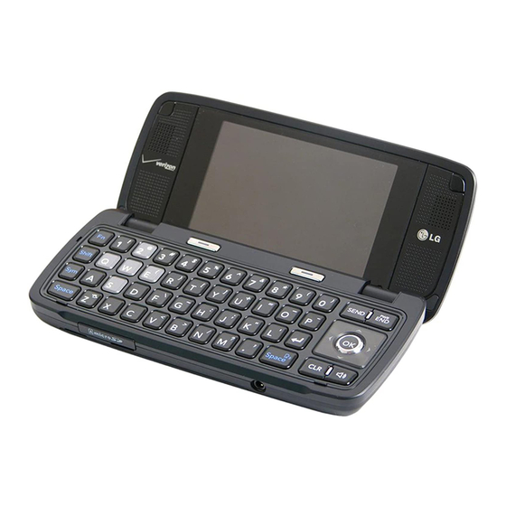
LG VX10000 Service Manual
Dual band cdma [pcs/cellular/gps/media flo] cdma mobile phone
Hide thumbs
Also See for VX10000:
- Hints and tips manual (64 pages) ,
- Datasheet (2 pages) ,
- User manual (354 pages)
Table of Contents
Advertisement
Quick Links
Features of VX10000
1. Wave Type
● CELLULAR : G7W
● PCS: G7W
2. Frequency Scope
Transmit Frequency (MHz)
CELLULAR
824.82 ~ 848.19
3. Rated Output Power : CELLULAR = 0.28W
4. Output Conversion Method : This is possible by correcting the key board channel.
5. Voltage and Current Value of Termination Part Amplifier (Catalogue included)
MODE
CELLULAR
PCS
6. Functions of Major Semi-Conductors
Classification
MSM6550
Memory MCP
(TYA000BC10H0GG)
RFR6500
RFT6150
7. Frequency Stability
● CELLULAR : ±0.5PPM
● PCS : ±0.1PPM
PCS
CELLULAR
1850~1910
869.82~893.19
PCS = 0.28W
Part Name
Voltage
AWT6321R
4.2V
AWT6321R
4.2V
Terminal operation control and digital signal processing
Flash Memory (2Gbit) + SDRAM (1Gbit)
Storing of terminal operation program
Converts Rx RF signal to baseband signal
Converts baseband signal to Tx RF signal
Receive Frequency (MHz)
PCS
1930~1990
Current
Power
400mA
0.28W
400mA
0.28W
Function
GPS
1575.42
Advertisement
Table of Contents
Troubleshooting

Related Manuals for LG VX10000


Summary of Contents for LG VX10000
- Page 1 Features of VX10000 1. Wave Type ● CELLULAR : G7W ● PCS: G7W 2. Frequency Scope Transmit Frequency (MHz) Receive Frequency (MHz) CELLULAR CELLULAR 824.82 ~ 848.19 1850~1910 869.82~893.19 1930~1990 1575.42 3. Rated Output Power : CELLULAR = 0.28W PCS = 0.28W 4.
- Page 2 VX10000 CDMA Mobile Subscriber Unit VX10000 SERVICE MANUAL SERVICE MANUAL DUAL BAND CDMA [PCS/Cellular/GPS/Media FLO] CDMA MOBILE PHONE Copyright © 2007 LG Electronics. Inc. All right reserved LGE Internal Use Only - 1 - Only for training and service purposes...
-
Page 3: Table Of Contents
3.4 Backlight……………………………………………………………………………………..97 3.5 Vibrator……………………………………………………………………………………..99 3.6 Audio………………………………………………………………………………………...101 3.7 Touch Screen………………………………………………………………………………110 CHAPTER 5. Safety ………………………………………………..………………..………133 CHAPTER 6. Glossary ………………….……………………………………………….…136 APPENDIX ………………………………………………………………………………...……148 Copyright © 2007 LG Electronics. Inc. All right reserved LGE Internal Use Only - 2 - Only for training and service purposes... -
Page 4: General Introduction
Cellular uses 800MHz and PCS uses 1.9GHz. The VX10000 support GPS Mode, we usually call it tri-band phone. Also, VX10000 works on Advanced Mobile Phone Service (S-GPS). We call it dual- mode phone. If one of the Cellular, PCS base stations is located nearby, Call fail rate of triple-mode phone is less than dual-mode phone or single-mode phone. -
Page 5: Chapter 1. System Introduction
At this time, the spectrums of other signals that have different codes are not recovered into its original state, and appears as the self-interference of the system. Copyright © 2007 LG Electronics. Inc. All right reserved LGE Internal Use Only... -
Page 6: Features And Advantages Of Cdma Mobile Phone
1.25msec (800 times per second). By doing so, the gain tolerance and the different radio propagation loss on the forward/backward link are complemented. Copyright © 2007 LG Electronics. Inc. All right reserved LGE Internal Use Only... - Page 7 That is, each mobile station signal generates interference in relation to the signals of all the other mobile stations. Copyright © 2007 LG Electronics. Inc. All right reserved LGE Internal Use Only...
- Page 8 Copyright © 2007 LG Electronics. Inc. All right reserved LGE Internal Use Only...
-
Page 9: Structure And Functions Of Dual-Band Cdma Mobile Phone
Transmit signals obtained pass through the duplexer filter and then, are sent out to the cell site via the antenna. Copyright © 2007 LG Electronics. Inc. All right reserved LGE Internal Use Only... -
Page 10: Specification
About 480 Hours (SCI=2) Standby Time About 480 Hours (SCI=2) CELLULAR 150 Minutes (-92dBm input) Talk time 150 Minutes (-92dBm input) Copyright © 2007 LG Electronics. Inc. All right reserved LGE Internal Use Only - 9 - Only for training and service purposes... - Page 11 Single Tone : -30dBm at 900 kHz (CELLULAR), -30dBm at 1.25MHz(PCS) Two Tone : -43dBm at 900 kHz & 1700kHz(CELLULAR), -43dBm at 1.25 MHz & 2.05 MHz (PCS) Copyright © 2007 LG Electronics. Inc. All right reserved LGE Internal Use Only...
- Page 12 1852.50 1872.50 1892.50 1853.75 1873.75 1893.75 1855.00 1875.00 1895.00 1856.25 1876.25 1896.25 1857.50 1877.50 1897.50 1858.75 1878.75 1898.75 Copyright © 2007 LG Electronics. Inc. All right reserved LGE Internal Use Only - 11 - Only for training and service purposes...
- Page 13 1975.00 1936.25 1956.25 1976.25 1937.50 1957.50 1977.50 1938.75 1958.75 1978.75 1940.00 1960.00 1000 1980.00 1941.25 1961.25 1025 1981.25 Copyright © 2007 LG Electronics. Inc. All right reserved LGE Internal Use Only - 12 - Only for training and service purposes...
- Page 14 4.5.4 Bluetooth mode : 2400 MHz ~ 2483.5 MHz 4.6 AC Adaptor : See Appendix 4.7 Cigar Lighter Charger : See Appendix Copyright © 2007 LG Electronics. Inc. All right reserved LGE Internal Use Only - 13 - Only for training and service purposes...
-
Page 15: Installation
Install the microphone either by clipping I onto the sunvisor (driver’s side) or by attaching it to door post (driver’s side), using a velcro adhesive tape (not included). 5.3.5 Cable Connections Copyright © 2007 LG Electronics. Inc. All right reserved LGE Internal Use Only - 14 -... - Page 16 5.3.5.2 Antenna Cable Connection Connect the antenna coupler cable connector from the cradle to the external antenna connector. ( Antenna is not included.) Copyright © 2007 LG Electronics. Inc. All right reserved LGE Internal Use Only - 15 - Only for training and service purposes...
-
Page 17: Chpater 2. Nam Input Method
You can see the MEID/ESN number. Press softkey “OK” (Message key) to edit more NAM1 items. Press softkey “Exit” (Contacts) to exit Service Programming. Copyright © 2007 LG Electronics. Inc. All right reserved LGE Internal Use Only - 16 -... - Page 18 You can edit the NAM1 Home SID. Press softkey “OK” (Message key) to edit more NAM1 items. Press softkey “Back” (Contacts) to edit previous NAM1 items. Copyright © 2007 LG Electronics. Inc. All right reserved LGE Internal Use Only - 17 -...
- Page 19 You can edit Service Code. Press softkey “OK” (Message key) to edit more NAM1 items. Press softkey “Back” (Contacts) to edit previous NAM1 items. Copyright © 2007 LG Electronics. Inc. All right reserved LGE Internal Use Only - 18 -...
- Page 20 You can edit NAM1 True IMSI MCC. Press softkey “OK” (Message key) to edit more NAM1 items. Press softkey “Back” (Contacts) to edit previous NAM1 items. Copyright © 2007 LG Electronics. Inc. All right reserved LGE Internal Use Only - 19 -...
- Page 21 You can edit NAM1 Home SID/NID pair. Press softkey “OK” (Message key) to edit more NAM1 items. Press softkey “Back” (Contacts) to edit previous NAM1 items. Copyright © 2007 LG Electronics. Inc. All right reserved LGE Internal Use Only - 20 -...
- Page 22 You can edit NAM1 CDMA Primary Channel B. Press softkey “OK” (Message key) to edit more NAM1 items. Press softkey “Back” (Contacts) to edit previous NAM1 items. Copyright © 2007 LG Electronics. Inc. All right reserved LGE Internal Use Only - 21 -...
- Page 23 Press softkey “OK” (Message key) to edit more NAM1 items. Press softkey “Back” (Contacts) to edit previous NAM1 items. Press Left, Right, Up, Down key to toggle Yes/No. Copyright © 2007 LG Electronics. Inc. All right reserved LGE Internal Use Only - 22 -...
- Page 24 You can view the NAM1 Access Overload Class. Press softkey “OK” (Message key) to edit more NAM1 items. Press softkey “Back” (Contacts) to edit previous NAM1 items. Copyright © 2007 LG Electronics. Inc. All right reserved LGE Internal Use Only - 23 -...
- Page 25 You can edit Slot Cycle Index. Press softkey “OK” (Message key) to save Slot Cycle Index. Press softkey “Back” (Contacts) to edit previous items. Copyright © 2007 LG Electronics. Inc. All right reserved LGE Internal Use Only - 24 -...
- Page 26 VX10000 28) Powering Down Restart. Copyright © 2007 LG Electronics. Inc. All right reserved LGE Internal Use Only - 25 - Only for training and service purposes...
-
Page 27: Chapter 3. Circuit Description
After that, the RF signal is amplified by the Power Amp in order to have enough power for radiation. Finally, the RF signal is sent out to the cell site via the antenna after going through the duplexer. Copyright © 2007 LG Electronics. Inc. All right reserved LGE Internal Use Only... - Page 28 VX10000 [Figure 1-1] RF Block Diagram of VX10000 Diplexer Copyright © 2007 LG Electronics. Inc. All right reserved LGE Internal Use Only - 27 - Only for training and service purposes...
- Page 29 It’s main function is to limit the bandwidth of spectrum reaching the LNA and mixer, attenuate receiver spurious response and suppress local oscillator energy. As a result frequency sensitivity and selectivity of mobile phone increase. The specification of VX10000 duplexer described below ; PCS duplexer:...
- Page 30 The characteristics of Low Noise Amplifier (LNA) are low noise figure, high gain, high intercept point and high reverse isolation. The frequency selectivity characteristic of mobile phone is mostly determined by LNA. The specification of VX10000 GPS LNA is described below Parameter...
- Page 31 Intercept Point (IIP3) requirements of IS-98D and J-STD-018 specifications for Sensitivity, Two-Tone Inter- modulation, and Single-tone Desensitization. Operation modes and band selection are specially controlled from the Mobile Station Modem MSM6550. The specification of VX10000 Mixers is described below: Parameter Low gain High gain...
- Page 32 R and C filter in order to generate the reference frequency of 19.2 MHz and input it into the frequency synthesizer. Frequency stability depending on temperature is ±2.0 ppm. Copyright © 2007 LG Electronics. Inc. All right reserved LGE Internal Use Only...
-
Page 33: Digital/Voice Processing Part
2.2.5 Power Supply Part The power supply part is made up of circuits for generating various types of power, used for the digital/voice processing part. Copyright © 2007 LG Electronics. Inc. All right reserved LGE Internal Use Only - 32 -... - Page 34 Then, the errors of data received from viterbi decoder are detected and corrected. They are voice-decoded at the vocoder in order to output digital voice data. Copyright © 2007 LG Electronics. Inc. All right reserved LGE Internal Use Only...
- Page 35 VX10000 [Figure 2-2] Block Diagram of Digital/Voice Processing Part Diplexer Copyright © 2007 LG Electronics. Inc. All right reserved LGE Internal Use Only - 34 - Only for training and service purposes...
- Page 36 MSM6550. It is also supplied stable +2.8V_LCD by Out6 in U5002 for wide view angle and LCD reflects to improve the display efficiency. 4 LEDs is used to display LCD backlight. Copyright © 2007 LG Electronics. Inc. All right reserved LGE Internal Use Only...
-
Page 37: Chapter 4. Trouble Shooting
4. Check RF Signal path 2. Check VCTCXO 5. Check Rx I/Q data Redownload S /W , Cal Copyright © 2007 LG Electronics. Inc. All right reserved LGE Internal Use Only - 36 - Only for training and service purposes... - Page 38 VX10000 1.1.1 Checking DC Power supply circuit (PMIC) Test Point Test Point R5014 R5013 Circuit Diagram Circuit Diagram Copyright © 2007 LG Electronics. Inc. All right reserved LGE Internal Use Only - 37 - Only for training and service purposes...
- Page 39 Refer to Logic troubleshoot DC Po wer supply Circuit is OK. See next Page to check VCTCXO circuit Copyright © 2007 LG Electronics. Inc. All right reserved LGE Internal Use Only - 38 - Only for training and service purposes...
- Page 40 VX10000 1.1.2 Checking VCTCXO circuit Test Point Test Point U1010 pin4 U1010 pin3 Circuit Diagram Circuit Diagram Copyright © 2007 LG Electronics. Inc. All right reserved LGE Internal Use Only - 39 - Only for training and service purposes...
- Page 41 Is it similar? to check control signal . Replace Main B /D Waveform Waveform Figure 1.1 (a) Figure 1.1 (b) Copyright © 2007 LG Electronics. Inc. All right reserved LGE Internal Use Only - 40 - Only for training and service purposes...
- Page 42 VX10000 1.1.3 Checking Control signal Test Point Test Point U1011 pin49(SBST0) pin50(SBDT0) pin51(SBCK0) Circuit Diagram Circuit Diagram Copyright © 2007 LG Electronics. Inc. All right reserved LGE Internal Use Only - 41 - Only for training and service purposes...
- Page 43 RF signal path . To Figure 1.1 (c), (d) Replace Main B /D Waveform Waveform Figure 1.1 (c) Figure 1.1 (d) Copyright © 2007 LG Electronics. Inc. All right reserved LGE Internal Use Only - 42 - Only for training and service purposes...
- Page 44 L1026,L1027,C1051 F1001. Pin6 DP1001. Pin3 PCS Tx DCN Tx PCS Rx Circuit Diagram Circuit Diagram DCN Rx RFR6500 Copyright © 2007 LG Electronics. Inc. All right reserved LGE Internal Use Only - 43 - Only for training and service purposes...
- Page 45 Is any signal detected at Check L1026,1027,C1051 that point? RF signal path is OK. See next page to Rx I/Q data signal Copyright © 2007 LG Electronics. Inc. All right reserved LGE Internal Use Only - 44 - Only for training and service purposes...
- Page 46 VX10000 Waveform Waveform U1001 pin2 1.1 (e) F1001 pin6 1.1 (f) DP1001 pin3 1.1 (g) Copyright © 2007 LG Electronics. Inc. All right reserved LGE Internal Use Only - 45 - Only for training and service purposes...
- Page 47 1.1.5 Checking Rx I/Q data Test Point Test Point U1011 Pin7 (RX0_QM) Pin8 (RX0_QP) Pin9 (RX0_IM) Pin10 (RX0_IP) Circuit Diagram Circuit Diagram Copyright © 2007 LG Electronics. Inc. All right reserved LGE Internal Use Only - 46 - Only for training and service purposes...
- Page 48 , change Main B /D . Waveform Waveform RX0_QP RX0_IP RX0_Q RX0_IM RX_Q_ RX_Q_ Graph 1.1(i) Graph 1.1(h) Copyright © 2007 LG Electronics. Inc. All right reserved LGE Internal Use Only - 47 - Only for training and service purposes...
-
Page 49: Pcs Rx
DC Power Supply circuit 4. Check RF Signal path 2. Check VCTCXO 5. Check Rx I/Q data Redownload S/W, Cal Copyright © 2007 LG Electronics. Inc. All right reserved LGE Internal Use Only - 48 - Only for training and service purposes... - Page 50 VX10000 1.2.1 Checking DC Power supply circuit (PMIC) Test Point Test Point R5014 R5013 Circuit Diagram Circuit Diagram Copyright © 2007 LG Electronics. Inc. All right reserved LGE Internal Use Only - 49 - Only for training and service purposes...
- Page 51 Refer to Logic troubleshoot +2.6V_MSMP3 is OK? DC Po wer supply Circuit is OK. See next Page to check VCTCXO circuit Copyright © 2007 LG Electronics. Inc. All right reserved LGE Internal Use Only - 50 - Only for training and service purposes...
- Page 52 VX10000 1.2.2 Checking VCTCXO circuit Test Point Test Point U1010 pin4 U1010 pin3 Circuit Diagram Circuit Diagram Copyright © 2007 LG Electronics. Inc. All right reserved LGE Internal Use Only - 51 - Only for training and service purposes...
- Page 53 Is it similar? to check control signal . Replace Main B /D Waveform Waveform Figure 1.2 (a) Figure 1.2 (b) Copyright © 2007 LG Electronics. Inc. All right reserved LGE Internal Use Only - 52 - Only for training and service purposes...
- Page 54 VX10000 1.2.3 Checking Control signal Test Point Test Point U1011 pin49(SBST0) pin50(SBDT0) pin51(SBCK0) Circuit Diagram Circuit Diagram Copyright © 2007 LG Electronics. Inc. All right reserved LGE Internal Use Only - 53 - Only for training and service purposes...
- Page 55 RF signal path . To Figure 1.2 (c), (d) Replace Main B /D Waveform Waveform Figure 1.2 (c) Figure 1.2 (d) Copyright © 2007 LG Electronics. Inc. All right reserved LGE Internal Use Only - 54 - Only for training and service purposes...
- Page 56 L1017,C1028,C1029, Pin6 L1025 DP1002. Pin2 Circuit Diagram Circuit Diagram PCS Tx DCN Tx PCS Rx DCN Rx RFR6500 Copyright © 2007 LG Electronics. Inc. All right reserved LGE Internal Use Only - 55 - Only for training and service purposes...
- Page 57 Is any signal detected at Check L1017,C1028,C1029,L1025 that point? RF signal path is OK. See next page to Rx I/Q data signal Copyright © 2007 LG Electronics. Inc. All right reserved LGE Internal Use Only - 56 - Only for training and service purposes...
- Page 58 1.2 (e) F1001 Pin 4 1.2 (f) DP1002 Pin 2 Figure 4.1.2 (c) Figure 4.1.2 (c) 1.2 (g) Copyright © 2007 LG Electronics. Inc. All right reserved LGE Internal Use Only - 57 - Only for training and service purposes...
- Page 59 1.2.5 Checking Rx I/Q data Test Point Test Point U1011 Pin7 (RX0_QM) Pin8 (RX0_QP) Pin9 (RX0_IM) Pin10 (RX0_IP) Circuit Diagram Circuit Diagram Copyright © 2007 LG Electronics. Inc. All right reserved LGE Internal Use Only - 58 - Only for training and service purposes...
- Page 60 , change Main B /D . Waveform Waveform RX0_QP RX0_IP RX0_Q RX0_IM RX_Q_ RX_Q_ Graph 1.2(i) Graph 1.2(h) Copyright © 2007 LG Electronics. Inc. All right reserved LGE Internal Use Only - 59 - Only for training and service purposes...
-
Page 61: Tx Part Trouble Shooting
DC Power Supply circuit 7. Check Diplexer 2. Check VCTCXO 8. Check Mobile Switch 3. Check RFT6150 Redownload S/W, Cal Copyright © 2007 LG Electronics. Inc. All right reserved LGE Internal Use Only - 60 - Only for training and service purposes... - Page 62 VX10000 2.1.1 Checking DC Power supply circuit (PMIC) Test Point Test Point C5033 R5013 Circuit Diagram Circuit Diagram Copyright © 2007 LG Electronics. Inc. All right reserved LGE Internal Use Only - 61 - Only for training and service purposes...
- Page 63 Refer to Logic trouble shoot DC Po wer supply Circuit is OK. See next Page to check VCTCXO circuit Copyright © 2007 LG Electronics. Inc. All right reserved LGE Internal Use Only - 62 - Only for training and service purposes...
- Page 64 VX10000 2.1.2 Checking VCTCXO circuit Test Point Test Point U1010 pin4 U1010 pin3 Circuit Diagram Circuit Diagram Copyright © 2007 LG Electronics. Inc. All right reserved LGE Internal Use Only - 63 - Only for training and service purposes...
- Page 65 Is it similar? to check control signal . Replace Main B /D Waveform Waveform Figure 2.1 (a) Figure 2.1 (b) Copyright © 2007 LG Electronics. Inc. All right reserved LGE Internal Use Only - 64 - Only for training and service purposes...
- Page 66 PIN 29 PIN 30 TX_IP PIN 1, 2, 3, 4 TX_IM TX_ON, SBCK0, SBDT0, SBST0 Circuit Diagram Circuit Diagram Copyright © 2007 LG Electronics. Inc. All right reserved LGE Internal Use Only - 65 - Only for training and service purposes...
- Page 67 Check pin2, 3, 4(TP5) at U1012 Check SBI signal line & MSM Referring to Figure 2.1(f). Is it similar? Replace U1012 Copyright © 2007 LG Electronics. Inc. All right reserved LGE Internal Use Only - 66 - Only for training and service purposes...
- Page 68 VX10000 Waveform Waveform Graph 2.1(c) Graph 2.1 (f) RX_I_P RX_Q_P RX_Q_N RX_I_N Graph 2.1(d) Graph 2.1 (e) Copyright © 2007 LG Electronics. Inc. All right reserved LGE Internal Use Only - 67 - Only for training and service purposes...
- Page 69 F 1005 . Referring to Figure 2.1(h) Is it similar ? RF_OUT Replace F 1005 Figure 2.1(g) Copyright © 2007 LG Electronics. Inc. All right reserved LGE Internal Use Only - 68 - Only for training and service purposes...
- Page 70 Test Point Test Point RFOUT_CELL VCCA DCN Tx VBATT PCS Tx VEN_CELL RFIN_CELL VMODE Circuit Diagram Circuit Diagram Copyright © 2007 LG Electronics. Inc. All right reserved LGE Internal Use Only - 69 - Only for training and service purposes...
- Page 71 Waveform Waveform RF_IN fed up with CW signal in low gain mode of PAM RF_IN RF_OUT Figure 2.1(i) Copyright © 2007 LG Electronics. Inc. All right reserved LGE Internal Use Only - 70 - Only for training and service purposes...
- Page 72 DP 1001 . Referring to Figure 2.1(j) Is it similar ? Replace DP 1001 ANT Port Figure 2.1(j) Copyright © 2007 LG Electronics. Inc. All right reserved LGE Internal Use Only - 71 - Only for training and service purposes...
- Page 73 Diplexer is at F1001 . Referring to Figure 2.1(k) Is it similar ? Replace F1001 ANT Port Figure 2.1(k) Copyright © 2007 LG Electronics. Inc. All right reserved LGE Internal Use Only - 72 - Only for training and service purposes...
- Page 74 Mobile S/W is at U1001 . Referring to Figure 2.1(l) Is it similar ? Replace U1001 RF OUT Figure 2.1(l) Copyright © 2007 LG Electronics. Inc. All right reserved LGE Internal Use Only - 73 - Only for training and service purposes...
-
Page 75: Pcs Tx
DC Power Supply circuit 7. Check Diplexer 2. Check VCTCXO 8. Check Mobile Switch 3. Check RFT6150 Redownload S/W, Cal Copyright © 2007 LG Electronics. Inc. All right reserved LGE Internal Use Only - 74 - Only for training and service purposes... - Page 76 VX10000 2.2.1 Checking DC Power supply circuit (PMIC) Test Point Test Point C5033 R5013 Circuit Diagram Circuit Diagram Copyright © 2007 LG Electronics. Inc. All right reserved LGE Internal Use Only - 75 - Only for training and service purposes...
- Page 77 Refer to Logic trouble s hoot DC Po wer supply Circuit is OK. See next Page to check VCTCXO circuit Copyright © 2007 LG Electronics. Inc. All right reserved LGE Internal Use Only - 76 - Only for training and service purposes...
- Page 78 VX10000 2.2.2 Checking VCTCXO circuit Test Point Test Point U1010 pin4 U1010 pin3 Circuit Diagram Circuit Diagram Copyright © 2007 LG Electronics. Inc. All right reserved LGE Internal Use Only - 77 - Only for training and service purposes...
- Page 79 Is it similar? to check control signal . Replace Main B /D Waveform Waveform Figure 2.2 (a) Figure 2.2 (b) Copyright © 2007 LG Electronics. Inc. All right reserved LGE Internal Use Only - 78 - Only for training and service purposes...
- Page 80 PIN 29 PIN 30 TX_IP PIN 1, 2, 3, 4 TX_IM TX_ON, SBCK0, SBDT0, SBST0 Circuit Diagram Circuit Diagram Copyright © 2007 LG Electronics. Inc. All right reserved LGE Internal Use Only - 79 - Only for training and service purposes...
- Page 81 Check pin2, 3, 4(TP5) at U1012 Check SBI signal line & MSM Referring to Figure 2.2(f). Is it similar? Replace U1012 Copyright © 2007 LG Electronics. Inc. All right reserved LGE Internal Use Only - 80 - Only for training and service purposes...
- Page 82 Waveform Waveform Figure 2.2(c) Figure 2.2(e) RX_I_P RX_Q_P RX_Q_N RX_I_N Figure 2.2(d) SBDT SBST SBCK SBCK Figure 2.2(f) Copyright © 2007 LG Electronics. Inc. All right reserved LGE Internal Use Only - 81 - Only for training and service purposes...
- Page 83 RF Tx SAW is at F 1006 . Referring to Figure 2.2(h) Is it similar? RF_OUT Replace F 1005 Figure2.2(h) Copyright © 2007 LG Electronics. Inc. All right reserved LGE Internal Use Only - 82 - Only for training and service purposes...
- Page 84 2.2.5 Check PCS PAM circuit Test Point Test Point RFOUT_PCS VEN_PCS VMODE VBATT RFIN_PCS Circuit Diagram Circuit Diagram DCN Tx PCS Tx Copyright © 2007 LG Electronics. Inc. All right reserved LGE Internal Use Only - 83 - Only for training and service purposes...
- Page 85 Replace U1008 Waveform Waveform RF_IN fed up with CW signal in low gain mode of PAM RF_OUT Figure 2.2(i) Copyright © 2007 LG Electronics. Inc. All right reserved LGE Internal Use Only - 84 - Only for training and service purposes...
- Page 86 DP 1002 . Referring to Figure 2.2(j) Is it similar ? Replace DP 1002 ANT Port Figure 2.2(j) Copyright © 2007 LG Electronics. Inc. All right reserved LGE Internal Use Only - 85 - Only for training and service purposes...
- Page 87 Diplexer is at F1001 . Referring to Figure 2.2(k) Is it similar ? Replace F1001 ANT Port Figure 2.2(k) Copyright © 2007 LG Electronics. Inc. All right reserved LGE Internal Use Only - 86 - Only for training and service purposes...
- Page 88 Mobile S/W is at U1001 . Referring to Figure 2.1(l) Is it similar ? Replace U1001 RF OUT Figure 2.2(l) Copyright © 2007 LG Electronics. Inc. All right reserved LGE Internal Use Only - 87 - Only for training and service purposes...
-
Page 89: Logic Part Trouble Shooting
R5020 +2.8V_TCXO R5013 +2.6V_MSMP3 +2.85V_RX R5014 Test point Test point +1.8V_MSMP1 +2.85V_RX +2.8V_TCXO +1.4V_MSMC +2.8V_TCXO U5002 +2.6V_MSMP3 +2.6V_MSMA Copyright © 2007 LG Electronics. Inc. All right reserved LGE Internal Use Only - 88 - Only for training and service purposes... - Page 90 Does it work properly ? Re-download software and try again Re-download software and try again The Phone will power on Copyright © 2007 LG Electronics. Inc. All right reserved LGE Internal Use Only - 89 - Only for training and service purposes...
- Page 91 Circuit Diagram Test point Test point Q5002 Q5005 Pin1 CON 5001 CON6004 +5V_CHAR of U5001 +5V_USB_char of U5001 Copyright © 2007 LG Electronics. Inc. All right reserved LGE Internal Use Only - 90 - Only for training and service purposes...
- Page 92 The battery may have the problem. Is the battery charged? Change the battery and try again. Charging will operate properly Copyright © 2007 LG Electronics. Inc. All right reserved LGE Internal Use Only - 91 - Only for training and service purposes...
-
Page 93: Lcd
MLCD_CS/, SLCD_CS/,M_IM0, M_IM1,S_IM0,S_IM1, WE2/ Test point Test point CON6001 F6012 F6006 F6007 F6011 +2.8V_LCD(R5011) F6013 U5002 F6009 F6010 Copyright © 2007 LG Electronics. Inc. All right reserved LGE Internal Use Only - 92 - Only for training and service purposes... - Page 94 Check the control signal D2[0:15], Check : F6006,F6007,F6009,F6010,F6011 RESET/,LCD_CS/,WE/,IM0,IM1 F6012, F6013 (Signal line) Check CON6001solder ing Re-solderCON6001 LCD display will work properly Copyright © 2007 LG Electronics. Inc. All right reserved LGE Internal Use Only - 93 - Only for training and service purposes...
-
Page 95: Camera
C5043 +2.8V_CAM_VDD C5048 +1.8V_CAM_VDD C5047 +2.8V_CAM_AVDD • Camera Control signals From MSM : CAM_DATA[0:7], CAM_REST/, CAM_SDA, CAM_SCL, CAM_CLK_IN, CAM_PCLK Copyright © 2007 LG Electronics. Inc. All right reserved LGE Internal Use Only - 94 - Only for training and service purposes... - Page 96 - The Soldering of connector CON6003 F6002 R6006 F6005 U3006 F6004 L3003 F6003 C5043 C5048 C5047 U5004 U5005 Copyright © 2007 LG Electronics. Inc. All right reserved LGE Internal Use Only - 95 - Only for training and service purposes...
- Page 97 CAM_DATA[0:7], CAM_RESET/, Check the F6002, F6003,F6004,F6005(Signal line) CAM_SDA, CAM_SCL Check CON6003 Soldering Re-solder CON6003 Camera will work properly Copyright © 2007 LG Electronics. Inc. All right reserved LGE Internal Use Only - 96 - Only for training and service purposes...
-
Page 98: Backlight
Circuit Diagram Circuit Diagram LED100 side LED101 side LED101 side lighting lighting lighting Test point Test point Q600 Copyright © 2007 LG Electronics. Inc. All right reserved LGE Internal Use Only - 97 - Only for training and service purposes... - Page 99 Check the soldering of each R and LEDs, Are all LEDs working ? Or replace if not working Main key backlight will work properly Copyright © 2007 LG Electronics. Inc. All right reserved LGE Internal Use Only - 98 - Only for training and service purposes...
-
Page 100: Vibrator
VX10000 3.5 Vibrator Circuit Diagram Circuit Diagram C3104 3.0V_LIN_MOTOR Test point Test point U3101 U3100 U3102 C3104 U3103 Copyright © 2007 LG Electronics. Inc. All right reserved LGE Internal Use Only - 99 - Only for training and service purposes... - Page 101 Replace the U3100,U3101 Check the state at contact of vibrator Re-contact vibrator Replace Vibrator The vibrator will Work properly Copyright © 2007 LG Electronics. Inc. All right reserved LGE Internal Use Only - 100 - Only for training and service purposes...
-
Page 102: Audio
3.6 Audio 3.6.1 Speaker Trouble Circuit Diagram Circuit Diagram Test point Test point C4003 U4002 C4018(DNI) C4006 C4007 C4017(DNI) Copyright © 2007 LG Electronics. Inc. All right reserved LGE Internal Use Only - 101 - Only for training and service purposes... - Page 103 Replace U4002 C4017,4018 C4017,4018 Re-solder U4002 Check the state Replace Speaker Of contact of speaker Speaker will work properly Copyright © 2007 LG Electronics. Inc. All right reserved LGE Internal Use Only - 102 - Only for training and service purposes...
- Page 104 VX10000 3.6.2 Receiver Trouble Circuit Diagram Circuit Diagram MSM6550 Test point Test point R2103 R2104 Copyright © 2007 LG Electronics. Inc. All right reserved LGE Internal Use Only - 103 - Only for training and service purposes...
- Page 105 Replace MSM R2104,R2103 R2104,R2103 Re-solder R2104,2103 Check the state Replace Receiver Of contact of receiver Receiver will work properly Copyright © 2007 LG Electronics. Inc. All right reserved LGE Internal Use Only - 104 - Only for training and service purposes...
- Page 106 Circuit Diagram Circuit Diagram Test point Test point Pin 3 (EAR_L) CON4001 Pin 2 (EAR_R) R4022 R4021 U4003 Copyright © 2007 LG Electronics. Inc. All right reserved LGE Internal Use Only - 105 - Only for training and service purposes...
- Page 107 1.2V ? Check soldering of Re-soldering of Pin2,3 of CON4001 Pin2,3 of CON4001 Change main board Copyright © 2007 LG Electronics. Inc. All right reserved LGE Internal Use Only - 106 - Only for training and service purposes...
- Page 108 Level of pin4 of CON4001 Re-solder Is 1.65~2.10V? R4021 Does it work? Download SW Change main Does it work well? board Copyright © 2007 LG Electronics. Inc. All right reserved LGE Internal Use Only - 107 - Only for training and service purposes...
- Page 109 VX10000 3.6.4 Mic Trouble Circuit Diagram Circuit Diagram Test point Test point R2014 M2000 Copyright © 2007 LG Electronics. Inc. All right reserved LGE Internal Use Only - 108 - Only for training and service purposes...
- Page 110 C2004, C2008 C2004, C2008 Check the soldering of Re-solder MIC NETWORK MIC NETWORK MIC will work properly Copyright © 2007 LG Electronics. Inc. All right reserved LGE Internal Use Only - 109 - Only for training and service purposes...
-
Page 111: Touch Screen
Circuit Diagram 3.7.1 Touch Trouble Connector Touch IC Test point Test point C6033 TOUCH_PENIRQ C6032 TOUCH_SCL C6031 TOUCH_SDA Copyright © 2007 LG Electronics. Inc. All right reserved LGE Internal Use Only - 110 - Only for training and service purposes... - Page 112 Does SDA and SCL come out as shown in picture? Problem Calibrate Touch Window will work properly Graph 3.7(a) Copyright © 2007 LG Electronics. Inc. All right reserved LGE Internal Use Only - 111 - Only for training and service purposes...
-
Page 113: Chapter 5. Safety
If so, use only a manufacture approves antenna. Otherwise, take your phone to a qualifies service center for repair. Use only the supplied or approved antenna. Non-approved antennas, modifications, or attachments, could impair call quality, damage the phone, and violate FCC regulations. Copyright © 2007 LG Electronics. Inc. All right reserved LGE Internal Use Only - 112 -... - Page 114 Copyright © 2007 LG Electronics. Inc. All right reserved LGE Internal Use Only - 113 -...
- Page 115 Rule of Thumb: Using common sense at all times when handling, installing or using the phone. Any questions should be directed to you nearest Service Center or authorized service technician or electrician. Copyright © 2007 LG Electronics. Inc. All right reserved LGE Internal Use Only...
-
Page 116: Chapter 6. Glossary
A-key. A secret, 64-bit pattern stored in the mobile station. It is used to generate update the mobile station’s Shared Secret Data. The A-key is used in the mobile station authentication process. Copyright © 2007 LG Electronics. Inc. All right reserved LGE Internal Use Only... - Page 117 CDMA Channel. The set of channels transmitted between the base station within a given CDMA frequency assignment. See also Forward CDMA Channel and Reverse CDMA Channel. Copyright © 2007 LG Electronics. Inc. All right reserved LGE Internal Use Only - 116 -...
- Page 118 Dim-and-Burst. A frame in which primary traffic is multiplexed with either secondary traffic or signaling traffic. Copyright © 2007 LG Electronics. Inc. All right reserved LGE Internal Use Only...
- Page 119 Paging Channels, and up to 63 Traffic Channels, as long as the total number of channels, including the Pilot Channel, is no greater than 64. Copyright © 2007 LG Electronics. Inc. All right reserved LGE Internal Use Only - 118 -...
- Page 120 Layer 3. Layer 3 provides the control of the Cellular telephone systems. Signaling messages originate and terminate at layer 3. See also Layering and Layer 2. Copyright © 2007 LG Electronics. Inc. All right reserved LGE Internal Use Only - 119 -...
- Page 121 Mobile Switching Center (MSC). A configuration of equipment that provides Cellular radiotelephone service. Also called the Mobile Telephone Switching Office (MTSO) Copyright © 2007 LG Electronics. Inc. All right reserved LGE Internal Use Only - 120 - Only for training and service purposes...
- Page 122 Optional Field. A field defined within a message structure that is optionally to the message recipient. Order. A type of message that contains control codes for either the mobile station or the base station. Copyright © 2007 LG Electronics. Inc. All right reserved LGE Internal Use Only...
- Page 123 Pilot PN Sequence Offset Index. The PN offset in units of 64 PN chips of a pilot, relative to the zero offset pilot PN sequence. Copyright © 2007 LG Electronics. Inc. All right reserved LGE Internal Use Only - 122 -...
- Page 124 Request. A layer 3 message generated by either the mobile station or the base station to retrieve information, ask for service, or command an action. Copyright © 2007 LG Electronics. Inc. All right reserved LGE Internal Use Only - 123 -...
- Page 125 Slotted Mode. An operation mode of the mobile station in which the mobile station monitors only selected slots on the Paging Channel when in the Mobile Station Idle State. Copyright © 2007 LG Electronics. Inc. All right reserved LGE Internal Use Only...
- Page 126 The counter is incremented an average of once per 80 ms period. Time Reference. A reference established by the mobile station that is synchronous with the earliest arriving multipath component used for demodulation. Copyright © 2007 LG Electronics. Inc. All right reserved LGE Internal Use Only - 125 -...
- Page 127 Zone-Based Registration. An autonomous registration method in which the mobile station registers whenever it enters a zone that is not in the mobile station’s zone list. ㎲. Microsecond Copyright © 2007 LG Electronics. Inc. All right reserved LGE Internal Use Only - 126 -...
- Page 128 VX10000 Appendix Appendix Assembly and Disassembly diagram Block and Circuit diagram Part List Component Layout BGA Pin Map Copyright © 2007 LG Electronics. Inc. All right reserved LGE Internal Use Only - 127 - Only for training and service purposes...
- Page 129 1. Assembly and Disassembly Diagram...
- Page 132 2. Block and Circuit Diagram...
- Page 133 VX10000 BLOCK DIAGRAM Check Circuit MAX9775 18pin Temp MSM Core EBI1 (Audio Amp) 512MBit PCB Rev. JTAG I/F SDRAM RFT6150 RF Front End Ear Jack(4Pole) 32bit ARM926EJS Stereo Headset EBI2 with Jazelle Input 1GBit BB to RF Dual QWERTY Backlight...
- Page 134 VX10000 Circuit Diagram ( Main/FPCB )
- Page 135 Main Board Circuit...
- Page 136 Internal Use Only CDMA ANT DCN ANT DCN TX DCN RX PCS ANT PCS TX PCS RX...
- Page 137 Internal Use Only...
- Page 138 Internal Use Only...
- Page 139 Internal Use Only...
- Page 140 Internal Use Only...
- Page 141 Internal Use Only...
- Page 142 Internal Use Only...
- Page 143 FPCB Circuit...
- Page 144 Internal Use Only...
- Page 145 3. Part List...
- Page 146 Main PCB Component List Ref No. Part No. Value Part Name Part Decription MLAZ00 LABEL MLAZ0038301 PID Label 4 Array LG-VX6000 C7012 CAP,CHIP,MAKER ECCH0000104 3 pF,50V,C,NP0,TC,1005,R/TP MCH155A030C C1035 CAP,CHIP,MAKER ECCH0000105 4 pF,50V,C,NP0,TC,1005,R/TP MCH155A040C C1054 CAP,CHIP,MAKER ECCH0000105 4 pF,50V,C,NP0,TC,1005,R/TP MCH155A040C C1055...
- Page 147 Ref No. Part Decription Part No. Value Part Name C1101 CAP,CHIP,MAKER ECCH0000155 10 nF,16V,K,X7R,HD,1005,R/TP MCH153CN103KK C2003 CAP,CHIP,MAKER ECCH0000155 10 nF,16V,K,X7R,HD,1005,R/TP MCH153CN103KK C2017 CAP,CHIP,MAKER ECCH0000155 10 nF,16V,K,X7R,HD,1005,R/TP MCH153CN103KK C2018 CAP,CHIP,MAKER ECCH0000155 10 nF,16V,K,X7R,HD,1005,R/TP MCH153CN103KK C2019 CAP,CHIP,MAKER ECCH0000155 10 nF,16V,K,X7R,HD,1005,R/TP MCH153CN103KK C2020 CAP,CHIP,MAKER ECCH0000155 10 nF,16V,K,X7R,HD,1005,R/TP...
- Page 148 Ref No. Part Decription Part No. Value Part Name C5201 CAP,CHIP,MAKER ECCH0005604 10 uF,6.3V ,M ,X5R ,TC ,1608 ,R/TP GRM188R60J106ME47D C3014 CAP,CHIP,MAKER ECCH0006201 4.7 uF,6.3V ,K ,X5R ,TC ,1608 ,R/TP C1608X5R0J475KT C5003 CAP,CHIP,MAKER ECCH0006201 4.7 uF,6.3V ,K ,X5R ,TC ,1608 ,R/TP C1608X5R0J475KT C5024 CAP,CHIP,MAKER...
-
Page 149: Appendix
Ref No. Part Decription Part No. Value Part Name C1051 CAP,CHIP,MAKER ECZH0000841 56 pF,50V ,J ,NP0 ,TC ,1005 ,R/TP C1005C0G1H560JT C1016 CAP,CHIP,MAKER ECZH0000844 68 pF,50V ,J ,NP0 ,TC ,1005 ,R/TP C1005C0G1H680JT C1017 CAP,CHIP,MAKER ECZH0000844 68 pF,50V ,J ,NP0 ,TC ,1005 ,R/TP C1005C0G1H680JT C1040 CAP,CHIP,MAKER... - Page 150 Ref No. Part Decription Part No. Value Part Name C3013 CAP,CHIP,MAKER ECZH0003103 0.1 uF,10V ,K ,X7R ,HD ,1005 ,R/TP GRM36X7R104K10PT C3021 CAP,CHIP,MAKER ECZH0003103 0.1 uF,10V ,K ,X7R ,HD ,1005 ,R/TP GRM36X7R104K10PT C3100 CAP,CHIP,MAKER ECZH0003103 0.1 uF,10V ,K ,X7R ,HD ,1005 ,R/TP GRM36X7R104K10PT C4001 CAP,CHIP,MAKER...
- Page 151 Ref No. Part Decription Part No. Value Part Name L1015 INDUCTOR,CHIP ELCH0005014 5.6 nH,S ,1005 ,R/TP , HK10055N6S L1019 INDUCTOR,CHIP ELCH0005813 27 nH,J ,1005 ,R/TP , CIH05T27NJNC L1025 INDUCTOR,CHIP ELCH0005813 27 nH,J ,1005 ,R/TP , CIH05T27NJNC L1028 INDUCTOR,CHIP ELCH0005824 82 nH,J ,1005 ,R/TP , CIH05T82NJNC L1035 INDUCTOR,CHIP...
- Page 152 Ref No. Part Decription Part No. Value Part Name R1005 RES,CHIP,MAKER ERHZ0000291 49.9 ohm,1/16W ,F ,1005 ,R/TP MCR01MZSF49R9 R1009 RES,CHIP,MAKER ERHZ0000291 49.9 ohm,1/16W ,F ,1005 ,R/TP MCR01MZSF49R9 R1020 RES,CHIP,MAKER ERHZ0000299 5600 ohm,1/16W ,F ,1005 ,R/TP MCR01MZSF5601 R6018 RES,CHIP,MAKER ERHZ0000315 75 Kohm,1/16W ,F ,1005 ,R/TP MCR01MZSF7502 R1032 RES,CHIP,MAKER...
- Page 153 Ref No. Part Decription Part No. Value Part Name R2020 RES,CHIP,MAKER ERHZ0000494 510 Kohm,1/16W ,J ,1005 ,R/TP MCR01MZSJ514 R7006 RES,CHIP,MAKER ERHZ0000499 5600 ohm,1/16W ,J ,1005 ,R/TP MCR01MZSJ562 R6029 RES,CHIP,MAKER ERHZ0000501 620 ohm,1/16W ,J ,1005 ,R/TP MCR01MZSJ621 R6011 RES,CHIP,MAKER ERHZ0000507 68 Kohm,1/16W ,J ,1005 ,R/TP MCR01MZSJ683 R1012 RES,CHIP,MAKER...
- Page 154 Ref No. Part Decription Part No. Value Part Name L3004 BEAD-INDUCTOR SFBH0000903 600 ohm,1005 , HB-1M1005-601JT F6002 EMI-FILTER SFEY0011401 SMD ,SMD, 18V, 4ch, EMI_ESD Filter (100 Ohm, 7.5pF) ICVE10184E070R101FR F6003 EMI-FILTER SFEY0011401 SMD ,SMD, 18V, 4ch, EMI_ESD Filter (100 Ohm, 7.5pF) ICVE10184E070R101FR F6004 EMI-FILTER...
- Page 155 FPCB Component List Ref No. Part Decription Part No. Value Part Name C100 CAP,CHIP,MAKER ECZH0000813 100 pF,50V ,J ,NP0 ,TC ,1005 ,R/TP C1005C0G1H101JT C101 CAP,CHIP,MAKER ECZH0000813 100 pF,50V ,J ,NP0 ,TC ,1005 ,R/TP C1005C0G1H101JT C102 CAP,CHIP,MAKER ECZH0000813 100 pF,50V ,J ,NP0 ,TC ,1005 ,R/TP C1005C0G1H101JT C104 CAP,CHIP,MAKER...
- Page 156 4. Components Layout...
- Page 159 CON101 CON103 R107...
- Page 161 5. BGA Pin Map...
- Page 162 1. U2004 MSM6550-V5 USED NOT USED PIN #A1 Corner BOTTOM VIEW...
- Page 163 2. U3001 MCP(TYA000BC10H0GG) PIN #A1 Corner USED NOT USED BOTTOM VIEW...
- Page 164 3. U4002 Audio Amp (MAX9775EBX) PIN #A1 Corner USED NOT USED BOTTOM VIEW...