Table of Contents
Advertisement
Please refer to the original service manual for:
CD Mechanism Unit (BRS12C) , Order No. PSG1303059AE
Speaker system SB-AKX100PNK, Order No. PSG1608002CE
TABLE OF CONTENTS
1 Safety Precautions----------------------------------------------- 3
1.1. General Guidelines---------------------------------------- 3
1.2. Before Repair and Adjustment ------------------------- 4
1.3. Protection Circuitry ---------------------------------------- 4
1.4. Safety Parts Information --------------------------------- 5
2 Warning -------------------------------------------------------------- 6
to Electrostatically Sensitive (ES) Devices---------- 6
2.2. Precaution of Laser Diode------------------------------- 6
(PbF)---------------------------------------------------------- 7
2.4. Handling Precautions for Traverse Unit-------------- 7
prevention --------------------------------------------------- 8
3 Service Navigation ----------------------------------------------- 9
3.1. Service Information --------------------------------------- 9
PAGE
SA-AKX100PN
Model No.
SA-AKX100PR
SA-AKX100PS
Product Color: (K)...Black Type
4 Specifications ---------------------------------------------------- 10
5 Location of Controls and Components------------------ 11
5.1. Remote Control Key Button Operation ------------- 11
5.2. Main Unit Key Button Operation---------------------- 12
6 Service Mode ----------------------------------------------------- 13
6.1. Cold-Start -------------------------------------------------- 13
6.2. Sales Demonstration Lock Function ---------------- 13
6.3. Doctor Mode Table--------------------------------------- 14
6.4. Self-Diagnostic Mode ----------------------------------- 16
6.5. Self-Diagnostic Error Code Table -------------------- 16
7 Troubleshooting Guide --------------------------------------- 18
7.1. No Power or No Display-------------------------------- 18
7.2. Bluetooth® Pairing Failure----------------------------- 18
7.3. No Key Function------------------------------------------ 18
7.4. No Remote Control Function-------------------------- 19
7.5. USB Device Cannot Detect---------------------------- 19
© Panasonic Corporation 2016. All rights reserved.
Unauthorized copying and distribution is a violation
of law.
PSG1608001CE
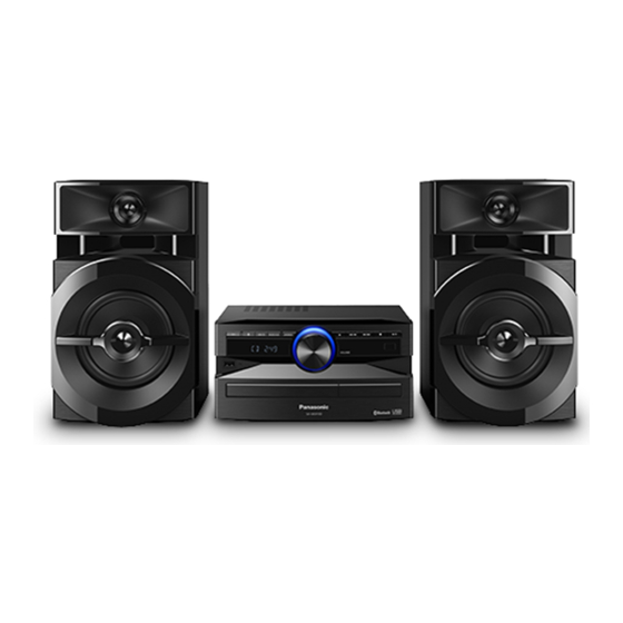
CD Stereo System
PAGE
Advertisement
Table of Contents

Related Manuals for Panasonic SA-AKX100PN


Summary of Contents for Panasonic SA-AKX100PN
-
Page 1: Table Of Contents
7.3. No Key Function------------------------------------------ 18 3 Service Navigation ----------------------------------------------- 9 7.4. No Remote Control Function-------------------------- 19 3.1. Service Information --------------------------------------- 9 7.5. USB Device Cannot Detect---------------------------- 19 © Panasonic Corporation 2016. All rights reserved. Unauthorized copying and distribution is a violation of law. - Page 2 7.6. No Output Sound----------------------------------------- 19 7.7. Check Point------------------------------------------------ 20 8 Disassembly and Assembly Instructions --------------- 21 8.1. Types of Screws ------------------------------------------ 21 8.2. Disassembly Flow Chart-------------------------------- 22 8.3. Main Components and P.C.B. Locations ----------- 22 8.4. Disassembly of Top Cabinet--------------------------- 23 8.5.
-
Page 3: Safety Precautions
1 Safety Precautions 1.1. General Guidelines 1. IMPORTANT SAFETY NOTICE There are special components used in this equipment which are important for safety. These parts are marked by in the Schematic Diagrams, Circuit Board Layout, Exploded Views and Replacement Parts List. It is essential that these critical parts should be replaced with manufacturer’s specified parts to prevent X-RADIATION, shock, fire, or other hazards. -
Page 4: Before Repair And Adjustment
1.2. Before Repair and Adjustment Disconnect AC power to discharge AC capacitor (in SMPS Module) as indicate below diagram through a 10 Ω, 10 W resistor to ground. Caution: DO NOT SHORT-CIRCUIT DIRECTLY (with a screwdriver blade, for instance), as this may destroy solid state devices. After repairs are completed, restore power gradually using a variac to avoid overcurrent. -
Page 5: Safety Parts Information
1.4. Safety Parts Information Safety Parts List: There are special components used in this equipment which are important for safety. These parts are marked by in the Schematic Diagrams, Exploded View & Replacement Parts List. It is essential that these critical parts should be replaced with manufacturer’s specified parts to prevent shock, fire or other hazards. -
Page 6: Warning
2 Warning 2.1. Prevention of Electrostatic Discharge (ESD) to Electrostatically Sensi- tive (ES) Devices Some semiconductor (solid state) devices can be damaged easily by static electricity. Such components commonly are called Elec- trostatically Sensitive (ES) Devices. The following techniques should be used to help reduce the incidence of component damage caused by electrostatic discharge (ESD). -
Page 7: General Description About Lead Free Solder (Pbf)
Figure 2-1 2.3. General description about Lead Free Solder (PbF) The lead free solder has been used in the mounting process of all electrical components on the printed circuit boards used for this equipment in considering the globally environmental conservation. The normal solder is the alloy of tin (Sn) and lead (Pb). -
Page 8: Grounding For Electrostatic Breakdown Prevention
ble cable, cut off the antistatic FFC. Figure 2-2 2.5. Grounding for electrostatic breakdown prevention • As for parts that use optical pick-up (laser diode), the optical pick-up is destroyed by the static electricity of the working environ- ment. Repair in the working environment that is grounded. 2.5.1. -
Page 9: Service Navigation
3 Service Navigation 3.1. Service Information This service manual contains technical information which will allow service personnel’s to understand and service this model. Please place orders using the parts list and not the drawing reference numbers. If the circuit is changed or modified, this information will be followed by supplement service manual to be filed with original service manual. -
Page 10: Specifications
87.50 MHz to 108.00 MHz analyzer. (50 kHz step) (for PN) 87.5 MHz to 108.0 MHz System: SC-AKX100PN (100 kHz step) (for PR/PS) Main Unit: SA-AKX100PN 87.9 MHz to 107.9 MHz Speakers: SB-AKX100PN (200 kHz step) (for PR/PS) 75 Ω (unbalanced) Antenna terminals... -
Page 11: Location Of Controls And Components
5 Location of Controls and Components 5.1. Remote Control Key Button Operation... -
Page 12: Main Unit Key Button Operation
5.2. Main Unit Key Button Operation... -
Page 13: Service Mode
6 Service Mode Remote control with numeric button (Example: N2QAYB001019 (AKX220)) 6.1. Cold-Start Item Key Operation FL Display Mode Name Description Front Key Cold Start To carry out cold-start or initialize 1. Unplug AC power cord. to shipping mode 2. Press & hold [POWER] button. -
Page 14: Doctor Mode Table
6.3. Doctor Mode Table 6.3.1. Doctor Mode Table 1 Item Key Operation FL Display Mode Name Description Front Key Doctor Mode 1. Press [ ] button on main unit follow by [4] and [7] on remote control. 2. To exit, press [DELETE] button on remote control or, press [POWER, /I] button on Main Unit... - Page 15 6.3.2. Doctor Mode Table 2 Item Key Operation FL Display Mode Name Description Front Key Volume Setting To check the volume setting of the In Doctor Mode: Check main unit. 1. Press [7], [8], [9] button on the remote control. 2.
-
Page 16: Self-Diagnostic Mode
6.4. Self-Diagnostic Mode Key Operation Item FL Display Mode Name Description Front Key Self Diagnostic To enter into self diagnostic checking Step 1: Select CD mode Mode (Ensure no disc is inserted). Step 2: Press & hold [g] button follow by [y/i] on main unit for 2 seconds. - Page 17 6.5.2. CD Mechanism Error Code Table Item Key Operation Solution FL Display (PCB exchange repair) Mode Name Description Front Key Error Code Diagnosis Contents: Press [ ] on main unit Check following: CD H15 CD Open Abnormal for next error. 1.
-
Page 18: Troubleshooting Guide
7 Troubleshooting Guide 7.1. No Power or No Display Press Power Button 1. AC Cord Plug-out Check Secondary Cap. (C5) No Display on Check Primary E-Cap (C1) of Unit or Remote 2. Check Fuse(F1) = 0 ohm or Secondary Rect. Diode (D2) FL Display Measured 300V or more Control... -
Page 19: No Remote Control Function
7.4. No Remote Control Function Press Remote Control Press the Power Button If Cannot FL Display Press Remote All Remote Control No Problem Power Button Power ON of the Unit Show "HELLO" Control Buttons Buttons are Working Found to Power ON the unit (No Display) to Turn ON the Set Check Regulator IC... -
Page 20: Check Point
7.7. Check Point Power PCB Sec. Cap. C5 Fuse (F1) (14V or 33V) Pri. Cap (C1) (0 ohm) (300V or more) Main PCB IC1004_Pin 3 IC1004_Pin 3 1.6V 1.6V C1052 7V/12V IC2501 Pin #1 IC1005_Pin 2 3.3V CN2501_Pin1-3 5V/3.3/12V... -
Page 21: Disassembly And Assembly Instructions
8 Disassembly and Assembly Instructions Caution Note: • This section describes the disassembly and/or assembly procedures for all major printed circuit boards & main compo- nents for the unit. (You may refer to the section of “Main components and P.C.B Locations” as described in the service manual) •... -
Page 22: Disassembly Flow Chart
8.2. Disassembly Flow Chart Top Cabinet Front Panel Unit SMPS Module Main P.C.B. Panel P.C.B. Rear Cabinet CD Mechanism Unit CD Interface P.C.B. 8.3. Main Components and P.C.B. Locations... -
Page 23: Disassembly Of Top Cabinet
8.4. Disassembly of Top Cabinet Step 5 Lift up to remove Top Cabinet. Step 1 Remove 2 screws. Step 2 Remove 2 screws. 8.5. Disassembly of Front Panel Unit • Refer to “Disassembly of Top Cabinet”. Step 1 Detach 17P FFC at connector (CN2501) on Main P.C.B.. -
Page 24: Disassembly Of Panel P.c.b
Step 2 Release tabs at bottom of unit. 8.6. Disassembly of Panel P.C.B. • Refer to “Disassembly of Top Cabinet”. • Refer to “Disassembly of Front Panel Unit”. Step 1 Remove Volume Knob. Step 2 Remove 5 screws. Step 3 Release catches. Step 4 Lift up to remove Panel P.C.B.. -
Page 25: Disassembly Of Main P.c.b
8.7. Disassembly of Main P.C.B. Step 5 Remove 2 screws. Step 6 Remove Main P.C.B.. • Refer to “Disassembly of Top Cabinet”. • Refer to “Disassembly of Front Panel Unit”. Step 1 Remove 4 screws. Step 2 Detach 9P Wire at connector (CON2) on SMPS Module. Step 3 Detach 10P FFC at connector (P2004) on Main P.C.B.. -
Page 26: Disassembly Of Rear Cabinet
Step 2 Detach 9P Wire at connector (CON2) on SMPS Module. Step 2 Remove screw. Step 3 Remove 2 screws. Step 3 Remove Inner Chassis. Step 4 Remove SMPS Module. Step 4 Release catches. Step 5 Remove Rear Cabinet. 8.9. Disassembly of Rear Cabinet •... -
Page 27: Disassembly Of Cd Mechanism Unit
8.10. Disassembly of CD Mecha- Step 4 Lift up Rear Cabinet, Main P.C.B. and Inner Chassis as diagram shown. nism Unit • Refer to “Disassembly of Top Cabinet”. • Refer to “Disassembly of Front Panel Unit”. • Refer to “Disassembly of SMPS Module”. Step 1 Detach 10P FFC at connector (P2004) on Main P.C.B.. -
Page 28: Disassembly Of Cd Interface P.c.b
8.11. Disassembly of CD Interface P.C.B. • Refer to “Disassembly of Top Cabinet”. • Refer to “Disassembly of Front Panel Unit”. • Refer to “Disassembly of SMPS Module”. • Refer to “Disassembly of CD Mechanism Unit”. Step 1 Remove 2 screws. Step 2 Desolder pins of the motor (M7301). -
Page 29: Service Position
9 Service Position Note: Refer to Section 8 for disassembly instruction for the related parts. 9.1. Checking of Panel P.C.B. and Main P.C.B. Step 1 Remove Top Cabinet. Step 2 Remove Front Panel Unit. Step 3 Remove Panel P.C.B.. Step 4 Place Panel P.C.B. on the insulated material as shown. Step 5 Attach 17P FFC at connector (CN2501) on Main P.C.B.. -
Page 31: Block Diagram
MODULE HOST_WAKEUP HOST_WAKE JK6400 UART_TX BT_UART_RX 1 5V BLUETOOTH FREQUENCY USB PORT UART_RX BT_UART_TX DEVICE USB_D- 2 D- (REC/PLAY) BT_CTS BT_UART_RTS USB_D+ 3 D+ LDO_ON BT_WAKE NOTE: “ * ” REF IS FOR INDICATION ONLY SA-AKX100PN/PR/PS SYSTEM CONTROL BLOCK DIAGRAM... -
Page 32: Audio
TUN_RST BST_D TUN_WCK DCLK TUN_BCK JK51 Q6001,Q6002, Q6007,Q6300 DC DETECT TO SYSTEM CONTROL DC DET AMP FAN FM ANT SCLK DSP_SCL 2 FMI CIRCUIT SDIO DSP_SDA SDIN2 VALID /RESET /OTW /FAULT 41 XI X6500 42 XO SA-AKX100PN/PR/PS AUDIO BLOCK DIAGRAM... -
Page 33: Power Supply
PW SOC 1R5V +1.5V VOUT MV-DET CN1002 MV-DET +3.3V IC7001 MV DET +5V VOLTAGE D1014 MV DET REGULATOR SMPS ID FROM/TO SMPS ID SYSTEM PROTECT PW BT 5V PROTECT CONTROL VOUT BT PCONT BT PCONT BT PCONT SA-AKX100PN/PR/PS POWER SUPPLY BLOCK DIAGRAM... -
Page 34: Wiring Connection Diagram
11 Wiring Connection Diagram P2005 TO OPTICAL PICKUP UNIT (CD MECHANISM UNIT) P2004 CN1002 MAIN P.C.B. TO SMPS MODULE CD INTERFACE P.C.B. CN7002 CN2501 CN6001 PANEL P.C.B. SA-AKX100PN/PR/PS WIRING CONNECTION DIAGRAM... -
Page 35: Schematic Diagram
12 Schematic Diagram 12.1. Schematic Diagram Notes • This schematic diagram may be modified at any time with the development of new technology. Notes: S6200: Power switch ( S6201: Open/Close switch ( ). S6202: Stop ( ) switch. S6211: Jukebox switch. S6212: Bluetooth/-Pairing switch. -
Page 37: Main (Micon) Circuit (1/2)
DA: MAIN (DAMP): SCHEMATIC DIAGRAM - 5 LB6404 VR: MAIN (VOLTAGE REGULATOR): SCHEMATIC DIAGRAM - 6 J0JHC0000118 IC2501 PW_SYS_3R3V C0DBZYY00716 USB_D- USB SWITCH USB_OVC USB_PCONT USB PORT (REC/PLAY) USB_D+ R6402 C6404 PW_5V 470K VOUT C2506 C2507 LB6401 J0JHC0000118 SA-AKX100PN/PR/PS MAIN (MICON) CIRCUIT... -
Page 38: Main (Micon) Circuit (2/2)
AU: MAIN (AUX TUNER): SCHEMATIC DIAGRAM - 3 C2143 R2499 DS: MAIN (DSP): SCHEMATIC DIAGRAM - 4 0.22 2.2K BT: MAIN (BLUETOOTH): SCHEMATIC DIAGRAM - 4 DA: MAIN (DAMP): SCHEMATIC DIAGRAM - 5 VR: MAIN (VOLTAGE REGULATOR): SCHEMATIC DIAGRAM - 6 SA-AKX100PN/PR/PS MAIN (MICON) CIRCUIT... -
Page 39: Main (Aux Tuner) Circuit
MI: MAIN (MICON): SCHEMATIC DIAGRAM - 1 ~ 2 DS: MAIN (DSP): SCHEMATIC DIAGRAM - 4 BT: MAIN (BLUETOOTH): SCHEMATIC DIAGRAM - 4 DA: MAIN (DAMP): SCHEMATIC DIAGRAM - 5 VR: MAIN (VOLTAGE REGULATOR): SCHEMATIC DIAGRAM - 6 SA-AKX100PN/PR/PS MAIN (AUX TUNER) CIRCUIT... -
Page 40: Main (Dsp), Main (Bluetooth) And Cd Interface Circuit
RESET_SW MAIN (MICON) DGND CIRCUIT (P2004) OPEN_SW IN SCHEMATIC LDM- DIAGRAM - 1 S7201 LDM+ RESET TRV- TRV+ M7301* TRAVERSE MOTOR NOTE: “ * ” REF IS FOR INDICATION ONLY SA-AKX100PN/PR/PS MAIN (DSP) / MAIN (BLUETOOTH) / CD INTERFACE CIRCUIT... -
Page 41: Main (Damp) Circuit
R6054 SPEAKER PROTECTION C6068 6.8K SWITCH AU: MAIN (AUX TUNER): SCHEMATIC DIAGRAM - 3 DS: MAIN (DSP): SCHEMATIC DIAGRAM - 4 BT: MAIN (BLUETOOTH): SCHEMATIC DIAGRAM - 4 VR: MAIN (VOLTAGE REGULATOR): SCHEMATIC DIAGRAM - 6 SA-AKX100PN/PR/PS MAIN (DAMP) CIRCUIT... -
Page 42: Main (Voltage Regulator) Circuit
MI: MAIN (MICON): SCHEMATIC DIAGRAM - 1 ~ 2 16V220 AU: MAIN (AUX TUNER): SCHEMATIC DIAGRAM - 3 DS: MAIN (DSP): SCHEMATIC DIAGRAM - 4 R1018 BT: MAIN (BLUETOOTH): SCHEMATIC DIAGRAM - 4 DA: MAIN (DAMP): SCHEMATIC DIAGRAM - 5 SA-AKX100PN/PR/PS MAIN (VOLTAGE REGULATOR) CIRCUIT... -
Page 43: Panel Circuit
PW_SYS3R3V R6815 Q6801 R6817 PW_12V Q6802 2.7K PW_12V B1ABCF000176 B1ADCE000012 PW_3R3V PW_3R3V SWITCH Q6804 SWITCH PW_+5V PW_+5V B1ABCF000176 C6803 SWITCH C6802 R6806 C6805 P_GND PW_12V LB6803 J0JHC0000118 PW_+5V LB6805 J0JHC0000118 R6823 D6104 B3AEA0000203 QR6005 B1GBCFGN0018 LED DRIVE SA-AKX100PN/PR/PS PANEL CIRCUIT... -
Page 44: Printed Circuit Board
C1049 R6011 C6025 Q6300 LB2558 R1015 C6500 C6592 C6064 LB2556 C1045 R6067 C6068 C1023 R2580 Q6001 LB2029 R6132 C1026 Q1000 LB2027 Q6007 R1062 R1060 R6056 L6005 C1033 CN1002 Q6002 R1038 (TO SMPS P.C.B.) C1032 PbF 6289-1 6289-1 SA-AKX100PN/PR/PS MAIN P.C.B. -
Page 45: Panel, Cd Interface P.c.b
SENSOR VOLUME CD INTERFACE P.C.B. (REP4945B) M7302* (SPINDLE MOTOR) S7201 (RESET) CN7002 CN7001 M7301* TO LOADING P.C.B. (TRAVERSE (CD MECHANISM MOTOR) UNIT BRS11C) 3556A 3556A NOTE: " * " REF IS FOR INDICATION ONLY SA-AKX100PN/PR/PS PANEL / CD INTERFACE P.C.B. -
Page 47: Voltage And Waveform Measurement
14 Voltage and Waveform Measurement 14.1. Voltage Measurement Note: • Indication Voltage Values are in standard values for the unit measured by the DC electronic circuit tester (high-impedance) with the chassis taken as standard. Therefore, there may exist some errors in voltage values, depending on the internal impedance of the DC circuit tester. •... - Page 48 14.1.2. Main P.C.B. (2/3) REF NO. IC2001 MODE CD PLAY STANDBY REF NO. IC2001 MODE CD PLAY STANDBY REF NO. IC2004 MODE CD PLAY STANDBY REF NO. IC2004 MODE CD PLAY STANDBY REF NO. IC2005 MODE POWER ON IC2501 REF NO. MODE USB A ON IC6000...
- Page 49 14.1.3. Main P.C.B. (3/3) QR1008 REF NO. MODE POWER ON AKX100PN/PR/PS MAIN P.C.B. 14.1.4. Panel P.C.B. QR6005 REF NO. MODE CD PLAY STANDBY AKX100PN/PR/PS PANEL P.C.B.
-
Page 51: Exploded View And Replacement Parts List
15 Exploded View and Replacement Parts List 15.1. Cabinet Parts Location 1 11(FOR PR & PS ONLY) *HEATSINK JK51 JK6002 P2005 P2004 JK6000 *(FIRECONE P.C.B.) (MAIN P.C.B.) 10 (FOR PN ONLY) CN1002 10 (FOR PR & PS ONLY) JK6400 CN2501 (PANEL P.C.B.) VR9000 CN6001... -
Page 52: Packaging
15.2. Packaging (FOR PN ONLY) ACCESSORIES BAG (FOR PS ONLY) REMOTE CONTROL (FOR PR ONLY) SA-AKX100 A3 OI BOOK FM INDOOR ANTENNA SB-AKX100 F R O N T POLYFOAM (LEFT) POLYFOAM (RIGHT) SC-AKX100 PACKAGING DRAWING... -
Page 53: Mechanical Replacement Part List
15.3. Mechanical Replacement Part List Safety Ref. Part No. Part Name & Qty Remarks Description Safety Ref. Part No. Part Name & Qty Remarks RMZX1022-1 PCB SPACER Description RKAX0042-K LEG CUSHION RHD26046-L SCREW CABINET XTB3+10JFJ-J SCREW CHASSIS RHD30007-K2J SCREW RHD26078 SCREW REE1730 RHD30111-31... - Page 54 Safety Ref. Part No. Part Name & Qty Remarks Description RSAX0002 INDOOR ANTENNA...
-
Page 55: Electrical Replacement Parts List
15.4. Electrical Replacement Parts List Safety Ref. Part No. Part Name & Qty Remarks Description Safety Ref. Part No. Part Name & Qty Remarks TRANSISTORS Description Q1000 B1AAJC000019 TRANSISTOR PRINTED CIRCUIT Q1008 B1ADCE000012 TRANSISTOR BOARDS Q1011 MTM761230LBF TRANSISTOR Q2001 B1ADCF000001 TRANSISTOR PCB1 TNPA6289... - Page 56 Safety Ref. Part No. Part Name & Qty Remarks Safety Ref. Part No. Part Name & Qty Remarks Description Description X6500 H0J245500110 OSCILLATOR VARIABLE RESIS- TORS JACKS VR9000 K9AA024Y0012 VOLUME JOG JK51 K4ZZ01000276 CONNECTOR JK6000 K4AC04B00030 JK SPEAKER ESD SUPRESSOR JK6002 K2HA2YYA0009 JK6400...
- Page 57 Safety Ref. Part No. Part Name & Qty Remarks Safety Ref. Part No. Part Name & Qty Remarks Description Description R1026 D0GB104JA065 100K 1/10W R2156 D0GB101JA065 1/10W R1027 D1BB1002A074 1/10W R2157 D0GB122JA065 1.2K 1/10W R1028 D1BB9101A074 9.1K 1/10W R2158 D0GB102JA065 1/10W R1030 D0GB103JA065...
- Page 58 Safety Ref. Part No. Part Name & Qty Remarks Safety Ref. Part No. Part Name & Qty Remarks Description Description R6512 D0GB101JA065 1/10W C1055 F1H1H104B047 0.1uF R6513 D0GB101JA065 1/10W C1056 F1J1A106A043 10uF R6514 D0GB101JA065 1/10W C1058 F1H1H104B047 0.1uF R6520 D0GB470JA065 1/10W C1059 F1H1H104B047...
- Page 59 Safety Ref. Part No. Part Name & Qty Remarks Description C6009 F0A1H105A095 C6018 F1H1H104B047 0.1uF C6019 F1H1H104B047 0.1uF C6020 F1H1E105A153 C6021 F1H1H104B047 0.1uF C6022 F1H1E105A153 C6023 F1H1E105A153 C6024 F1H1H333A954 0.033uF 50V C6025 F1H1H333A954 0.033uF 50V C6027 F1H1H104B047 0.1uF C6028 F1H1H333A954 0.033uF 50V C6030 F1H1H333A954...