Table of Contents
Advertisement
Quick Links
Advertisement
Table of Contents

Related Manuals for Ten-Tec RX-340


Summary of Contents for Ten-Tec RX-340
- Page 1 TECHNICAL MANUAL OPERATION, MAINTENANCE, INSTALLATION INSTRUCTIONS AND ILLUSTRATED PARTS BREAKDOWN HF DSP RECEIVER MODEL RX-340 TEN-TEC, INC. 1185 DOLLY PARTON PARKWAY SEVIERVILLE, TN 37862 THIS MANUAL WAS PREPARED IN ACCORDANCE WITH MIL-HDBK- 1221...
- Page 2 TEN-TEC RX340 AUX/AUDIO OUTPUT PINS Wiring for 15 pin male D type plug; Pin 1 - Ground Pin 2 - Mono audio output (AC coupled audio. Decoupled through a pair of back to back 33 µf capacitors). Pin 3 - Audio line output B...
- Page 3 RECORD OF CHANGES CHANGE DATE TITLE OR BRIEF DESCRIPTION ENTERED BY...
- Page 4 WARNING HIGH VOLTAGE is used in the operation of this equipment. DEATH ON CONTACT may result if personnel fail to observe safety precautions. Learn the areas containing high voltage within the equipment. Be careful not to contact high voltage connections when installing, operating or maintaining this equipment.
-
Page 5: Table Of Contents
TABLE OF CONTENTS PARAGRAPH PAGE LIST OF ILLUSTRATIONS LIST OF TABLES INTRODUCTION viii 1. GENERAL INFORMATION 1-1 PURPOSE AND FUNCTION 1-2 SPECIFICATIONS 1-3 ENVIRONMENTAL CONDITIONS 1-4 MECHANICAL 1-10 1-5 EQUIPMENT/PARTS SUPPLIED 1-11 2. PREPARATION FOR USE AND INSTALLATION 2-1 UNPACKING AND INSPECTION 2-2 MOUNTING 2-3 POWER 2-4 ANTENNA... -
Page 6: Paragraph Page
TABLE OF CONTENTS continued PARAGRAPH PAGE 3. GENERAL THEORY OF OPERATION continued 10 MHz REFERENCE OSCILLATOR (81772) 3-10 DSP/CPU (81807) 3-11 FRONT PANEL CPU (81819) 3-10 3-12 KEYPAD BOARD (81820) 3-11 3-13 LOGIC BOARD ↔ CPU INTERCONNECTIONS 3-11 4. LOCAL OPERATION INTRODUCTION FRONT PANEL OVERVIEW MAIN TUNING KNOB... - Page 7 6. MAINTENANCE INSTRUCTIONS INTRODUCTION CLEANING AND LUBRICATION TROUBLESHOOTING INSPECTION PERFORMANCE VERIFICATION TEST FOR MODEL RX- 6-5.1 TEST EQUIPMENT REQUIRED FOR MODEL RX-340 6-5.2 FUNCTIONAL TESTS FOR MODEL RX-340 7. PREPARATION FOR SHIPMENT OR STORAGE PREPARATION FOR RESHIPMENT PREPARATION FOR STORAGE...
- Page 8 TABLE OF CONTENTS continued PARAGRAPH PAGE 8. SINGLE SOURCE PARTS LIST INTRODUCTION 9. FINAL ASSEMBLY MODEL RX-340 INTRODUCTION 10. ILLUSTRATIONS AND PARTS LIST 10-1 INTRODUCTION 10-1...
-
Page 9: List Of Illustrations
LIST OF ILLUSTRATIONS FIGURE PAGE RX-340 FRONT VIEW RX-340 REAR VIEW RX-340 TOP VIEW RX-340 FRONT PANEL REAR VIEW RX-340 BOTTOM VIEW RX-340 INTERCONNECT DIAGRAM CONNECTION DIAGRAM CONFIGURATION DIAGRAM 5-15 SERIAL/PARALLEL INTERFACE 5-16 DB-25 PIN ASSIGNMENTS 5-17 10-1 MODEL RX-340 BLOCK DIAGRAM... - Page 10 LIST OF ILLUSTRATIONS continued FIGURE PAGE 10-29 81772 TCXO SYNTHESIZER SCHEMATIC 10-38 10-30 81824 POWER SUPPLY FILTER TOP CIRCUIT TRACE 10-42 10-31 81824 POWER SUPPLY FILTER BOTTOM CIRCUIT TRACE 10-43 10-32 81824 POWER SUPPLY FILTER COMPONENT LAYOUT 10-44 10-33 81824 POWER SUPPLY FILTER SCHEMATIC 10-45 10-34 81807 DSP/CPU TOP CIRCUIT TRACE...
- Page 11 LIST OF TABLES TABLE PAGE MODEL RX-340 SINGLE SOURCE PARTS LIST PART MANUFACTURER’S INFORMATION RX-340 MODULES FINAL ASSEMBLY REPLACEABLE PARTS 10-1 81878 RX PRESELECTOR PARTS LIST 10-11 10-2 81823 1 MIXER PARTS LIST 10-18 10-3 81817 2 MIXER/IF PARTS LIST...
-
Page 12: Introduction
INTRODUCTION This technical manual provides operation and maintenance instructions for the RX-340 HF DSP Receiver. The manual was prepared in accordance with MIL-HDBK- 1221, “Department of Defense Handbook for Evaluation of Commercial Off-The-Shelf (COTS) Manuals.” It is organized into ten chapters along with a Table of Contents, List of Illustrations, and List of Tables. -
Page 13: General Information
The RX-340 may be controlled locally from the front panel, or operated remotely through a RS-232 interface. Knobs, switches, and displays are arranged ergonomically into four intuitive control groups. Frequency, Mode, and Tuning Rate are presented in 12.5mm blue-green fluorescent characters on the receiver’s main alphanumeric display. - Page 14 IF monitoring points. A standard DB-25 jack accepts a Multi- drop RS-232 line for remote receiver operation. The RX-340’s built-in power supply is designed for international use, accepting a wide range of voltages and line frequencies.
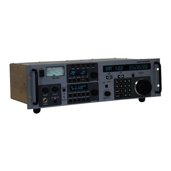
- Page 15 RX-340 FRONT VIEW FIGURE 1-1...
- Page 16 RX-340 REAR VIEW FIGURE 1-2...
-
Page 17: Specifications
1-2 SPECIFICATIONS: Applicable from 50 kHz to 30 MHz, unless otherwise stated. Power Supply: Internal, accepts 48-440 Hz line power, 90-264 VAC. 30 watts nominal. Frequency Tuning System: Tuning Range: 50 kHz to 30 MHz at typical sensitivity. Tunable to 0 MHz with degraded performance. - Page 18 Function: Upper and Lower sideband audio on separate lines in ISB mode. Same signal on both lines in other modes. Single-ended Line-level Audio Outputs: Level: 10 mW into 600 ohms, one AC- coupled and one DC coupled. Connector: DA-15, two pins each-line. Function: Upper, lower, or both sidebands in ISB mode, software configured.
- Page 19 Receiver Sensitivity: Dynamic Range: Noise Figure (dB) 3rd Order Intercept (dBm) Mode 10 dB PREAMP ON PREAMP OFF 15 dB ATTEN VLF Sens.,Typ, .3kHz bandwidth preamp OFF. 16 dB SINAD >500 kHz -116 dBm (.35 µV) 100 kHz -115 dBm (.4 µV) 50 kHz -114 dBm (.45 µV) 20 kHz...
- Page 20 Sensitivity By Mode Preamp OFF Preamp ON Mode SINAD Typical Typical AM: (50% Mod 103 dBm/ -101 dBm/ -112 dBm/ -108 dBm/ 6 kHz 10 dB @ 400Hz) 1.6 µV 2.0 µV 0.56 µV 0.9 µV FM: ( 6kHz dev @ -102 dBm/ -100 dBm/ -108 dBm/...
-
Page 21: Environmental Conditions
Signal Handling Characteristics (Preamp Off): Image Rejection: 90 dB typical, 80 dB minimum (all mixers). IF Rejection: 90 dB typical, 80 dB minimum (all IFs). Third order intercept point: 30 dBm typical, 25 dBm minimum (See chart P1-5). Second order intercept point: +75 dBm, typ, 60 dBm minimum. Selectivity: 57 bandwidths selectable from 0.1 to 16 kHz. -
Page 22: Mechanical
Cooling: Air convection cooled within fan ventilated rack cabinet. Units are directly stackable with no fillers required between chassis. Mounting: Model RX-340 conforms to ETA standard 19” rack mount panel space and is 3U high. Slide mechanism attachment points (10-32 thread) are compatible with Jonathan slide type 375 QD. -
Page 23: Equipment/Parts Supplied
.050 ALLEN WRENCH 38040 .062 ALLEN WRENCH 38088 WARRANTY CARD 74020 RUBBER FEET 42020 LOCK WASHERS 51001 6 x 32 SCREWS 60010 FUSE, 1A, GDC-1A 27071 5 x 20 mm. (spare fuse in power entry module at rear of RX-340). 1-11... - Page 24 This Page Intentionally Left Blank. 1-12...
-
Page 25: Preparation For Use And Installation
Do not attempt to operate the unit if internal damage is noted. 2-2 MOUNTING: RX-340 is designed for ETA standard 19” panel space rack. Slide- mechanism attachment points (10-32 thread) are compatible with Jonathan slide type 375QD. -
Page 26: Line A
2-11 LINE A: An independent 600Ω balanced line-level output is available at DB-15 jack J8. 2-12 LINE B: A second independent-channel 600Ω balanced line-level output is provided at J8. 2-13 AUDIO: A combined-channel 600Ω unbalanced AC-coupled output is provided at 2-14 DC-COUPLED AUDIO: A combined-channel 600 Ω... -
Page 27: General Theory Of Operation
CHAPTER 3 GENERAL THEORY OF OPERATION 3-1 INTRODUCTION: The TEN-TEC Model RX-340 receiver combines a high, dynamic range front end with a versatile DSP back end to provide extraordinary performance and flexibility. Refer to the overall block diagram Figure (10-1) and interconnect diagram Figure (3-4). - Page 28 RX-340 TOP VIEW POWER SUPPLY DSP/CPU 81807 MIXER PRESELECTOR FILTER 81823.SMD 81878 81824 FIGURE 3-1...
- Page 29 RX-340 FRONT PANEL REAR VIEW FRONT PANEL CPU 81819 KEYPAD 81819 (UNDER FRONT PANEL CPU) FIGURE 3-2...
- Page 30 RX-340 BOTTOM VIEW SYNTHESIZER I/0 CONVERTER MIXER POWER SUPPLY 81772.TXCXO 81790.JMD 8187.SMD 21200 FIGURE 3-3...
- Page 31 INTERCONNECT DIAGRAM FIGURE 3-4...
-
Page 32: First Mixer (81823)
3-4 FIRST MIXER (81823): Refer to figure (10-13). Signals from the preselector board are routed through a 30-MHz low-pass filter (L7-L10) and sent to the RF-input port of high-level balanced mixer D1-D4 (T3). The 1st-LO signal is amplified by Q1 and routed through a low-bandpass filter (L5, L6) for application to the mixer’s LO port (T2). -
Page 33: Converter I/O Board (81790)
For receive frequencies above 20 kHz, the PLL is fixed-programmed by the CPU for a reference frequency of 66-2/3 kHz and a VCO frequency of 37-11/15 MHz. 3-6 CONVERTER I/O BOARD (81790): The main A/D and D/A converters on this board provide interface to: (1.) the Digital Signal Processor,... -
Page 34: First Lo Synthesizer (81772)
Controlled by SB select lines from connector 18, U15y and U15z connect either one or both audio channels to the monaural audio driver U18a and to audio connectors 7, 10 and 34, rear panel J8, CPU/ DSP board and front panel mono level control and front-panel phones jack J6. - Page 35 3-10 DSP/CPU (81807): Refer to Figure (10-2). The DSP/CPU board contains two separate processor systems; the MAIN CPU (U1) which controls the RX-340 interface, and the DSP CPU (U15) which performs signal-processing functions. The two systems’ busses integrate through an I/O expansion IC (U11). Communication between the MAIN CPU and the DSP CPU is handled by a combination of hardware and software, providing bi-directional data capability.
- Page 36 second mixer board compares the control voltage to the received signal level and provides feedback to the DSP via connector J73. The two signals on J73 tell the DSP if the applied AGC voltage is greater than or less than an AGC voltage derived from the received signal.
- Page 37 The manual gain port is mounted on the keypad board and the wiper connection returns to the CPU board on connector 85. 3-13 LOGIC BOARD ↔ CPU INTERCONNECTIONS: The RX-340 main logic board is connected to the front panel CPU board by a synchronous Inter-Integrated...
- Page 38 This Page Intentionally Left Blank. 3-12...
- Page 39 Figures 1-1 and 1-2. Please refer to these figures, as needed, to supplement written instructions. 4-2 FRONT PANEL OVERVIEW: The RX-340 panel is ergonomically arranged for convenient operation, with most controls positioned within the four shaded control groups highlighted below: 1.
- Page 40 Other prominent front-panel features include a manual IF-gain control and Preamp / Attenuator switch located to the left of the main keypad (4). The receiver’s signal- strength meter and main power switch are located above the volume controls at the front panel’s top-left corner.
- Page 41 4-6 MODE ← → buttons: The Mode ← → switches are used to step though the receiver’s detection modes. The Mode menu is circular, and may be stepped through from either direction. A total of eight detection modes are available on the RX-340: Amplitude Modulation...
- Page 42 A. Tuning Function: In addition to the main tuning knob, the ↑/+ and ↓/- keys may be used to step- tune the receiver. Pressing ↑ once increases frequency by one step, and pressing ↓ once decreases it. Holding either button down provides continuous tuning. Keypad tuning is disabled by the dial lock.
- Page 43 Remote With Local Lockout function has been activated over the RS-232 interface. When this security feature is turned on, the Remote switch or power cycling cannot be used to restore local operation. Only a radio reset will exit this mode. 4-12 ISB SPEACER SOURCE button: The ISB speaker-source button functions in ISB and SAM modes, and is used to step through a circular menu containing three audio- source selections: LSB, BOTH, and USB.
- Page 44 4-16 BW (Bandwidth) button: The BW button is used to activate the IF Bandwidth edit mode. Bandwidth is continuously displayed in either Hz or kHz in the BW area of the display window. The bandwidth menu contains a selection of 57 pre-programmed bandwidth settings, ranging from 100 Hz to 16.0 kHz.
- Page 45 You may toggle between the Fast Filter mode and normal mode by continuing to press the BW button. D. Exceptions: The receiver’s Notch function is not available in the Fast Filter mode and is automatically deactivated. Also, in ISB mode, IF bandwidth is fixed at 3.2 kHz. Minimum bandwidth for FM mode is 600 Hz, and 4 kHz for SAM mode.
- Page 46 Important Note: You must enter a sign (+ or -) after entering the numbers and before pressing the BFO button. If you enter the sign before, the receiver will interpret it as a step-tuning command and change frequency. C. Exceptions: BFO Offset is fix-tuned to 0 Hz in CW1 and fix-tuned to ±1800 Hz in ISB.
- Page 47 display will blank and your entry will appear. When the entry is completed, press the PBT button. Your selection will transfer to the Auxiliary Parameter display, become activated, and the main display will automatically restore to the receiver’s operating frequency. Note that you must enter the sign (+ or -) after entering the numbers and before pressing the PBT button.
- Page 48 2. Set Hang Time: To advance the edit menu to Hang Time, press the AGC button again. The second parameter, HANG, should now flash alternately with Sec. To alter hang time, rotate the Edit Knob to select the desired value. Hang time is adjustable from 0.00 to 99.9 seconds.
- Page 49 B. Set Notch Filter Frequency via the Keypad: Enter the desired filter frequency (between 0 and 2000 Hz) via the keypad, followed by the sign: ‘+’ for USB, and ‘-’ for LSB. The main frequency display will show your entry. Press the Notch button to activate the entry and transfer the notch frequency to the Auxiliary Parameters display window.
- Page 50 C. Exceptions: In ISB and locked-up SAM modes, the squelch is controlled only by the signal present in the channel (or channels) selected by the channel selector switch (LSB, BOTH, or US B). Signals in a deselected channel will not open the squelch. Squelch threshold can still be adjusted.
- Page 51 A. Overwrite an existing entry, replacing it with a new entry. B. Clear an existing entry to create an empty channel for future use. 4. Frequency Search: In addition to MScan monitoring, the RX-340 also provides a sophisticated PScan (Programmable Scan) mode which may be used to search out activity over specified frequency spans.
- Page 52 4-27 STORE THE CURRENT OPERATING FREQUENCY IN A SPECIFIED CHANNEL (1-100): This function is used to Store the current operating frequency under a memory-channel number of your choice. To enter the Store mode: 1. Press the Store button. ‘Store Channel - - - ‘will appear in the top line of the Memory/Scan display and ‘Select Channel will appear below: 2.
- Page 53 4-28 STORE THE CURRENT OPERATING FREQUENCY IN THE LOWEST EMPTY CHANNEL NUMBER: This function is used to fill gaps in the channel menu by assigning the current operating frequency to the lowest empty channel number available (1-100). To use this feature, simply press the Store button twice, in succession, when making your entry: On the first press, the display will read ‘Store Channel - - -’.
-
Page 54: Using The Scroll Function To Preview The Channel Menu
4-30 TO RECALL A SPECIFIC CHANNEL FROM MEMORY: This function is used to recall a specific channel number from the menu, and to make it the receiver’s current operating frequency. To enter the Recall mode: 1. Press the Recall button. ‘Recall Chan - - -’ and ‘Select Channel’ will appear in the Memory/Scan display: 2. -
Page 55: Using The Tune Function To Access
1. To Recall a channel while scrolling: To recall a displayed channel, simply press the Recall button. The selected channel will load into the receiver and become active. Pressing Recall cancels the Scroll function, so you must press the Scroll button again if you elect to resume scrolling. -
Page 56: Clearing Occupied Channels To Create Empty
2. To Store a channel while in Tune mode: To overwrite a stored channel with the frequency incur- rent use, press the Store button. The display will present a confirmation request: If you wish to complete the overwrite, press Store one more time. The old information will be overwritten and the current operating frequency will replace it. -
Page 57: Scan Mode Primer
Important Note: If you elect not to clear the slot after the confirmation request appears, do not press ‘C’ a second time. In a couple of seconds, the display will revert back to the current menu setting and the operation will be halted. 2. -
Page 58: To Setup A Pscan
5. Channel Lockouts: Channel Lockouts are used to instruct the scanner to skip over specified menu channels during searches for activity in the MScan mode. 6. Frequency Lockouts: Frequency Lockouts are used to eliminate scan interruptions caused by unwanted signals. The Frequency Lockout has two components: 1.) a Lockout Center, and 2.) the Bandwidth Attribute. - Page 59 Now, press the PScan button. It will illuminate, and the Edit Knob will be assigned to the PScan menu. The display will present the ‘Start Frequency’ menu prompt, along with the last-entered value for F1: 1. F1 Start Frequency: Use the main keypad to enter the desired start frequency, followed by the MHz or kHz key (as appropriate).
- Page 60 4. Dwell Time: Dwell is the time in seconds the receiver remains on one frequency after it locks onto a signal. Two Dwell-time options are available: Finite Dwell and Infinite Dwell. If your objective is to stop on each station briefly, before moving on to the next, set a Finite Dwell for any desired period between 0.1 and 29 seconds.
- Page 61 6. Gaze Time: Gaze represents the interval - in seconds - the receiver will wait for a signal to appear on a quiet frequency before moving to the next. Longer Gaze times are useful when searching for CW, SSB, and some digital-mode signals where short pauses or gaps may be present.
- Page 62 Important Note: To alter the Squelch threshold (or any other Aux Parameter settings) during a scan, you must first disengage the PScan function. Press the PScan button once to disengage. 4-37 FREQUENCY LOCKOUTS: Frequency Lockouts are used to eliminate unwanted interference that would otherwise disrupt a continuous F1-to-F2 PScan search. Unlike a channel lockout, the Frequency Lockout has a Central Frequency plus a Bandwidth Attribute.
- Page 63 2. Adding Frequency Lockouts: Frequency Lockouts are normally added when the PScan is in progress becomes halted by an unwanted station. To add a lockout, first press Pause to suspend the scan, then press Lockout. The Pause button will illuminate and a prompt will appear in the display to confirm the frequency (example, 12.1 MHz center with 5 kHz BW): To add the indicated lockout, press Lockout a second time.
-
Page 64: To Set Up A Memory/Scan Frequency Sweep
4-38 TO SET UP A MEMORY /SCAN FREQUENCY SWEEP: The MScan mode is used to search frequencies stored in the receiver’s channel memory for activity. To enter the scan setup mode, press the Setup button. It will illuminate and a ‘Select Scan Type’ message will appear in the display: Now, press the MScan button. - Page 65 3. Dwell Time: Dwell is the time in seconds the receiver remains on one frequency after it locks onto a signal. Two Dwell-Time options are available: Finite Dwell and Infinite Dwell. If your objective is to stop on each occupied channel briefly, then move on to the next, set a Finite Dwell for any desired period between 0.1 and 29 seconds.
-
Page 66: Initiating Mscan
5. Gaze Time: Gaze represents the interval—in seconds-the receiver will wait for a signal to appear on a quiet channel before moving on to the next. Longer Gaze Times are useful when searching for CW, SSB, and some digital-mode signals where short pauses or gaps may be present. -
Page 67: Locking Out Mscan Channels
scanning, press Pause, twice. To insert MScan Frequency Lockouts to eliminate unwanted channels on future passes (See Section 4-40). Important Note: To alter the Squelch threshold or to alter any other Aux Parameter settings during MScan, press the Pause button once to disengage. Press it again to resume scan operation. -
Page 68: Pausing And Restarting Scans
4-41 PAUSING AND RESTARTING SCANS: In Programmed or Memory/Scan mode, push the unlit Pause button to enter Pause mode, temporarily stopping the scanning at the current frequency or channel. The Pause LED lights, and the Memory/Scan display reads: where XX..or YY is the current frequency or channel in the scan sequence. When a scan is Paused, the displays reflect the presently active Receive Frequency and Auxiliary Parameters. - Page 69 for three seconds, and then returns to its previous display. The new Lockout Frequency will be skipped in subsequent scan passes. If there are no empty Lockout locations available, the display reads: for three seconds, and then returns to its previous display. A new Lockout with a Center Frequency identical to an existing Lockout overwrites the existing Lockout and does not require an additional memory location.
- Page 70 This Page Intentionally Left Blank. 4-32...
-
Page 71: Multi-Drop Network
(This switch is used to activate Non-Multi-drop RS- 232 default). The RX-340 is interfaced to a PC or other suitable controller via a Multi-drop serial network. Signal levels for the network are RS-232 compatible. However, unlike conventional RS-232 systems which allow only a single connection, the RX-340 has been designed to allow multiple connections. -
Page 72: Receiver Control
5-2 RECEIVER CONTROL: Control of the RX- 340 is achieved through plain text (ASCII) command codes sent from a remote PC or other control unit. Command codes provide control of frequency, mode, and other operating parameters--plus control of BITE self-diagnostics and Scan/Memory functions. -
Page 73: Receiver Response Commands
5-3 RECEIVER RESPONSE COMMANDS: Some commands interrogate the receiver, requiring it to return data to the controller. These responses are generally similar to the command format. For example, if a receiver is asked to report its current operating frequency (TF), the response might be: ‘F10.12345’. - Page 74 COMMAND DESCRIPTION VALID RANGE Annn MANUAL AGC ATTENUATION 0 – 120 dB Selects the amount of AGC Attenuation to use (same as Manual Gain setting on front panel). Adjusts over 120-dB range, may be set in any mode. Receiver gain is reduced and AGC threshold is increased by the number of dB indicated.
- Page 75 COMMAND DESCRIPTION VALID RANGE Fnn.nnnnn FREQUENCY 0 – 30 MHz Allows setting operating Frequency with a resolution of 1 Hz from 0-30 MHz. Least significant digits may be dropped (assumed 0). A decimal point is required except when frequency is 0 Hz (it is not necessary to have any frequency data in the command string for 0 Hz).
- Page 76 COMMAND DESCRIPTION VALID RANGE PRE-AMP/ATTENUATOR 1 - 3 Allows control of Preamp and Attenuator ‘K1’ Normal - Preamp OFF, attenuator OFF ‘K2’ Preamp on, attenuator OFF ‘K3’ Attenuator on, preamp OFF AGC OPERATING MODE 1 - 4 Selects the AGC operating mode. ‘F’, ‘M’, ‘S’, and ‘P’ are displayed in front of AGC setting on front panel.
- Page 77 COMMAND DESCRIPTION VALID RANGE Query the Programmed AGC settings. The receiver will respond with a string similar to: ‘M1MA00.90MD75.00MH02.00S1’ Hang Time (sec) Decay Rate (dB/sec) Attack Rate (dB/msec) AGC Mode (1, 2, 3 or 4) Pre-programmed AGC modes are set up as follows: AGC Mode Attack Decay...
- Page 78 USER OUTPUT CONTROL Sets the state of each User Output provided on the rear panel of the RX-340. Outputs are programmed individually by setting ‘n’ to 1, 2, 3 or 4. Outputs are programmed to be On ‘+5v’ by appending a ‘+‘...
-
Page 79: Receiver Memory Command Set
Example: ‘R20’ (recall memory 20). 5-6 RX-340 RECEIVER QUERY COMMAND SET: Some commands request the receiver to send information back to the controller. These responses generally follow the same format as an issued command. For example, a typical response to a Current Operating-Frequency query might be: ‘F 10.12345’... - Page 80 REPORT STATUS Receiver responds with all operating parameters relevant to the current operating mode. Parameters that are OFF, or are not relevant to the current mode, will not be included in the response. See, also, command ‘J’. Command: ‘G’ Response ‘F15.010000D2B-1800’...etc...<CR>...
-
Page 81: Receiver Bite
5-7 RX-340 RECEIVER BITE (Built-In Test Equipment): The RX-340 contains BITE firmware routines to assist in field level trouble-shooting and repair. Three levels of testing are provided. Although each level executes the identical test routines, the data are interpreted and processed differently. Accordingly, each BITE level has its own particular response set. -
Page 82: Scan Operation
5-9 SCAN OPERATION: The RX-340 provides two scanning modes (Refer to Chapter 4 for a complete explanation of all scan functions). Briefly, channel scanning, called MScan, allows the radio to search for activity on pre-programmed memory channels. F1-F2 scanning, called PScan allows the radio to search for activity in a given frequency range. - Page 83 B. Configure Memory-Scan; Channel to Channel with Lockouts. *C4ccc Start Channel for MScan: Range 0-100 (example: *C4020 for channel 20). *C5ccc Stop Channel for MScan: Range 0-100 (example: *C5040 for channel 40). *CSccc Skip Channel in MScan: (example: *CS030 for channel 30). *CUccc Include Channel in MScan: (example: *CU060 for channel 60).
-
Page 84: Security Functions
Remote mode, the RS-232 interface has control and front panel operation is not allowed. The user may return the RX-340 to Local mode by pressing the lit Remote button. In Local Lockout mode, the lit Remote button will not return control to the front panel. - Page 85 CONFIGURATION DIAGRAM FIGURE 5-2 5-15...
- Page 86 RX-340 SERIAL/PARALLEL INTERFACE PARALLEL OUTPUT BIT POSITIONS NOTE: 1) U/L & I/A flags may be forced to logic 0 via software command. Serial & parallel data outputs may be disabled at DB-25 connector by software command. RS-232 will remain active...
- Page 87 RX-340 DB-25 PIN ASSIGNMENTS 14 DSP SERIAL FRAME SYNC RS-232 TXO 15 DSP SERIAL SERIAL DATA RS-232 RXO 16 DSP SERIAL SERIAL CLOCK DSP PARALLEL HI/LO BYTE 17 DSP PARALLEL DATA D1 INDICATOR DSP PARALLEL DATA D0 18 DSP PARALLEL...
- Page 88 This Page Intentionally Left Blank. 5-18...
-
Page 89: Maintenance Instructions
6-2 CLEANING AND LUBRICATION: Panel surfaces and display windows may be cleaned using a soft damp cloth and a mild detergent solution. Never use caustic cleaners on knobs or panel surfaces. The RX-340 has no lubrication points. 6-3 TROUBLESHOOTING: Troubleshooting consists of identifying faulty modules or subassemblies by running the BITE tests. -
Page 90: 6-5.2 Functional Tests For Model
6-5.2 FUNCTIONAL TESTS FOR MODEL RX-340: SPECIFICATION TEST SETUP TYP. MIN/MAX Sensitivity Preamp OFF Connect a signal generator to the receiver RF Attenuator OFF input. Connect an audio analyzer with SINAD measurement capability to the mono audio output. Set receiver-tuned frequency to 15.01 MHz, preamp OFF. - Page 91 SPECIFICATION TEST SETUP TYP. MIN/MAX IF REJECTION FIRST IF: Receive frequency 29.995 MHz, preamp OFF (90 dB typ. USB Mode 80 dB min.) IF BW 3.2kHz BFO -1800 Hz MAGC = 0 Apply 45.456 MHz, -50 dBm Increase level for 10 dB SINAD. >10 dBm -32 dBm MIN SECOND IF:...
- Page 92 SPECIFICATION TEST SETUP TYP. MIN/MAX Inband IMD Configure the two-tone test set to produce a lowpass filtered 16.208/16.2085 MHz two-tone with each tone at (-55 dB typ. -16 dBm (-10 dBm PEP). Third order products and -50 dB max.) harmonics must be less than -80 dBm. Connect the two-tone to the receiver RF input.
- Page 93 SPECIFICATION TEST SETUP TYP. MIN/MAX Blocking Receive frequency 16.408 MHz, preamp OFF. OFF Tune Connect a + 15 dBm, 16.208-MHz crystal oscillator through a step attenuator to a directional coupler input. Connect the direct output of the directional coupler to (200 kHz offset the receiver RF input.
- Page 94 This Page Intentionally Left Blank.
-
Page 95: Preparation For Shipment Or Storage
7. With indelible ink, write the word FRAGILE on the top, bottom, and all sides of the carton. 7-2 PREPARATION FOR STORAGE: If the Model RX-340 is not going to be used for a long period of time, it should be stored in its shipping case or some other suitable carton. - Page 96 This Page Intentionally Left Blank.
- Page 97 8-1 INTRODUCTION: Table 8-1 is a listing of all the parts available from only one unique manufacturer or source. The table lists the Sub-Assembly Number, Manufacturer Part Number, Manufacturer Code, Part Description, and the Ten-Tec Part Number. TABLE 8-1 MODEL RX-340 SINGLE SOURCE PARTS LIST MFR.
- Page 98 TABLE 8-1 MODEL RX-340 SINGLE SOURCE PARTS LIST (cont) MFR. TEN-TEC S/A NO. MFR. PART No. DESCRIPTION CODE PART No. 81817.SMD SHIELD CAN-COIL, 7MM NI PLATED 38131 81817.SMD TMP-J01X-U6 JACK-MINICOAX TMP VERT. 35225 81817.SMD KC155 (10 MM) SHIELD CAN-10MM 38226 81817.SMD...
- Page 99 TABLE 8-2 PART MANUFACTURER’S INFORMATION MFGR’S MANUFACTURER NAME AND ADDRESS CODE 3L GLOBAL 2915 ANVIL STREET NORTH ST.PETERSBURG, FL 33710 ANALOG DEVICES INC. ONE TECHNOLOGY WAY P0 BOX 9106 NORWOOD, MA 02060-9106 ALLEGRO MICROSYSTEMS INC. 115 NORTHEAST CUTOFF BOX 15036 WORCESTER, MA 01615 ALPHA INDUSTRIES, INC.
- Page 100 TABLE 8-2 PART MANUFACTURER’S INFORMATION continued MFGR’S MANUFACTURER NAME AND ADDRESS CODE HALLMARK TECHNOLOGIES INC. 1717 EAST LINCOLN AVENUE MT. DORA, FL 32757 JOSLYN ELECTRONICS SYSTEMS 6868 CORTONA DR. GOLETA, CA 93117-3021 LEADER TECH 14100 MC CORMICK DRIVE TAMPA, FL 33626 MAXIM INTEGRATED PRODUCTS INC.
- Page 101 TAIKO DENKI 7-3, YAGUCHI 3-chrome OHTA-KU, TOKYO 146-8668 TOKO TOKO AMERICA INC. 1250 FEEHANVILLE DRIVE MOUNT PROSPECT, IL, 60056 TEN-TEC, INC. 1185 DOLLY PARTON PARKWAY SEVIERVILLE, TN 37862 VECTOR ELECTRONICS 11115 VANOWEN ST. NORTH HOLLYWOOD, CA 91605-6371 XILINX 2100 LOGIC DRIVE...
- Page 102 This Table Intentionally Left Blank.
- Page 103 CHAPTER 9 FINAL ASSEMBLY 9-1 INTRODUCTION: Table 9-1 is a listing of all the modules in the RX-340 that can be replaced in corrective maintenance procedures. Figure 3-1 illustrates where the modules are located in the chassis. Table 9-2 is a listing of additional small parts which may need to be replaced if the receiver has been damaged.
- Page 104 TABLE 9-2 FINAL ASSEMBLY REPLACEABLE PARTS TT PART DESCRIPTION SWITCHING POWER SUPPLY 21200 FUSE 1A TIME/DELAY 5X20MM 27071 RES-VAR 1K LIN 30087 RES VAR DUAL 1K GANGED 30621 SWITCH DPDT CURVETTE 32131 JACK-PHONE 1CKCT 35008 JACK-PHONE .25 DIA 35144 D-CONNECTOR 15 PIN 35287 BNC SHIELDED CONNECTOR 35286...
- Page 105 CHAPTER 10 ILLUSTRATIONS 10-1 INTRODUCTION: This chapter contains the detailed illustrations for the manual. This includes the block and schematic diagrams, parts lists, component location illustrations, and circuit board trace views. 10-1...
- Page 106 MODEL RX-340 BLOCK DIAGRAM FIGURE 10-1 10-2...
- Page 107 LOGIC BOARD BLOCK DIAGRAM FIGURE 10-2 10-3...
- Page 108 SYNTHESIZER BLOCK DIAGRAM FIGURE 10-3 10-4...
- Page 109 81878 PRESELECTOR TOP COPPER FIGURE 10-4 10-5...
- Page 110 81878 PRESELECTOR BOTTOM COPPER FIGURE 10-5 10-6...
- Page 111 81878 PRESELECTOR TOP COMPONENT LAYOUT FIGURE 10-6 10-7...
- Page 112 81878 PRESELECTOR BOTTOM COMPONENT LAYOUT FIGURE 10-7 10-8...
- Page 113 FIGURE 10-8 81878 PRESELECTOR SCHEMATIC 10-9...
- Page 114 This Page Intentionally Left Blank. 10-10...
- Page 115 TABLE 10-1 81878 RX PRESELECTOR PARTS LIST I.D. Description Part No. 5.6 pF 23459 10 pF 23462 12 pF 23463 27 pF 23467 33 pF 23468 39 pF 23469 C3, C9 56 pF 23471 82 pF 23473 C15, C20, C130 120 pF 23475 C72, C73...
- Page 116 TABLE 10-1 81878 RX PRESELECTOR PARTS LIST (continued) Part I.D. Description Q7, Q8, Q9, Q10, Q11, Q12 MMBFJ310LT1 25377 Q2, Q4, Q6 MMBT3904LT1 25375 Q1, Q3, Q5 MMBT3906LT1 25376 BFG16A 25431 30634 30638 30642 R19, R18 30644 R3, R5, R7, R9, R11, R13, R14 30646 30649 R1, R2, R4, R6, R8, R10, R12, R17, R39, R40, R41, R42, R43, R44,...
- Page 117 81823 SMD 1 MIXER TOP COPPER FIGURE 10-9 10-13...
- Page 118 81823 SMD 1 MIXER BOTTOM COPPER FIGURE 10-10 10-14...
- Page 119 81823 SMD 1 MIXER TOP COMPONENT LAYOUT FIGURE 10-11 10-15...
- Page 120 81823 SMD 1 MIXER BOTTOM COMPONENT LAYOUT FIGURE 10-12 10-16...
- Page 121 FIGURE 10-13 81823 SMD 1 MIXER SCHEMATIC 10-17...
- Page 122 TABLE 10-2 81823 SMD 1 MIXER PARTS LIST I.D. Description Part No. NOT USED 1-6 pF 23244 2.2 pF 23454 4.7 pF 23458 6.8 pF 23460 15 pF 23464 C8, C19 18 pF 23465 22 pF 23466 C45, C46 27 pF 23467 C7, C9, C18 33 pF...
- Page 123 81817 SMD 2 MIXER TOP COPPER FIGURE 10-14 10-19...
- Page 124 81817 SMD 2 MIXER BOTTOM COPPER FIGURE 10-15 10-20...
- Page 125 81817 SMD 2 MIXER TOP COMPONENT LAYOUT FIGURE 10-16 10-21...
- Page 126 81817 SMD 2 MIXER BOTTOM COMPONENT LAYOUT FIGURE 10-17 10-22...
- Page 127 FIGURE 10-18 81817 SMD 2nd MIXER/IF SCHEMATIC 10-23...
- Page 128 TABLE 10-3 81817 SMD 2 MIXER PARTS LIST Part I.D. Description 12 pF 23463 C45, C8 27 pF 23467 C10, C35, C37 33 pF 23468 C11, C28 47 pF 23470 C29, C30, C31, C32, C54, C55, C65 100 pF 23474 220 pF 23478 C53, C62...
- Page 129 TABLE 10-3 81817 SMD 2 MIXER PARTS LIST (continued) Part I.D. Description R2, R4, R10, R21, R22, R23, R41, R43, R44, R45, R46, R47, R48, R49, 30650 R50, R51, R78, R82, R88, R90, R91, R98, R101. R12, R14, R31, R56 30654 30655 R24, R13...
- Page 130 81790 SMD CONVERTER I/O TOP COPPER FIGURE 10-19 10-26...
- Page 131 81790 SMD CONVERTER I/O BOTTOM COPPER FIGURE 10-20 10-27...
- Page 132 81790 SMD CONVERTER I/O TOP COMPONENT LAYOUT FIGURE 10-21 10-28...
- Page 133 81790 SMD CONVERTER I/O BOTTOM COMPONENT LAYOUT FIGURE 10-22 10-29...
- Page 134 FIGURE 10-23 81790 SMD I/O CONVERTER SCHEMATIC 10-30...
- Page 135 TABLE 10-4 81790 SMD CONVERTER-I/O BOARD PARTS LIST Part I.D. Description 47 pF 23470 100 pF 23474 C34, C35, C38, C40, C46, C51, C54, C55. 470 pF 23482 820 pF 23485 C3, C5, C7, C9, C10, C12, C15, C17, C22, C27, C28, C29, C30, C36, C37, .l µF 23488 C39, C44, C47, C50, C52, C53, C56, C60, C62, C65, C69.
- Page 136 TABLE 10-4 81790 SMD CONVERTER-I/O BOARD PARTS LIST (continued) Part I.D. Description U4, U5 74HC00 AD 25426 U1, U6 74HC04 AD 25428 U2U3 74HC390 D 25429 74HC74 AD 25430 AD7872JN 25348 U9, U10, U15 AD7840JN 25349 U11, U12, U13, U14, U16, U17, U18 74HC4053 DW 25420 TL082 CD...
- Page 137 81772 TCXO SYNTHESIZER TOP COPPER FIGURE 10-24 10-33...
- Page 138 81772 TCXO SYNTHESIZER INNER CIRCUIT FIGURE 10-25 10-34...
- Page 139 81772 TCXO SYNTHESIZER BOTTOM COPPER FIGURE 10-26 10-35...
- Page 140 81772 ECXO SYNTHESIZER TOP COMPONENT LAYOUT FIGURE 10-27 10-36...
- Page 141 81772 TCXO SYNTHESIZER BOOM COMPONENT LAYOUT FIGURE 10-28 10-37...
- Page 142 FIGURE 10-29 81772 TCXO SYNTHESIZER SCHEMATIC 10-38...
- Page 143 TABLE 10-5 81772 TCXO SYNTHESIZER PARTS LIST I.D. Description Part No. 4.7 pF 23458 C23, C58 10 pF 23462 l5 pF 23464 C26, C27 27 pF 23467 C97, C99 33 pF 23468 C69, C70 39 pF 23469 C64, C66, C77, C79 120 pF 23475 C65, C78...
- Page 144 TABLE 10-5 81772 TCXO SYTHESIZER PARTS LIST (continued) Part I.D. Description Q1, Q2, Q3, Q5, Q10, Q11, Q17, Q19, Q26, Q28, Q29, Q30, Q31, Q32, MMBT3904LT1 25375 Q33, Q40, Q41, Q43, Q44, Q45, Q50, Q51. Q4, Q12, Q13, Q15, Q16, Q18, Q20, Q21, Q22, Q23, Q24, Q25, Q27, MMBT3906LT1 25376 Q34, Q36, Q37, Q42, Q46, Q48, Q49, Q52.
- Page 145 TABLE 10-5 81772 TCXO SYTHESIZER PARTS LIST (continued) I.D. Description Part No. T1, T2 3BAL 21153 U10, U11, U12 MC145170D1 25405 U3, U9 TLO82 CD 25406 MC145157DW 25440 74HC74AD 25430 74AC74M 25446 U6, U7 NE612AD 25441 74HC04AD 25428 TCVCXO 10 MHz 48256 Note: U5 replaces C19-22, C32, R34-38, R57, D21, L1, Q7, Y1 (OR 48255)
- Page 146 81824 POWER SUPPLY FILTER TOP COPPER FIGURE 10-30 10-42...
- Page 147 81824 POWER SUPPLY FILTER BOTTOM COPPER FIGURE 10-31 10-43...
- Page 148 81824 POWER SUPPLY FILTER TOP COMPONENT LAYOUT FIGURE 10-32 10-44...
- Page 149 81824 POWER SUPPLY FILTER SCHEMATIC FIGURE 10-33 10-45...
- Page 150 TABLE 10-6 81824 POWER SUPPLY FILTER PARTS LIST Part I.D. Description C1, C2, C3, C4 470/16V 23228 D1, D2, D3, D4 HMLP1700 28066 L1, L2, L3, L4. L5, L6, L7, L8, L9, L10, L11, L12, L13, L14, L15, L16, CHOKE 21179 L17, L18, L19, L20, L21, L22, L23.
- Page 151 81807 DSP/CPU TOP COPPER FIGURE 10-34 10-47...
- Page 152 81807 DSP/CPU BOTTOM COPPER FIGURE 10-35 10-48...
- Page 153 81807 DSP/CPU TOP COMPONENT LAYOUT FIGURE 10-36 10-49...
- Page 154 FIGURE 10-37 81807 CPU-DSP SCHEMATIC 10-50...
- Page 155 FIGURE 10-38 81807 CPU-DSP SCHEMATIC 10-51...
- Page 156 TABLE 10-7 81807 DSP/CPU BOARD PARTS LIST I.D. Description Part No. C12, C13, C44, C45, C57 20 pF 23465 C42, C56 100 (ohm) C2, C3, C4, C5, C6, C7, C8, C47, C48, C49, C50, C51, C52, C53, C58. .001 µF 23486 C1, C9, C10, C11, C19, C21, C24, C25, C27, C28, C29, C30, C31, C32, .01 µF...
- Page 157 81819 FRONT PANEL CPU TOP COPPER FIGURE 10-39 10-53...
- Page 158 81819 FRONT PANEL CPU BOTTOM COPPER FIGURE 10-40 10-54...
- Page 159 81819 FRONT PANEL CPU TOP COMPONENT LAYOUT FIGURE 10-41 10-55...
- Page 160 81819 FRONT PANEL CPU TOP COMPONENT LAYOUT FIGURE 10-42 10-56...
- Page 161 FIGURE 10-43 81819 FRONT PANEL CPU SCHEMATIC 10-57...
- Page 162 This Page Intentionally Left Blank. 10-58...
- Page 163 TABLE 10-8 81819 FRONT PANEL CPU BOARD PARTS LIST Part I.D. Description C5, C6 18 pF 23465 C105, C111 .001 µF 23486 C1, C2, C3, C4, C8, C20, C36, C37 .01 µF 23487 C9, C101, C103, C106, C108 .1 µF 23488 C35, C102 1 µF/16...
- Page 164 This Page Intentionally Left Blank. 10-60...
- Page 165 81820 KEYPAD TOP COPPER FIGURE 10-44 10-61...
- Page 166 81820 KEYPAD BOTTOM COPPER FIGURE 10-45 10-62...
- Page 167 81820 KEYPAD TOP COMPONENT LAYOUT FIGURE 10-46 10-63...
- Page 168 81820 KEYPAD BOTTOM COMPONENT LAYOUT FIGURE 10-47 10-64...
- Page 169 FIGURE 10-48 81820 KEYPAD SCHEMATIC 10-65...
- Page 170 This Page Intentionally Left Blank. 10-66...
- Page 171 TABLE 10-9 81820 KEYPAD BOARD PARTS LIST I.D. Description Part No. C1, C2, C4, C5 .1 µF 23488 10/25 23266 C3A (REPLACES C3) 10/16 23525 D17, D18, D19, D23, D24, D25, D26 LED 1/8 YELLOW 28025 D21, D22 LED 1/8 RED 28024 R401 10K POT...
- Page 172 TABLE 10-10 RECORD OF CHANGES CHANGE TITLE OR BRIEF DATE ENTERED BY DESCRIPTION 10-68...
- Page 173 WARNING HIGH VOLTAGE is used in the operation of this equipment DEATH ON CONTACT may result if personnel fail to observe safety precautions. Learn the areas containing high voltage within the equipment. Be careful not to contact high voltage connections when installing, operating or maintaining this equipment.
- Page 174 This Page Intentionally Left Blank. 10-70...