
Related Manuals for National Instruments VXI-MXI


Summary of Contents for National Instruments VXI-MXI
- Page 1 VXI-MXI User Manual October 1993 Edition Part Number 320222-01 © Copyright 1989, 1993 National Instruments Corporation. All Rights Reserved.
- Page 2 National Instruments Corporate Headquarters 6504 Bridge Point Parkway Austin, TX 78730-5039 (512) 794-0100 (800) 433-3488 (toll-free U.S. and Canada) Technical support fax: (512) 794-5678 Branch Offices: Australia 03 879 9422, Austria 0662 435986, Belgium 02 757 00 20, Canada (Ontario) 519 622 9310, Canada (Québec) 514 694 8521, Denmark 45 76 26 00, Finland 90 527 2321, France 1 48 65 33 70,...
- Page 3 Any action against National Instruments must be brought within one year after the cause of action accrues. National Instruments shall not be liable for any delay in performance due to causes beyond its reasonable control. The warranty provided herein does not cover damages, defects, malfunctions, or service failures caused by owner's failure to follow the National Instruments installation, operation, or maintenance instructions;...
- Page 4 Be sure that the equipment is plugged into a grounded outlet and that the grounding has not been defeated with a cheater plug. Notice to user: Changes or modifications not expressly approved by National Instruments could void the user's authority to operate the equipment under the FCC Rules.
-
Page 5: Table Of Contents
VMEbus Modules ......................2-2 VXI-MXI Functional Description.................. 2-5 Chapter 3 Configuration and Installation ..................3-1 Configuring the VXI-MXI ..................... 3-1 The Metal Enclosure ..................3-4 VXIbus Slot 0..................... 3-4 VXIbus Logical Address..................3-6 VMEbus Request Level ..................3-7 VMEbus Timeout Value ..................3-8 VMEbus Timeout Chain Position .............. - Page 6 Multiframe RM Operation ..................... 5-35 Configuring the Logical Address Window ............5-35 Configuring the Logical Address Window Example ......5-36 Configuring the A24 and A32 Addressing Windows ........5-38 System Administration and Initiation ..............5-39 VXI-MXI User Manual © National Instruments Corporation...
- Page 7 Appendix C VXI-MXI Component Placement .................. C-1 Removing the Metal Enclosure from the VXI-MXI ............C-1 Removing the INTX Daughter Card from the VXI-MXI ..........C-3 Installing the INTX Daughter Card onto the VXI-MXI ..........C-4 Appendix D Connector Descriptions .....................
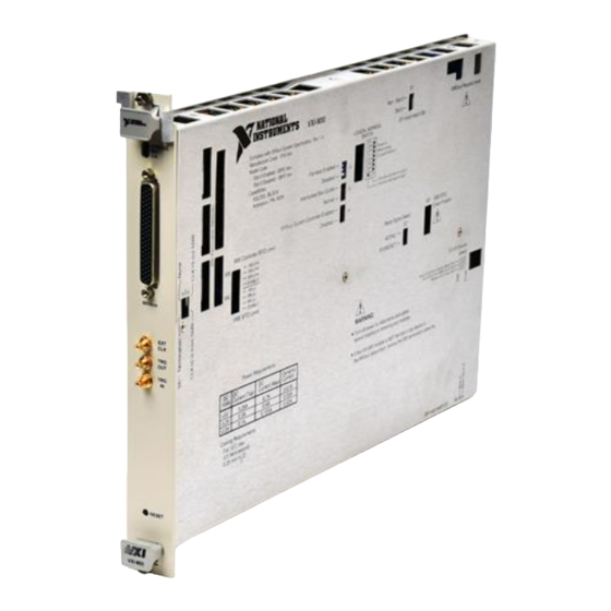
- Page 8 VXI-MXI Interface Module with INTX Option..........1-3 Figure 2-1. VXI-MXI Block Diagram................. 2-6 Figure 2-2. VXI-MXI INTX Daughter Card Option Block Diagram ......... 2-8 Figure 3-1. VXI-MXI Parts Locator Diagram..............3-2 Figure 3-2. VXI-MXI with INTX Parts Locator Diagram ..........3-3 Figure 3-3.
- Page 9 Figure 6-2. Deadlock Situation.................... 6-10 Figure C-1. VXI-MXI Parts Locator Diagram..............C-2 Figure C-2. VXI-MXI INTX Parts Locator Diagram (Rear View) ........C-3 Figure C-3. VXI-MXI INTX Parts Locator Diagram (Front View) ........C-4 Figure D-1. MXIbus Connector ................... D-1 Figure D-2.
-
Page 10: About This Manual
Chapter 5, Programming Considerations, explains important considerations for programming the VXI-MXI and configuring a system using VXI-MXIs. • Chapter 6, Theory of Operation, contains a functional overview of the VXI-MXI board and explains the operation of each functional block making up the VXI-MXI. •... -
Page 11: How To Use This Manual
About This Manual How to Use This Manual If you will be installing your VXI-MXI into a system with a VXIbus Resource Manager, you only need to read Chapters 1 through 3 of this manual. If you have more than two VXI-MXIs extending your system, you will find useful system configuration information in Chapter 5. -
Page 12: General Information
VXI-MXI interface module uses address mapping to transparently translate bus cycles on the VXIbus system bus (VMEbus) to the MXIbus and vice versa. The VXI-MXI is housed in a metal enclosure to improve EMI performance and to provide easy handling. Because the enclosure includes cut-outs to facilitate changes to switch and jumper settings, it should not be necessary to remove it under most circumstances. -
Page 15: Overview
The VXI-MXI is an extended class Register-Based VXIbus device with optional Slot 0 capability so that it can reside in any slot in a C-size or D-size VXIbus chassis. The VXI-MXI converts A32, A24, A16, D32, D16, and D08(EO) VXIbus bus cycles into MXIbus bus cycles and vice versa. -
Page 16: Front Panel Features
– 10 MHz clock – MODID register – TTL and ECL Trigger line support All integrated circuit drivers and receivers used on the VXI-MXI meet the requirements of both the VMEbus specification and the MXIbus specification. Front Panel Features The VXI-MXI has the following front panel features: •... -
Page 17: What Your Kit Should Contain
General Information Chapter 1 What Your Kit Should Contain Your VXI-MXI kit should contain the following components: Component Part Number Standard VXI-MXI Interface Module 181045-01 Enhanced VXI-MXI Interface Module with INTX option 181045-02 VXI-MXI User Manual 320222-01 Optional Equipment Equipment... -
Page 18: Unpacking
VXIbus mainframe chassis before removing the module from the bag. 4. As you remove the VXI-MXI module from its bag, be sure to handle it only by its edges. Avoid touching any of the IC components or connectors. Inspect the module for loose components or any other sign of damage. -
Page 19: Table 2-1. Vxi-Mxi Vmebus Signals
Electrical Characteristics All integrated circuit drivers and receivers used on the VXI-MXI meet the requirements of the VMEbus specification. Table 2-1 contains a list of the VMEbus signals used by the VXI-MXI and the electrical loading presented by the circuitry on the interface board (in terms of device types and their part numbers). -
Page 20: General Description
• VMEbus Master • VMEbus Slave • Interrupter • IACK Daisy-Chain Driver When the VXI-MXI is configured as a VXIbus Slot 0 device, it also has the following VMEbus modules: • VMEbus Timer • Arbiter • System Clock Driver VXI-MXI User Manual... -
Page 21: Table 2-3. Vxi-Mxi Vmebus Compliance Levels
Chapter 2 General Description The VXI-MXI does not support the following VMEbus modules: • Serial Clock Driver • Power Monitor Table 2-3 indicates the VXI-MXI VMEbus compliance levels. Table 2-3. VXI-MXI VMEbus Compliance Levels Compliance Notation Description Bus Slave Compliance Levels... - Page 22 General Description Chapter 2 Table 2-3. VXI-MXI VMEbus Compliance Levels (Continued) Compliance Notation Description Bus Master Compliance Levels D08(EO) 8-bit data path from MXIbus D16 & D08(EO) 8-bit or 16-bit data path from MXIbus 32-bit data path from MXIbus Generates 16-bit short I/O addresses when specified...
-
Page 23: Vxi-Mxi Functional Description
General Description VXI-MXI Functional Description In simplest terms, the VXI-MXI can be thought of as a bus translator that converts VXIbus signals into appropriate MXIbus signals. From the perspective of the MXIbus, the VXI-MXI implements a MXIbus interface to communicate with other MXIbus devices. From the perspective of the VMEbus, the VXI-MXI is an interface to the outside world. -
Page 24: Figure 2-1. Vxi-Mxi Block Diagram
Arbiter Circuitry Machine TTL Trigger Lines 7-0 TTL and ECL TRG OUT Trigger Lines TRG IN ECL Trigger Lines 1-0 CLK10 Circuitry CLK10 EXT CLK Front Panel SMBs Figure 2-1. VXI-MXI Block Diagram VXI-MXI User Manual © National Instruments Corporation... - Page 25 VXIbus, the MXIbus address/data lines are demultiplexed into separate VXIbus address and data lines. • MXIbus System Controller Functions If the VXI-MXI is the MXIbus System Controller, this circuitry provides the MXIbus arbiter, interrupt daisy-chain generation, and the MXIbus System Controller timeout logic. •...
-
Page 26: Figure 2-2. Vxi-Mxi Intx Daughter Card Option Block Diagram
General Description Chapter 2 The following information applies only to VXI-MXI kits that include the INTX daughter card option. Figure 2-2 is a block diagram of the circuitry of the INTX daughter card. INTX Registers Interrupt Control Trigger Control System Resets... - Page 27 VXIbus mainframe across the INTX connection, an interrupt handler in another VXIbus mainframe can generate an interrupt acknowledge cycle to handle that interrupt. The VXI-MXI in the requesting mainframe recognizes that the MXIbus interrupt acknowledge cycle is for the request it is...
-
Page 28: Configuration And Installation
• EXT CLK SMB Input/Output • Trigger Input Termination • Reset Signal Select If your VXI-MXI module includes the INTX daughter card option, you can also configure the following option: • CLK10 Mapping © National Instruments Corporation VXI-MXI User Manual... -
Page 31: The Metal Enclosure
VXIbus Slot 0 The VXI-MXI is shipped from the factory configured to be installed in Slot 0 of the VXIbus mainframe. If another device is already in Slot 0, you must decide which device will be the Slot 0 device and reconfigure the other device for Non-Slot 0 use. -
Page 32: Figure 3-4. Vxibus Non-Slot 0 Selection
VXIbus Model Code in the Device Type Register. If the VXIbus Model Code for the VXI-MXI is hex 00FE, the module is configured as a Slot 0 device; if the code is hex 08FE, the module is configured as a Non-Slot 0 device. -
Page 33: Vxibus Logical Address
The VXIbus RM has Logical Address 0 by definition. The VXI-MXI does not have VXIbus RM capability, so do not set the logical address for the VXI-MXI to 0. If you are configuring a multiple-mainframe VXIbus/MXIbus system, refer to Chapter 5, Programming Considerations, for instructions on planning a VXIbus/MXIbus system logical address map. -
Page 34: Figure 3-5. Logical Address Selection
VXIbus specification. Request level 3 is the highest priority request level and request level 0 is the lowest. You can change the VXI-MXI to use any of the other three request levels by changing the jumper configuration on the jumper blocks labeled VMEbus Request Level on the front panel. -
Page 35: Vmebus Request Level
In the case of multiple VXI-MXIs, it is recommended that the BTO be enabled on the VXI-MXI that is installed in Slot 0. The BTO monitors the current bus cycle and asserts the bus error (BERR) signal if a data transfer acknowledge (DTACK) or BERR is not received from the selected slave within the given amount of time after data strobe (DS1 or DS0) becomes active. -
Page 36: Figure 3-7. Vmebus Timeout Value Selection
VME BTO Chain Position jumper block selects how the VXIbus local bus is used to disable the VMEbus timeout when outward MXIbus transfers occur. If another device has a BTO module, remember to enable the BTO on the VXI-MXI and to disable the VMEbus BTO on the other device. -
Page 37: Vmebus Timeout Chain Position
When you have multiple VXI-MXI modules installed in adjacent slots, the VXIbus local bus is used to send a signal to the VXI-MXI with the VMEbus BTO to indicate that an outward MXIbus transfer is in progress. The following figures show how to configure the VME BTO Chain Position jumper block to select how the VXIbus local bus is used to disable the VMEbus timeout during outward MXIbus transfers. -
Page 38: Figure 3-9. Vmebus Timeout; Multiple Vxi-Mxis In Mainframe
Configuration and Installation If the system contains more than one VXI-MXI, select which card will supply the VMEbus timeout, and set the jumper block according to the VXI-MXI's position in relation to the adjacent VXI-MXIs. Figure 3-9 shows four possible settings. -
Page 39: Figure 3-10. No Vmebus Timeout; Multiple Vxi-Mxis In Mainframe
Configuration and Installation Chapter 3 For the VXI-MXIs that do not supply the VMEbus timeout, set the VME BTO Chain Position jumper block to reflect each VXI-MXI's position in relation to the adjacent VXI-MXIs. See Figure 3-10. VME BTO VME BTO... -
Page 40: Interlocked Arbitration Mode
Manager. In all the other mainframes, the VXI-MXIs must be the highest priority requesters. This means that a VXI-MXI should be installed in Slot 0 of its respective mainframe. In the case of multiple VXI-MXIs in a single mainframe, the additional VXI-MXIs should be installed in the slots adjacent to the Slot 0 VXI-MXI. -
Page 41: Mxibus System Controller
The VXI-MXI is shipped from the factory configured for non-MXIbus System Controller operation. If the VXI-MXI is the first device in the MXIbus link, configure the VXI-MXI as the MXIbus System Controller by changing the default setting of the slide switch from Disabled to Enabled, as shown in Figure 3-12. -
Page 42: Figure 3-12. Mxibus System Controller Selection
Chapter 3 Configuration and Installation MXIbus System Controller Enabled Disabled a. Not MXIbus System Controller (Default Setting) MXIbus System Controller Enabled Disabled b. MXIbus System Controller Figure 3-12. MXIbus System Controller Selection © National Instruments Corporation 3-15 VXI-MXI User Manual... -
Page 43: Mxibus System Controller Timeout
Figure 3-13 shows how to position the jumper array to set the MXIbus System Controller timeout value. When the VXI-MXI is not configured to be the MXIbus System Controller, the setting of this jumper array has no effect. Notice that when the LNGMXSCTO bit in the MXIbus Control Register is zero, the selected timeout value is in microseconds. -
Page 44: Mxibus Fairness Option
MXIbus chain. The MXIbus fairness feature is controlled by the Fairness slide switch. If you want your VXI-MXI to be a fair requester, change the slide switch from the Disabled setting to Enabled, as shown in Figure 3-14. -
Page 45: Clk10 Source
CLK10 Source Select jumper array to select one of these options, as shown in Figure 3-15. The VXI-MXI is configured at the factory to be a Slot 0 device driving the CLK10 signal from the onboard oscillator. If you are installing the VXI-MXI in a slot other than Slot 0, change the jumper array so that the VXI-MXI is configured to receive the CLK10 signal. -
Page 46: Figure 3-15. Clk10 Source Signal Options
Drive CLK10 from onboard 10MHz, Slot 0 Drive CLK10 from SMB CLK10, Slot 0 Receive CLK10, Non-Slot 0 c. Do Not Source CLK10; VXI-MXI Not Installed in Slot 0 CLK10 Source Select Drive CLK10 from onboard 10MHz, Slot 0 Drive CLK10 from SMB CLK10, Slot 0 Receive CLK10, Non-Slot 0 d. -
Page 47: Ext Clk Smb Input/Output
CLK10 signals of the two mainframes together using the EXT CLK SMB connectors on the front panel of the VXI-MXI. One mainframe should source the CLK10 signal to the SMB connection. The other device receives the CLK10 signal from the SMB connection and drives it on the VXIbus CLK10 lines. -
Page 48: Figure 3-17. Intx Clk10 Mapping Switches
(W9 and W10 must be removed) Do Not Drive CLK10 from INTX CLK10 Receive CLK10 from INTX INTX CLK10 Routing Drive CLK10 out INTX c. CLK10 Mapped into Mainframe Figure 3-17. INTX CLK10 Mapping Switches © National Instruments Corporation 3-21 VXI-MXI User Manual... -
Page 49: Trigger Input Termination
Configuration and Installation Chapter 3 The VXI-MXI must be installed in Slot 0 if you want to route the INTX CLK10 signal to the VXIbus CLK10 signal. The CLK10 Source Select jumpers on the VXI-MXI must be set to configure the VXI-MXI to receive the CLK10 because the INTX daughter card will now be sourcing the clock signal. -
Page 50: Reset Signal Select
Configuration and Installation Reset Signal Select The VXI-MXI generates a 200 ms active low pulse both on power-up and when you press the pushbutton system reset switch on the front panel. Using the Reset Signal Select slide switch, you can route the pulse to either VMEbus signal ACFAIL* or SYSRESET*. See Figure 3-19. -
Page 51: Mxibus Termination
TERMPWR is not intended to provide power to any other device. The VXI-MXI is shipped from the factory with terminating SIP resistor networks installed. If the VXI-MXI will be the first or last device in the MXIbus daisy-chain and external terminating VXI-MXI User Manual 3-24 ©... -
Page 53: Installation Instructions
Verify the following configuration considerations before installing the VXI-MXI: • If installing the VXI-MXI in a slot other than Slot 0, verify that you have changed the settings of the two VXIbus Slot 0 slide switches, the VME BTO Chain Position jumper, and the CLK10 Source Select jumpers. -
Page 54: Connecting The Intx Cable
C-size cards in D-size mainframes. 4. Insert the VXI-MXI into the slot of the mainframe by aligning the top and bottom of the card with the card guides inside the mainframe. Slowly push the VXI-MXI straight into the slot until it seats in the backplane receptacles. -
Page 57: System Power Cycling Requirements
When shutting down a system, you must ensure that all devices that could be adversely affected by unintended bus cycles or interrupts have their windows and interrupt mapping disabled. The VXI-MXI itself will not be affected during power-down; however, there may be devices in the same frame as the VXI-MXI that could be affected. -
Page 58: Vmebus Devices In Vxibus/Mxibus Systems
FFFF hex) of A16 space, you need to indicate to the system Resource Manager that there are non-VXIbus foreign devices installed. Be careful not to configure any static VXIbus logical addresses in the portions of A16 space occupied by the VMEbus devices. © National Instruments Corporation 3-31 VXI-MXI User Manual... -
Page 59: Register Descriptions
VMEbus SYSRESET signal is active. A hard reset clears all the registers on the VXI-MXI. A soft reset occurs when the RESET bit in the VXIbus Control Register is set. A soft reset clears signals that are asserted by bits in the configuration registers but does not clear configuration information stored in the configuration registers. -
Page 60: Table 4-1. Vxi-Mxi Register Map
* The three INTX registers at offsets 12, 14, and 18 are only available on VXI-MXIs with the INTX daughter card option. On VXI-MXIs without the INTX option, the entire range between offsets 12 and 1C (inclusive) is VXI-MXI Reserved Space. VXI-MXI User Manual... -
Page 61: Figure 4-1. Vxi-Mxi Register Map
A24 Window Map Register A16 Window Map Register Logical Address Window MODID Register Reserved Basic VXI VXIbus Status / Control Configuration Device Type Registers VXIbus ID Register 16-bit Words Figure 4-1. VXI-MXI Register Map © National Instruments Corporation VXI-MXI User Manual... -
Page 62: Vxibus Configuration Registers
These bits indicate the device class of the VXIbus device as follows: 00 = Memory 01 = Extended 10 = Message-Based 11 = Register-Based The VXI-MXI is an extended device defined by National Instruments; therefore, these bits are configured in hardware as binary 01. 13-12r ADDR Address Space Bits... - Page 63 11-0r MANID Manufacturer ID Bits This number uniquely identifies the manufacturer of the VXIbus device. These bits are configured in hardware as hex FF6, the VXIbus manufacturer ID number assigned to National Instruments. © National Instruments Corporation VXI-MXI User Manual...
-
Page 64: Device Type Register
Slot 0 devices. When the VXI-MXI is in Slot 0, bit 11 is 0 and its model code is hex 00FE. When the VXI-MXI is not in Slot 0, bit 11 is 1 and its model code is hex 08FE. -
Page 65: Vxibus Status/Control Register
This register provides status information about this VXIbus device and provides a bit to force the VXI-MXI into a Soft Reset state. The RESET bit is cleared on a hard reset. Hard and soft resets have no effect on the other bits on this register. - Page 66 RESET Reset Bit When this bit is set, the VXI-MXI is forced into the Soft Reset state. When this bit is cleared, the VXI-MXI is in the normal operation state. This bit is readable and is cleared on a hard reset.
-
Page 67: Vxibus Extender Registers
MODID6 MODID5 MODID4 MODID3 MODID2 MODID0 This register provides control and status of the MODID lines when the VXI-MXI is installed in Slot 0. Mnemonic Description 15-14r/w 0 Reserved Bits These bits are reserved and read back as zeros. Write a zero when writing to these bits. -
Page 68: Logical Address Window Register
Attributes: Read/Write This register defines the range of logical addresses that are mapped into and out of the VXI-MXI through the MXIbus. This register defines a configuration window in the upper 16 KB of A16 space. These bits are cleared on a hard reset. - Page 69 Logical Address Window Base Address Bits These bits, in conjunction with the LASIZE bits, define the base address of the Logical Address window for the VXI-MXI. The LASIZE bits indicate the number of LABASE bits that are most significant. LABASE7 is the most significant, and LABASE0 is the least.
- Page 70 LAHIGH > range LALOW The VXIbus logical addresses mapped out of the VXI-MXI are the inverse of this range, that is, MXIbus logical addresses greater than or equal to the LAHIGH value or less than the LALOW value.
- Page 71 To accommodate 8-bit devices that write to this register, the window is not enabled until the lower byte of the register is written. Therefore, 8-bit devices should write the upper byte first, then the lower byte. © National Instruments Corporation 4-13 VXI-MXI User Manual...
-
Page 72: A16 Window Map Register
This register defines the range of addresses in the lower 48 KB of A16 space that is mapped into and out of the VXI-MXI through the MXIbus. Earlier versions of the VXI-MXI required the A16 window to be statically configured with a DIP switch. Now the A16 window can only be dynamically configured with this register. - Page 73 A16 Window Base Address Bits These bits, in conjunction with the A16SIZE bits, define the base address of the A16 window for the VXI-MXI. The A16SIZE bits indicate the number of A16BASE bits that are most significant. A16BASE7 is the most significant and A16BASE0 is the least.
- Page 74 A16HIGH > range A16LOW The VXIbus A16 addresses mapped out of the VXI-MXI are the inverse of this range, that is, MXIbus A16 addresses greater than or equal to the A16HIGH value or less than the A16LOW value.
- Page 75 To accommodate 8-bit devices that write to this register, the window is not enabled until the lower byte of the register is written. Therefore, 8-bit devices should write the upper byte first, then the lower byte. © National Instruments Corporation 4-17 VXI-MXI User Manual...
-
Page 76: A24 Window Map Register
This register defines the range of addresses in A24 space that are mapped into and out of the VXI-MXI through the MXIbus. These bits are cleared on a hard reset. The CMODE bit in the MXIbus Control Register selects the format of this register. If the CMODE bit is 0 (default), a Base/Size window comparison is used to determine the range of addresses in the window. - Page 77 A24 Window Base Address Bits These bits, in conjunction with the A24SIZE bits, define the base address of the A24 window for the VXI-MXI. The A24SIZE bits indicate the number of A24BASE bits that are most significant. A24BASE7 is the most significant and A24BASE0 is the least.
- Page 78 A24HIGH > range A24LOW The VXIbus A24 addresses mapped out of the VXI-MXI are the inverse of this range, that is, MXIbus A24 addresses greater than or equal to the A24HIGH value or less than the A24LOW value.
- Page 79 To accommodate 8-bit devices that write to this register, the window is not enabled until the lower byte of the register is written. Therefore, 8-bit devices should write the upper byte first, then the lower byte. © National Instruments Corporation 4-21 VXI-MXI User Manual...
-
Page 80: A32 Window Map Register
This register defines the range of addresses in A32 space that are mapped into and out of the VXI-MXI through the MXIbus. These bits are cleared on a hard reset. The CMODE bit in the MXIbus Control Register selects the format of this register. If the CMODE bit is 0 (default), a Base/Size window comparison is used to determine the range of addresses in the window. - Page 81 A32 Window Base Address Bits These bits, in conjunction with the A32SIZE bits, define the base address of the A32 window for the VXI-MXI. The A32SIZE bits indicate the number of A32BASE bits that are most significant. A32BASE7 is the most significant and A32BASE0 is the least.
- Page 82 A32HIGH > range A32LOW The VXIbus A32 addresses mapped out of the VXI-MXI are the inverse of this range, that is, MXIbus A32 addresses greater than or equal to the A32HIGH value or less than the A32LOW value.
- Page 83 To accommodate 8-bit devices that write to this register, the window is not enabled until the lower byte of the register is written. Therefore, 8-bit devices should write the upper byte first, then the lower byte. © National Instruments Corporation 4-25 VXI-MXI User Manual...
-
Page 84: Intx Interrupt Configuration Register
INTX IRQ line. If the EINTxDIR bit is set, the INTX IRQ line drives the corresponding VMEbus IRQ line. EINTxEN EINTxDIR Routing Disabled VME IRQ X drives INTX IRQ INTX IRQ drives VME IRQ X VXI-MXI User Manual 4-26 © National Instruments Corporation... -
Page 85: Intx Trigger Configuration Register
If the ETRGxDIR bit is set, the INTX trigger drives the corresponding VXIbus TTL trigger line. ETRGxEN ETRGxDIR Routing Disabled VXI trigger X drives INTX trigger line X INTX trigger line X drives VXI trigger X © National Instruments Corporation 4-27 VXI-MXI User Manual... -
Page 86: Intx Utility Configuration Register
VXIbus P2 ECL trigger lines. Extended Utility Line Support This bit is set in hardware to zero to indicate that the INTX daughter card supports this Utility Configuration register. VXI-MXI User Manual 4-28 © National Instruments Corporation... - Page 87 Setting this bit enables the VMEbus SYSRESET line to be mapped out onto the INTX SYSRESET line. Clearing this bit disables the mapping of the SYSRESET line onto the INTX SYSRESET line. This bit is cleared on power-up. © National Instruments Corporation 4-29 VXI-MXI User Manual...
-
Page 88: Subclass Register
Attributes: Read only SUBCLASS These bits define the subclass of a VXIbus extended device. The VXI-MXI is a VXIbus Mainframe Extender. Such devices are assigned the subclass code hex FFFC. Hard and soft resets have no effect on this register. -
Page 89: Mxibus Defined Registers
Read/Modify Write Select Mode Bit This bit, along with the MXIbus Address Modifiers, selects how the VXI-MXI will treat a MXIbus cycle when the MXIbus Address Strobe is held low for multiple data transfers. This bit is cleared on hard and soft resets. - Page 90 Trigger Out SMB on the front panel. This bit is cleared on a hard reset. ECLxEN ECLxDIR Routing Disabled ECL Trigger Line X drives TRIG OUT SMB TRIG IN SMB drives ECL Trigger Line X VXI-MXI User Manual 4-32 © National Instruments Corporation...
- Page 91 MXSCTO MXIbus System Controller Timeout Status Bit If this VXI-MXI is the MXIbus System Controller, this bit is set if the VXI-MXI sent a MXIbus BERR on the last MXIbus transfer in response to a MXIbus System Controller Timeout. This bit is cleared when this register is read and on hard and soft resets.
- Page 92 FAIR VXI-MXI Fairness Status Bit When this bit is set, the VXI-MXI is configured as a fair MXIbus requester. If this bit is cleared, the VXI-MXI is configured as an unfair MXIbus requester. FAIR is selected with slide switch S2.
- Page 93 3r/w LNGMXSCTO Long MXIbus System Controller Timeout Bit When the VXI-MXI powers on, this bit is cleared and, if the VXI-MXI is the MXIbus System Controller, the MXIbus System Controller timeout is between 100 µs and 400 µs (selected by jumper W8).
-
Page 94: Mxibus Lock Register
Lock MXIbus or VXIbus Bit When this bit is set by a VXIbus device, the MXIbus is locked by that device as soon as the MXIbus is won by the VXI-MXI. When the MXIbus is locked, indivisible operations to remote resources can be performed across the MXIbus. -
Page 95: Mxibus Irq Configuration Register
IRQ line, the selected VMEbus IRQ lines are ORed together and the result drives the MXIbus IRQ line. If the MIRQxDIR bit is set, the MXIbus IRQ line drives the corresponding VMEbus IRQ line. © National Instruments Corporation 4-37 VXI-MXI User Manual... - Page 96 Register Descriptions Chapter 4 MIRQxEN MIRQxDIR Routing Disabled VME IRQ X drives MXI IRQ MXI IRQ drives VME IRQ X VXI-MXI User Manual 4-38 © National Instruments Corporation...
-
Page 97: Drive Triggers/Read La Register
DRVECL1 DRVECL0 PULSE This register provides the logical address of the VXI-MXI and the status of the eight TTL Trigger lines on the VXIbus. This register is also used to drive the TTL and ECL Trigger lines individually. The bits in this register are cleared on hard and soft resets. - Page 98 10 MHz clock. DRVECL0 Drive ECL Trigger Line 0 Setting this bit asserts the VXIbus ECL Trigger Line 0 after synchronizing the signal with the 10 MHz clock. VXI-MXI User Manual 4-40 © National Instruments Corporation...
-
Page 99: Trigger Mode Selection Register
These bits select which trigger protocol or signal is driven on the trigger line specified by the OTS[3-0] bits. OMS2 OMS1 OMS0 Trigger Output Mode Disabled Sync, Semi-Sync, or Async Source Start-Stop Source Semi-Sync Acceptor Source from TRIG IN SMB Reserved Reserved © National Instruments Corporation 4-41 VXI-MXI User Manual... - Page 100 TTL Trigger Line 2 TTL Trigger Line 3 TTL Trigger Line 4 TTL Trigger Line 5 TTL Trigger Line 6 TTL Trigger Line 7 Reserved ECL Trigger Line 0 ECL Trigger Line 1 Reserved Reserved VXI-MXI User Manual 4-42 © National Instruments Corporation...
- Page 101 Trigger Input Status Bit If this bit is set, the signal input from the Trigger In SMB connector on the front panel is high. If this bit is cleared, that input signal is low. © National Instruments Corporation 4-43 VXI-MXI User Manual...
- Page 102 SSIE Synchronous Interrupt Enable Bit When this bit is set, an interrupt request is generated when the trigger line selected by the ITS[3-0] bits changes from asserted to unasserted (low to high). VXI-MXI User Manual 4-44 © National Instruments Corporation...
-
Page 103: Interrupt Status/Control Register
Description 15-13r/w LINT[3-1] Local Interrupt Line Bits These bits select the VMEbus interrupt request line onto which the local VXI-MXI interrupts are routed. The local interrupts are BKOFF, TRIGINT, ACFAIL, and SYSFAIL. LINT3 LINT2 LINT1 VMEbus Interrupt Request Line Local Interrupt Disabled... - Page 104 SYSFAILIE VXIbus SYSFAIL Interrupt Enable Bit If this bit is set, an interrupt is generated on the VMEbus interrupt line selected by the LINT[3-1] bits when the VXIbus SYSFAIL line is set. VXI-MXI User Manual 4-46 © National Instruments Corporation...
- Page 105 Setting these bits drives the corresponding VMEbus IRQ lines. When the VMEbus IRQ line driven by one of these bits is serviced by an VMEbus interrupt acknowledge cycle, the corresponding bit is cleared. © National Instruments Corporation 4-47 VXI-MXI User Manual...
-
Page 106: Status/Id Register
DIRQ bits in the Interrupt Control Register. This register powers up to an indeterminate value and is not cleared on either a hard or soft reset. VXI-MXI User Manual 4-48 © National Instruments Corporation... -
Page 107: Mxibus Trigger Configuration Register
TRIG7DIR TRIG6DIR TRIG5DIR TRIG4DIR TRIG3DIR TRIG2DIR TRIG1DIR TRIG0DIR This register maps the VXIbus TTL Trigger lines to and from the Trigger In and Trigger Out SMB connectors on the front panel of the VXI-MXI. These bits are cleared on a hard reset. Mnemonic... -
Page 108: Trigger Synchronous Acknowledge Register
Writing any value to this register reinitializes the SSINT* bit in the Trigger Mode Selection Register. Trigger Asynchronous Acknowledge Register VXIbus Address: Base Address + 36 (hex) Attributes: Write Only Writing any value to this register reinitializes the ASINT* bit in the Trigger Mode Selection Register. VXI-MXI User Manual 4-50 © National Instruments Corporation... -
Page 109: Irq Acknowledge Registers
MXIbus. Each VMEbus IRQ line has a separate interrupt acknowledge register, as shown above in the VXIbus Address. The value returned when these registers are read by a VMEbus device is hex FFFF. © National Instruments Corporation 4-51 VXI-MXI User Manual... -
Page 110: Programming Considerations
Notice that only one MXIbus link can be connected on the first level below a root PC multiframe RM, while multiple MXIbus links can be connected on the first level below a root VXIbus mainframe. © National Instruments Corporation VXI-MXI User Manual... -
Page 111: Figure 5-1. Vxibus/Mxibus System With Multiframe Rm On A Pc
Figure 5-1. VXIbus/MXIbus System with Multiframe RM on a PC Multiframe Resource VXIbus Root Manager Mainframe VXIbus VXIbus MXIbus MXIbus Level 1 Mainframe Mainframe Device Device Level 2 VXIbus Mainframe Figure 5-2. VXIbus/MXIbus System with Multiframe RM in a VXIbus Mainframe VXI-MXI User Manual © National Instruments Corporation... -
Page 112: Base/Size Configuration Format
MXIbus link. The address mapping windows on the VXI-MXI can be configured to have a Base/Size format or a High/Low format. The CMODE bit in the MXIbus Control Register selects which format the mapping windows use. -
Page 113: Figure 5-3. Base And Size Combinations
5F-50 4F-40 3F-30 Size = 3 2F-20 1F-10 Size = 4 0F-00 Size = 5 Size = 6 Size = 7 Size = 8 Figure 5-4. Address Range Allocation for Different Size Values VXI-MXI User Manual © National Instruments Corporation... -
Page 114: High/Low Configuration Format
VXIbus mainframe on Level 1, you must change the logical addresses of both VXI-MXI interfaces so that they are not at the default of 1. Select a logical address that is greater than or equal to the number of logical addresses required by the mainframe. - Page 115 If you are using Base/Size parameters, determine the Size field of the range for each device and MXIbus link and insert that value in the corresponding locations of the worksheets. When you round up the number of logical addresses required to 2 , Size = 8 – X. VXI-MXI User Manual © National Instruments Corporation...
- Page 116 In the example system, we assigned MXIbus #3 address range A0 to BF hex. MXIbus #3 has two devices: VXIbus Mainframe #4 and VXIbus Mainframe #5. Each requires 16 logical addresses; therefore, we assigned them address ranges A0 to AF hex, and B0 to BF hex, respectively. © National Instruments Corporation VXI-MXI User Manual...
-
Page 117: Figure 5-5. Example Vxibus/Mxibus System
Table 5-2. Example VXIbus/MXIbus System Required Logical Addresses Number of Logical Device Addresses Required VXIbus Mainframe #1 MXIbus Device A MXIbus Device B VXIbus Mainframe #2 VXIbus Mainframe #3 VXIbus Mainframe #4 VXIbus Mainframe #5 VXIbus Mainframe #6 VXI-MXI User Manual © National Instruments Corporation... -
Page 118: Figure 5-6. Logical Address Map Diagram For Example Vxibus/Mxibus System
9F-90 Mainframe #3 VXIbus Mainframe #3 8F-80 7F-70 6F-60 5F-50 4F-40 3F-30 2F-20 1F-10 VXIbus Mainframe #6 MXIbus #2 0F-00 VXIbus Mainframe #1 Figure 5-6. Logical Address Map Diagram for Example VXIbus/MXIbus System © National Instruments Corporation VXI-MXI User Manual... -
Page 119: Figure 5-7. Worksheet 1 For Example Vxibus/Mxibus System
Round total number up to next power of two: Size = 8-8 = 0 (If this number is greater than 256, you need to reorganize devices and try again.) Figure 5-7. Worksheet 1 for Example VXIbus/MXIbus System VXI-MXI User Manual 5-10 © National Instruments Corporation... -
Page 120: Figure 5-8. Worksheet 2 For Example Vxibus/Mxibus System
– (Add numbers after the "*") Range = Round total number up to next power of two: 128 (2 Size = 8-7 = 1 Figure 5-8. Worksheet 2 for Example VXIbus/MXIbus System © National Instruments Corporation 5-11 VXI-MXI User Manual... -
Page 121: Figure 5-9. Worksheet 3 For Example Vxibus/Mxibus System
– (Add numbers after the "*") Range = Round total number up to next power of two: 32 (2 Size = 8-5 = 3 Figure 5-10. Worksheet 4 for Example VXIbus/MXIbus System VXI-MXI User Manual 5-12 © National Instruments Corporation... -
Page 122: Worksheets For Planning Your Vxibus/Mxibus Logical Address Map
F E D C B A 9 8 7 6 5 4 3 2 1 0 FF-F0 EF-E0 DF-D0 CF-C0 BF-B0 AF-A0 9F-90 8F-80 7F-70 6F-60 5F-50 4F-40 3F-30 2F-20 1F-10 0F-00 © National Instruments Corporation 5-13 VXI-MXI User Manual... - Page 123 (Add numbers after the "*") Range = Round total number up to next power of two: Size = (If this number is greater than 256, you need to reorganize devices and try again.) VXI-MXI User Manual 5-14 © National Instruments Corporation...
- Page 124 Round total number up to the next power of two: Size = Total Number of Logical Addresses Required: (Add numbers after the "*") Range = Round total number up to next power of two: Size = © National Instruments Corporation 5-15 VXI-MXI User Manual...
- Page 125 Round total number up to the next power of two: Size = Total Number of Logical Addresses Required: (Add numbers after the "*") Range = Round total number up to next power of two: Size = VXI-MXI User Manual 5-16 © National Instruments Corporation...
- Page 126 Round total number up to the next power of two: Size = Total Number of Logical Addresses Required: (Add numbers after the "*") Range = Round total number up to next power of two: Size = © National Instruments Corporation 5-17 VXI-MXI User Manual...
-
Page 127: Alternative Worksheets For Planning Your Vxibus/Mxibus Logical Address Map
Figure 5-5. Notice that the system does not take up as much of the logical address space as the Base/Size method of configuration because address requirements do not have to occupy blocks in powers of two. With High/Low configuration, each VXI-MXI window can be configured for exactly the amount of address space the mainframe needs. -
Page 128: Figure 5-11. Logical Address Map Example With Alternative Worksheet
Range IN Range IN Range IN Range IN Range IN Range OUT Range OUT Range OUT Range OUT Range OUT Range OUT Range OUT Figure 5-11. Logical Address Map Example with Alternative Worksheet © National Instruments Corporation 5-19 VXI-MXI User Manual... -
Page 129: Planning A Vxibus/Mxibus System A16 Address Map
Table 5-3. Amount of A16 Space Allocated for all Size Values Amount of A16 Space Allocated Size (in Bytes) 512 B 1 KB 2 KB 4 KB 8 KB 16 KB 32 KB 48 KB (All of A16 space) © National Instruments Corporation 5-21 VXI-MXI User Manual... -
Page 130: Figure 5-12. A16 Space Allocations For All Size Values
Table 5-3. Next, assign the A16 space, starting with the root device and working down the VXIbus/MXIbus system tree. To assist you in configuring the A16 window switches on the VXI-MXI interfaces in your system, the following pages include worksheets, an address map diagram, and an example. - Page 131 9. The next step is to determine the range of addresses, or base address, size, and direction of the A16 window for each VXI-MXI in the system. We first assign A16 space to the VXIbus RM Mainframe. From Figure 5-15, we see it needs 16 KB of A16 space, so we assign it the bottom 16 KB of A16 space, addresses 0 through 3FFF hex.
-
Page 132: Figure 5-13. Example Vxibus/Mxibus System
Programming Considerations Chapter 5 5000 through 5FFF to MXIbus #3. For the VXI-MXI connected to MXIbus #3, we set Base = 5000, Size = 4 because 4 KB = 256 * 2 , and the direction toward MXIbus #3, or Out. -
Page 133: Figure 5-14. Example A16 Space Address Map
VXIbus Mainframe #6 8FFF-8000 7FFF-7000 MXIbus Device A 6FFF-6000 MXIbus #1 VXIbus Mainframe #4 5FFF-5000 VXIbus Mainframe #3 4FFF-4000 3FFF-3000 VXIbus Mainframe #1 2FFF-2000 1FFF-1000 0FFF-0000 Figure 5-14. Example A16 Space Address Map © National Instruments Corporation 5-25 VXI-MXI User Manual... -
Page 134: Figure 5-15. Worksheet 1 For A16 Address Map Example
Amount of A16 space required for this mainframe: Round up to next address break: MXIbus #1 First Level MXIbus Link: 8 KB + 512 Amount of A16 space required for devices connected to this VXI-MXI: Round up to next address break: 4000 A16 Window: Base: Size:... -
Page 135: Figure 5-16. Worksheet 2 For A16 Map Example
Total amount of A16 space required for this window: Round up total amount to the next address size break: First Level VXI-MXI: A16 Window: Base: Size: Direction: Second Level VXI-MXI #1: A16 Window: Base: Size: Direction: Second Level VXI-MXI #2: A16 Window: Base:... -
Page 136: Figure 5-17. Worksheet 3 For A16 Map Example
Total amount of A16 space required for this window: Round up total amount to the next address size break: First Level VXI-MXI: 5000 A16 Window: Base: Size: Direction: Second Level VXI-MXI #1: A16 Window: Base: Size: Direction: Second Level VXI-MXI #2: A16 Window: Base: Size:... -
Page 137: Worksheets For Planning Your Vxibus/Mxibus A16 Address Map
MXIbus system. Follow the procedures used to fill out the worksheets for the sample VXIbus/ MXIbus system. C0 B0 A0 90 80 50 40 30 20 10 F0 E0 BFFF-B000 AFFF-A000 9FFF-9000 8FFF-8000 7FFF-7000 6FFF-6000 5FFF-5000 4FFF-4000 3FFF-3000 2FFF-2000 1FFF-1000 0FFF-0000 © National Instruments Corporation 5-29 VXI-MXI User Manual... - Page 138 Resource Manager Mainframe: Amount of A16 space required for this mainframe: Round up to next address break: First Level MXIbus Link: Amount of A16 space required for devices connected to this VXI-MXI: Round up to next address break: A16 Window: Base: Size:...
- Page 139 Total amount of A16 space required for this window: Round up total amount to the next address size break: First Level VXI-MXI: A16 Window: Base: Size: Direction: Second Level VXI-MXI #1: A16 Window: Base: Size: Direction: Second Level VXI-MXI #2: A16 Window: Base:...
- Page 140 Total amount of A16 space required for this window: Round up total amount to the next address size break: First Level VXI-MXI: A16 Window: Base: Size: Direction: Second Level VXI-MXI #1: A16 Window: Base: Size: Direction: Second Level VXI-MXI #2: A16 Window: Base:...
- Page 141 Total amount of A16 space required for this window: Round up total amount to the next address size break: First Level VXI-MXI: A16 Window: Base: Size: Direction: Second Level VXI-MXI #1: A16 Window: Base: Size: Direction: Second Level VXI-MXI #2: A16 Window: Base:...
- Page 142 Total amount of A16 space required for this window: Round up total amount to the next address size break: First Level VXI-MXI: A16 Window: Base: Size: Direction: Second Level VXI-MXI #1: A16 Window: Base: Size: Direction: Second Level VXI-MXI #2: A16 Window: Base:...
-
Page 143: Multiframe Rm Operation
VXIbus ID Register. If two devices share a logical address, they will both respond to an address access without any indication of an error. B. For each VXI-MXI found in the mainframe, starting with the lowest addressed VXI-MXI, the RM: Sets the VXI-MXI logical address window to map all of the logical address space outward and enables the window. -
Page 144: Configuring The Logical Address Window Example
Repeats Step 2 recursively. c. Sets the VXI-MXI inward logical address mapping window to cover the range up to (but not including) the VXI-MXI with the next highest logical address that was found in the logical address space. Sets the VXI-MXI outward logical address mapping window to cover the range of the devices connected to that extender. - Page 145 VXI-MXIs at logical addresses 2 and 4 and moves DC devices to the lowest unused logical addresses (for example, 1, 3, 5, 6). 2. Enables the logical address window of the VXI-MXI found at logical address 2 for the entire outward mapping range of 0 to FF. Scans all logical addresses, skipping all previously encountered devices, and finds the VXI-MXI in VXIbus Mainframe #3, the VXI-MXI in VXIbus Mainframe #2, MXIbus Device A, and MXIbus Device B.
-
Page 146: Configuring The A24 And A32 Addressing Windows
Device A (E0 to E3), and MXIbus Device B (E4). Enables the logical address window of the VXI-MXI at logical address 2 with an outward range of 80 to FF by writing the value 4180 hex to the Logical Address Window Register (Base/Size format). -
Page 147: System Administration And Initiation
VXIbus specification. A general-purpose multiframe RM must wait five seconds before testing the Passed condition of each device, because no prescribed global mechanism is defined for monitoring all of the SYSFAIL signals in the system. © National Instruments Corporation 5-39 VXI-MXI User Manual... -
Page 148: Chapter 6 Theory Of Operation
MODID lines. In accordance with the VXIbus specification for a Slot 0 device, the VXI-MXI pulls up each MODID line with a 16.9 k resistor. When the VXI-MXI is not a Slot 0 device, the MODID0 line is pulled to ground with a 825 resistor. -
Page 149: Vmebus Control Signals Transceivers
VMEbus. When the LOCK bit in the Local Bus Lock Register is set by a MXIbus device, the VXI-MXI interface will not release the VMEbus once it is granted the bus (on the next transaction) until the LOCK bit is cleared by a MXIbus device. -
Page 150: Sysfail, Acfail, And Sysreset
When asserted, the trigger line indicates a Start signal. When unasserted, the trigger line indicates a Stop signal. The VXI-MXI can be configured either to drive its 10 MHz VXIbus CLK10 signal to other mainframes or to receive a 10 MHz CLK10 signal from another mainframe via the EXT CLK SMB connector on the front panel. - Page 151 VMEbus interrupt requests can be handled by an interrupt handler on another VMEbus device in the VXIbus mainframe or by an external device on the MXIbus. The VXI-MXI has IACK daisy- chain driver circuitry that passes interrupt acknowledge cycles not meant for the VXI-MXI to other interrupters in the VXIbus mainframe.
-
Page 152: Table 6-1. Vxi-Mxi Addresses For Vmebus Interrupt Levels
VXIbus mainframe by reading from a designated address in the MXIbus configuration space on the remote VXI-MXI. The external device must know which VMEbus interrupt level it is servicing and read from the appropriate address. Table 6-1 shows the designated addresses for VMEbus IRQ[7–1]. -
Page 153: Parity Check And Generation
VXI-MXI Configuration Registers The VXI-MXI configuration registers are accessible from both the VXIbus and the MXIbus and are used to configure the VXI-MXI. These registers are described in detail in Chapter 4, Register Descriptions. When the VXI-MXI interface decodes a VMEbus address specifying the configuration space on the card, the least significant VMEbus address lines are used to specify the registers in configuration space and the VMEbus operation does not need to request control of the MXIbus. -
Page 154: Table 6-2. Vmebus To Mxibus Address Modifier Line Map
The VMEbus address lines map directly to the MXIbus address lines. The VMEbus requires six address modifier lines, while MXIbus only defines five. The VMEbus address modifier lines map to the MXIbus address modifier lines as shown in Table 6-2. The VXI-MXI responds to the VMEbus address modifier codes shown in Table 6-3. -
Page 155: Table 6-3. Transfer Responses For Vmebus Address Modifiers
0 (AD01 and AD00). The VMEbus transfer size information is converted into MXIbus transfer size information during a MXIbus master transfer. Table 6-4 compares this information for the VMEbus and the MXIbus. VXI-MXI User Manual © National Instruments Corporation... -
Page 156: Table 6-4. Vmebus/Mxibus Transfer Size Comparison
The MXIbus PAR* signal is generated and sent during the address portion of all MXIbus cycles initiated by the VXI-MXI. It is also generated and sent during the data portion of MXIbus master write cycles. When the VXI-MXI detects a parity error in the data transfer portion of a MXIbus read cycle, it asserts the VMEbus BERR* signal to indicate to the VMEbus host that the data read contains an error. -
Page 157: Mxibus Slave Mode State Machine
Mainframe VMEbus VMEbus Figure 6-2. Deadlock Situation If the VXI-MXI responds with a VMEbus BERR* to a transfer initiated by a VXIbus device, the transfer was not completed successfully. The following situations are possible reasons for an unsuccessful transfer: •... -
Page 158: Mxibus Address/Data And Address Modifier Transceivers
MXIbus cycles. The VMEbus is not requested if the MXIbus address received has a parity error. Parity is also checked when MXIbus data is written to the VXI-MXI slave circuitry. If a parity error occurs, the bad data is not written to the VMEbus and a BERR is sent back to the MXIbus master. -
Page 159: Mxibus System Controller Functions
An onboard slide switch sets whether or not the VXI-MXI interface board is the MXIbus System Controller. If it is the system controller, the VXI-MXI must be the first device in the MXIbus daisy-chain. Onboard arbitration circuitry transparently performs the MXIbus arbitration for the MXIbus chain. - Page 160 MXIbus. When the LOCK bit in the Local Bus Lock Register is set by a VXIbus device, the VXI-MXI interface will not release the MXIbus the next time it is granted the bus (on the next transaction) until the LOCK bit is cleared by a VXIbus device.
- Page 161 Theory of Operation Chapter 6 For example, if the VXI-MXI owns the VMEbus and it receives a VMEbus bus request from another VXIbus device, the VXI-MXI continues holding the VMEbus and arbitrates for the MXIbus. When it wins the MXIbus, the VXI-MXI can then release the VMEbus so that another VMEbus requester can gain ownership of the VMEbus.
-
Page 162: Appendix A Specifications
IACK IACK daisy-chain driver VXIbus Capability Code Description TRIG+1 Supports TTLTRIG0:7 and ECLTRIG0:1 trigger lines and full protocol operations for each. The VXI-MXI may participate in only one protocol operation at a time. © National Instruments Corporation VXI-MXI User Manual... - Page 163 Component temperature 0° to 70° C operating; -40° to 85° C storage Airflow 3.5 liters/s for 10° rise Relative humidity 10% to 90% noncondensing operating; 0% to 95% noncondensing storage Emissions FCC Class A VXI-MXI User Manual © National Instruments Corporation...
- Page 164 381 ns Block Write 320 ns Block Write 238 ns Block Read 270 ns Block Read 238 ns Other Daisy-Chain Delay 120 ns (Passing GIN to GOUT or GOUT generation from System Controller) © National Instruments Corporation VXI-MXI User Manual...
-
Page 165: Appendix B Mnemonics Key
MXIbus, VMEbus, VXIbus, and register bits. Refer also to the Glossary. The mnemonic types in the key that follows are abbreviated to mean the following: MXIbus Signal MXIbus Terminology VMEbus Signal VMEbus Terminology VXIbus Terminology VXIbus Signal © National Instruments Corporation VXI-MXI User Manual... - Page 166 BG[3-0]IN* VMEbus Bus Grant In BG[3-0]OUT* VMEbus Bus Grant Out BKOFF Backoff Status BKOFFIE Backoff Interrupt Enable BOFFCLR Backoff Condition Clear BR[3-0]* VMEbus Bus Request Lines 3 through 0 BREQ* VBS/MBS Bus Request VXI-MXI User Manual © National Instruments Corporation...
- Page 167 Extended Interrupt Enable Even and Odd Transfers ETOEN External Trigger Output Enable ETRGDIR[7-0] Extended Trigger Direction ETRGEN[7-0] Extended Trigger Enable ETRIG Enable Trigger Lines FAIR Fair Bus Requester Daisy-chain Grant In GOUT Daisy-chain Grant Out © National Instruments Corporation VXI-MXI User Manual...
- Page 168 MXISC MXIbus System Controller Status MXSCTO MXIbus System Controller Timeout Status MXSRSTEN MXIbus SYSRESET Enable MXSRSTINT MXIbus SYSRESET Status MXSYSFINT MXIbus SYSFAIL Status MXTRIGEN MXIbus Trigger Line Select MXTRIGINT MXIbus Trigger Interrupt Status VXI-MXI User Manual © National Instruments Corporation...
- Page 169 VMEbus SYSFAIL Interrupt Enable SYSFAILIN Extended SYSFAIL Inward SYSFAILINT VXIbus SYSFAIL Interrupt Status SYSFAILOUT Extended SYSFAIL Outward SYSFIN SYSFAIL Input Enable SYSFOUT SYSFAIL Output Enable SYSRESET* System Reset SYSRSTIN Extended SYSRESET Inward SYSRSTOUT Extended SYSRESET Outward © National Instruments Corporation VXI-MXI User Manual...
- Page 170 Trigger Enable TRIGIN Trigger Input Status TRIGINT Trigger Interrupt TRIGINTIE Trigger Interrupt Enable TRIGOUT Trigger Output Status TTLTRG[7-0] VXIbus TTL Trigger Lines 7 through 0 VERSION VXI-MXI Version Number MXIbus Write WRITE* VMEbus Write VXI-MXI User Manual © National Instruments Corporation...
-
Page 171: Vxi-Mxi Component Placement
VXI-MXI and the INTX daughter card. Removing the Metal Enclosure from the VXI-MXI The VXI-MXI is housed in a metal enclosure to improve EMC performance and to provide easy handling. Because the enclosure includes cut-outs to facilitate changes to switch and jumper settings, it should not be necessary to remove it under normal circumstances. -
Page 175: Appendix D Connector Descriptions
AD31* AD10* AD30* AD09* AD29* AD08* AD28* AD07* AD27* AD06* AD26* AD05* AD25* AD04* AD24* AD03* AD23* AD02* AD22* AD01* AD21* AD00* AD20* GOUT* AD19* GIN* AD18* IRQ* AD17* DTACK* TERMPWR AD16* BERR* © National Instruments Corporation VXI-MXI User Manual... -
Page 176: Table D-2. Mxibus Signal Groupings
Also notice that although there are two connector contacts required for the GIN*–GOUT* daisy-chain, only one signal line is required in the cable assembly. For more information, refer to the MXIbus specification. VXI-MXI User Manual © National Instruments Corporation... -
Page 177: Intx Connector
Reserved SYSFAIL* Reserved IRQ3* IRQ7* ACFAIL* IRQ2* IRQ6* SYSRESET* 21 IRQ1* IRQ5* TRIG7+ TRIG2+ TRIG7- IRQ4* TRIG2- TRIG6+ TRIG1+ TRIG6- TRIG4+ TRIG1- TRIG5+ TRIG4- TRIG0+ TRIG5- TRIG3+ TRIG0- Reserved TRIG3- TERMPWR CLK+ CLK- © National Instruments Corporation VXI-MXI User Manual... -
Page 178: Table D-4. Intx Signal Groupings
TERMPWR Reserved Reserved Pin Reserved § The type of signal grouping is abbreviated in the preceding table as follows: O.C. represents an Open Collector (trapezoidal) DS3862 or DS3662. Diff represents a Differential RS485. VXI-MXI User Manual © National Instruments Corporation... -
Page 179: Configuring A Two-Frame System
VXI system. Figure E-2 shows the configuration of the VXI-MXI in Frame A. Figure E-3 shows the configuration of the VXI-MXI in Frame B. You can find more detailed drawings of each configurable jumper and switch in Chapter 3. -
Page 184: Configuration Requirements For Two-Frame System
BTO Unit Notice that although the VXI-MXI in Frame A is not the VXI System Controller (not a Slot 0 device) it still has the VXI BTO unit. This VXI-MXI is, however, the MXIbus System Controller and therefore has the MXI BTO unit as well. -
Page 185: Customer Communication
Filling out a copy of the Technical Support Form before contacting National Instruments helps us help you better and faster. National Instruments provides comprehensive technical assistance around the world. In the U.S. and Canada, applications engineers are available Monday through Friday from 8:00 a.m. - Page 186 National Instruments for technical support helps our applications engineers answer your questions more efficiently. If you are using any National Instruments hardware or software products related to this problem, include the configuration forms from their user manuals. Use additional pages if necessary.
- Page 187 Completing this form accurately before contacting National Instruments for technical support helps our applications engineers answer your questions more efficiently.
- Page 188 Other Products • Other MXIbus Devices in System Manufacturer Model Function Slot Logical Address • Other VXIbus Devices Manufacturer Model Function Slot Logical Address • Address Space(s) and Size(s) of Other Devices: _________________________________________________ _________________________________________________ _________________________________________________ _________________________________________________ • VXI Interrupt Level(s) of Other Devices: _________________________________________________ _________________________________________________ _________________________________________________...
- Page 189 Documentation Comment Form National Instruments encourages you to comment on the documentation supplied with our products. This information helps us provide quality products to meet your needs. Title: VXI-MXI User Manual Edition Date: October 1993 Part Number: 320222-01 Please comment on the completeness, clarity, and organization of the manual.
-
Page 190: Glossary
(either AC line source or power supply malfunction), or if it is necessary to disable the power supply (such as a high temperature condition). Address Character code that identifies a specific location (or series of locations) in memory. © National Instruments Corporation Glossary-1 VXI-MXI User Manual... - Page 191 Binary digit. The smallest possible unit of data: a two-state, yes/no, 0/1 alternative. The building block of binary coding and numbering systems. Eight bits make up a byte. Block Data Rate Transfer rate when using MXIbus block-mode transfers. VXI-MXI User Manual Glossary-2 © National Instruments Corporation...
- Page 192 In Message-Based devices, a set of registers that are accessible to the Registers Commander and are used for performing Word Serial Protocol communications. Not present in Register-Based devices such as the VXI-MXI. © National Instruments Corporation Glossary-3 VXI-MXI User Manual...
- Page 193 Daughter Card A board that plugs directly into the expansion connectors of another board. The VXI-MXI is available with or without a daughter card option called the INTX card. Deadlock Unresolved situation in which two devices are vying for the use of a resource.
- Page 194 These devices have a subclass register within their configuration space that defines the type of extended device. The VXI-MXI is an extended class mainframe extender device. Fair Requester A MXIbus master that will not arbitrate for the MXIbus after releasing it until it detects the bus request signal inactive.
- Page 195 INTX Interrupt and Timing Extension; a daughter card option that plugs into the two daughter card connectors on the VXI-MXI. It extendes the seven VMEbus interrupt lines, the eight VXIbus TTL trigger lines, the VXIbus CLK10 signal, and the VMEbus reset signals SYSRESET*, SYSFAIL*, and ACFAIL*.
- Page 196 Mainframe Extender A device such as the VXI-MXI that interfaces a VXIbus mainframe to an interconnect bus. It routes bus transactions from the VXIbus to the interconnect bus or vice versa. A mainframe extender has a set of registers that defines the routing mechanisms for data transfers, interrupts, triggers, and utility bus signals, and has optional VXIbus Slot 0 capability.
- Page 197 A device configured for installation in any slot in a VXIbus mainframe other than Slot 0. Installing such a device into Slot 0 can damage the device, the VXIbus backplane, or both. The VXI-MXI can be configured as either a Slot 0 device or a Non-Slot 0 device.
- Page 198 MODID functions. Additional Slot 0 services include trigger control. Installing such a device into any other slot can damage the device, the VXIbus backplane, or both. The VXI-MXI can be configured as either a Slot 0 device or a Non-Slot 0 device.
- Page 199 Soft Reset Occurs when the RESET bit in the VXIbus Control Register of the VXI-MXI is set. A soft reset clears signals that are asserted by bits in the configuration registers but does not clear configuration information stored in the configuration registers.
- Page 200 Word Serial The simplest required communication protocol supported by Message- Protocol Based devices in the VXIbus system. It utilizes the A16 communication registers to transfer data using a simple polling handshake method. © National Instruments Corporation Glossary-11 VXI-MXI User Manual...
-
Page 201: Index
A24SIZE[2-0] bit, 4-19 A24HIGH[7-0], 4-20 A32 Window Map Register, 4-22 to 4-25 A24LOW[7-0], 4-20 bit descriptions, 4-22 to 4-23, 4-24 A24SIZE[2-0], 4-19 configuring for multiframe RM A32BASE[7-0], 4-23 operation, 5-38 A32DIR, 4-22, 4-23 © National Instruments Corporation Index-1 VXI-MXI User Manual... - Page 202 TRIGINT, 4-46 IRQ[7-1], 4-47 TRIGINTIE, 4-46 ITS[3-0], 4-42 TRIGOUT, 4-44 LABASE[7-0], 4-11 VERSION, 4-8 LADD[7-0], 4-39 BKOFF bit, 4-46 LADIR, 4-10, 4-11 BKOFFIE bit, 4-46 LAEN, 4-10, 4-11 BOFFCLR bit, 4-35 LAHIGH[7-0], 4-12 VXI-MXI User Manual Index-2 © National Instruments Corporation...
- Page 203 EXT CLK SMB input/output, 3-20 DTB requester compliance level (ROR), 2-3 INTX CLK10 mapping, 3-20 to 3-22 DTRIG[7-0] bit, 4-39 factory default settings for VXI-MXI with INTX, 3-3 without INTX, 3-2 interlocked arbitration mode, 3-13 to 3-14 logical address, 3-6 to 3-7...
- Page 204 4-47 interrupter compliance levels, 2-4 INTLCK bit, 4-33 INTX daughter card FAIR bit, 4-34 block diagram, 2-8 front panel of VXI-MXI interface module, cable connections, 3-27 CLK10 control, 2-9 functional description. See theory of CLK10 mapping, 3-20 to 3-22 operation.
- Page 205 LABASE[7-0] bits, 4-11 master mode state machine. See MXIbus LADD[7-0] bit, 4-39 master mode state machine. LADIR bit, 4-10, 4-11 metal enclosure for VXI-MXI, removing, LAEN bit, 4-10, 4-11 3-4, C-1 LAHIGH[7-0] bits, 4-12 MIRQ[7-1]DIR bit, 4-37 to 4-38 LALOW[7-0] bits, 4-12...
- Page 206 MXIbus IRQ Configuration Register, 4-37 to 4-38 MXIbus Lock Register, 4-36 OMS[2-0] bits, 4-41 to 4-42 MXIbus master mode state machine operation of VXI-MXI. See theory of deadlock situation, 6-10 operation. definition, 2-7 OTS[3-0] bits, 4-43 master to slave transfers, 6-7...
- Page 207 VMEbus signals 4-41 to 4-44, 6-2 list of signals, 2-1 to 2-2 Trigger Synchronous Acknowledge VXI-MXI support for, 1-4 to 1-5 Register, 4-50 Size configuration format, 5-3 to 5-4 register maps, 4-2 to 4-3 slave mode state machine. See MXIbus resets, 4-1 slave mode state machine.
- Page 208 Index SUBCLASS bit, 4-30 requester and arbiter circuitry, 6-2 Subclass Register, 4-30 VXI-MXI configuration registers, 6-6 switches. See jumpers and switches. VXIbus System Controller functions, 6-1 Synchronous protocol, 6-3 timing specifications, A-3 SYSFAIL bit, 4-46 transceivers. See MXIbus transceivers; SYSFAIL signal, 2-5, 6-3 VMEbus transceivers.
- Page 209 VME BTO circuitry. VMEbus transceivers address and address modifier transceivers, 2-5, 6-1 control signal transceivers, 2-5, 6-2 data transceivers, 2-5, 6-1 VXI-MXI interface module. See also INTX daughter card. block diagram, 2-6 definition, 1-1, 1-4 electrical characteristics, 2-1 to 2-2 features, 1-4...